1. Introduction
The Hyper-Kamiokande project [
1] aims to reveal the nature of CP violation in the lepton sector in long-baseline accelerator neutrino oscillation measurements and discover nucleon decay, which Grand Unified Theories predict. It consists of a huge Water Cherenkov detector (HK) at Kamioka, Japan, and a high-intensity neutrino beam facility with a neutrino near detector complex, a part of J-PARC [
2], Japan. We have started the construction of the detector, aiming to start its operation in 2027 [
3]. The detector design is similar to that of Super-Kamiokande detector (SK) [
4], consisting of a large cylindrical water tank whose surface is covered by array of photomultiplier tubes (PMTs) of
diameter. The HK detector will have a
effective volume for physics searches, which is eight times as large as that of SK. This large volume enhances statistics, meaning sensitivities.
The detector is now under construction, and we are completing the detector component developments. In this paper, I focus on the development of signal digitizers for large PMTs. The Water Cherenkov detector technique can reconstruct the position and direction of charged particles, energy, and type of particle (PID), while it uses simple information of the photo-sensor, the photon’s timing, the position, and the yields. Our physics spans a wide range of energy scales from
to
. The corresponding light yield per PMT is from single photo-electron (
) to
Therefore, the digitizer should have a fast timing response of
and a wide dynamic range. We developed and evaluated three designs of the digitizer: a design with custom QTC ASIC, a design with custom FADC ASIC (HKROC), and a design based on discrete components. In the
Section 2, I present an overview of our requirements for a digitizer. The
Section 3 shows details of the design and prototypes and a setup for the performance evaluation. In the
Section 4, I discuss the plan for future developments in HK operation.
2. Materials and Methods
I show details about the requirements for the digitizers and test setups for evaluation of performances. The main detector components are large-aperture PMTs. The PMTs are improved by a factor of two compared to the current PMT of
diameter used in SK [
5], in terms of the photon-detection efficiency, and the timing and charge resolution, for instance. It is important to design a digitizer which maximizes the PMT physics information.
2.1. Requirements for Digitizer
The digitizers described here are used to process the PMT signal and extract the charge and time of arrival. Since the Water Cherenkov detector mainly consists of water and photo-sensors, and the detector principle is simple, the photo-sensing performance directly connects to the overall detector performance itself. We can reconstruct the position of charged particles from the PMT position and timing. The energy of charged particles has strong correlation with the light yields. To observe solar neutrinos of a few
, photo-sensors should have high detection efficiency of a single photon. In contrast, cosmic muon and high-energy events emit over 1000 photons per PMT. Therefore, the detector should have a wide dynamic range from single to 1000 photons with fine charge resolution, good linearity, fast timing response, and so on. I summarize the basic performance of photon sensing in
Table 1.
There are practical requirements related to stable operation. The digitizer should have high reliability and durability, since we plan to install front-end electronics underwater and it is difficult to replace modules once after filling the water. Furthermore, we cannot miss neutrinos from a supernova burst, in which we expect
neutrinos signals in case of a nearby supernova such as distance of Betelgeuse. It requires signal processing speeds, a large enough buffer size, and so on.
Table 2 summarizes those requirements.
2.2. Performance Evaluation
We used two kinds of measurements for performance evaluation. The first uses function generators, and the second involves validation with the actual PMT signal. Because our developments are spread worldwide, we have developed reproducible testing setups. The method with function generators allows us to scan quickly with various configurations. We have modeled a PMT reference waveform of the PMT in our dynamic range from one to with data taken with actual PMTs. After that, an arbitrary function generator, such as T3AFG of the Teledyne LeCroy (Chestnut Ridge, NY, USA), AFG31000 of the Tektronix, Inc. (Beaverton, OR, USA), and so on, outputs it with configured amplitude and frequency. We have evaluated timing resolution, charge resolution, linearity, and so on. In contrast with the function generator, actual PMT has stochastic noise and pulse timing. Therefore, we have confirmed if the performances are not degraded with measurement using actual PMTs.
Some performances relating to the environment, for instance, temperature dependencies, electrostatic discharge tolerance, etc., are measured in dedicated setups. At this moment, we have not proceeded long-term stability tests but have estimated the failure rate according to the reliability information of each component supplied by manufacturers and our experience.
3. Results
In this section, I describe the details of three digitizer proposals and their performance evaluation. Three digitizers use different technologies: “custom Charge-to-Time Converter (QTC)-ASIC”, “custom Flash-ADC (FADC)-ASIC”, and “discrete design”. Basic performances are targeted to the requirements, and we have developed prototypes of digitizers. The evaluated results are referenced for the digitizer selection, which was carried out in 2022.
3.1. Custom QTC-ASIC Design
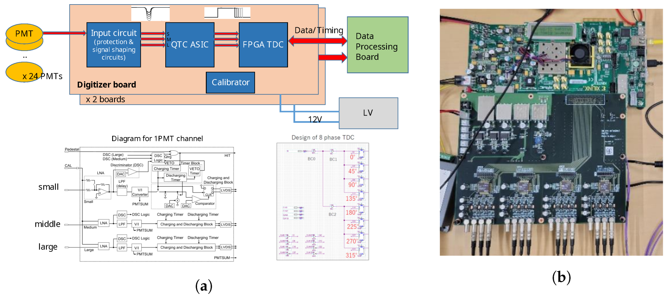
This design consists of pipeline of charge-to-time converter (QTC) and time-to-digital converter (TDC).
Figure 1 shows a block diagram. A QTC converts a PMT pulse into a digital pulse so that the timing width is proportional to the charge. Then, a TDC converts the first edge of the QTC pulse as signal timing and the width as signal charge simultaneously.
This scheme is implemented as custom QTC-ASIC for current SK electronics [
6] and has worked well for over ten years. For use in HK, we plan to reproduce the same custom QTC ASIC, with the same mask, fabrication lane, and so on, to assure there is no degradation in performance, especially in failure rate and reliability. In addition, we have developed high-speed TDC on FPGA since the TDC used in SK has been discontinued. It achieves
timing resolution [
7].
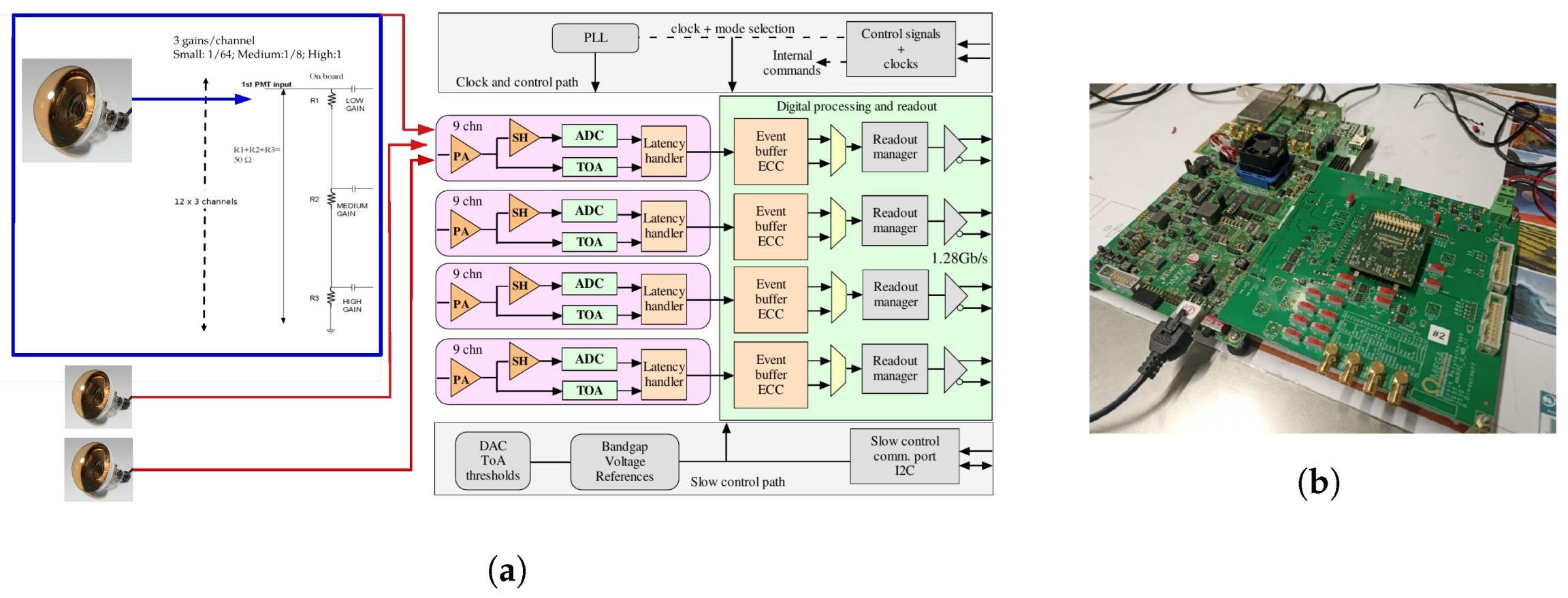
3.2. Custom FADC-ASIC Design (HKROC)
The basic principle is digitizing the PMT signal as a waveform and then calculating integrated charge and timing.
Figure 2 shows a basic block diagram. FADC and signal processors are implemented as a custom ASIC called “HKROC”. The HKROC can digitize signal waveform continuously, like an oscilloscope. Typical FADCs have too much power consumption to meet our requirements. The HKROC is well designed to have low power consumption. In practice, we plan to operate it so that HKROC saves several sampling points per pulse-like event to suppress data size. Thanks to the FADC scheme, it has a short dead time, which has a significant impact on physics.
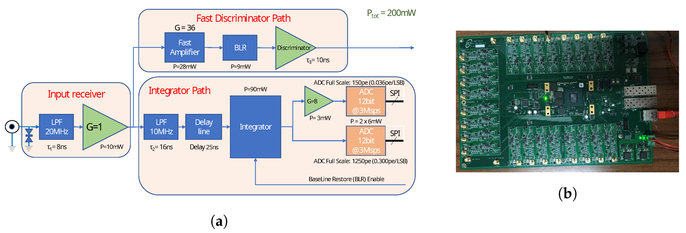
3.3. Discrete Design
This design consists of an integrator path, whose output is sampled by two ADCs, for charge measurement, and a fast discriminator for TDC timing measurement, as shown in
Figure 3. The name “discrete design” comes from the implementation method which uses discrete components such as commercial ADC chips, a comparator, and so on. It provides higher tunability and easier revision and helps with faster development. The separation of charge and timing paths allows additional information to be gathered from the Time over Threshold (ToT) measure, which is complementary information of charge measured by the ADC and allows detection of the pre or late pulses of the PMT.
3.4. Performance Evaluation
We have measured or estimated all requirements with the prototypes explained in each subsection. All results met our basic requirements in the systematic test. The basic performances are measured as the same levels we set as requirements.
Table 3 shows some of the results of basic performance. In addition, HKROC has a fast response. In case of the same input charge level, it achieves signal distinguishment displaced by
.
Basic performances were kept in the test with the actual PMTs. During the measurement of the discrete design, we confirmed low ToT signals even if the main charge taken by the ADC showed a nominal level. This indicates pre or late pulses of the PMTs.
4. Discussion
We have selected the discrete design as our digitizer for HK. The decision was not only based on performance evaluation. Since the discrete design has good enough performance of basic requirements, an additional feature of ToT, and less risk in its schedule, we decided on this design. As I showed, all designs show excellent performance as a PMT readout system and fulfill the stringent requirement of one of the future world-leading experiments. They are usable for other applications out of HK.
The next phase of our digitizer development is finalizing the design for mass production. We are integrating components as whole front-end electronics, such as low-voltage power supply and a data handling board, and planning to conduct long-term system tests underwater. In addition, we are considering utilizing the digitizer not only for the PMT but also for PMTs of outer muon veto detector.
5. Conclusions
In this paper, I have summarized digitizer options for Hyper-Kamiokande using large aperture PMTs of diameter as the main detector component. We have developed a prototype according to three different technologies: the custom QTC-ASIC, and TDC design, the custom FADC-ASIC design (HKROC), and the discrete design. Those performances fulfill the requirements defined by characteristics of the Water Cherenkov detector, observing from a few up to events. After a detailed review and discussion, HK collaboration has selected the discrete design for our digitizer. We are now finalizing the design for mass production and planning to conduct long-term system tests underwater.
Funding
The author is supported by JST, the establishment of university fellowships towards the creation of science technology innovation, Grant Number JPMJFS2112.
Institutional Review Board Statement
Not applicable.
Informed Consent Statement
Not applicable.
Data Availability Statement
Not applicable.
Conflicts of Interest
The author declares no conflict of interest. The funders had no role in the design of the study; in the collection, analyses, or interpretation of data; in the writing of the manuscript; or in the decision to publish the results.
References
- Abe, K.; Abe, K.; Aihara, H.; Aimi, A.; Akutsu, R.; Andreopoulos, C.; Anghel, I.; Anthony, L.H.V.; Antonova, M.; Ashida, Y.; et al. Hyper-Kamiokande Design Report. arXiv 2018, arXiv:1805.04163. [Google Scholar]
- Yamazaki, Y.; Hasegawa, K.; Ikegami, M.; Irie, Y.; Kato, T.; Kobayashi, H.; Machida, S.; Mori, Y.; Noda, F.; Suzuki, H.; et al. Accelerator technical design report for J-PARC. KEK Rep. 2002, 13, 2003-044. [Google Scholar]
- Itow, Y. Construction status and prospects of the Hyper-Kamiokande project. In Proceedings of the 37th International Cosmic Ray Conference (ICRC2021), Berlin, Germany, 12–23 July 2021; p. 1192. [Google Scholar] [CrossRef]
- Fukuda, Y.; Fukuda, Y.; Hayakawa, T.; Ichihara, E.; Ishitsuka, M.; Itow, Y.; Kajita, T.; Kameda, J.; Kaneyuki, K.; Kasuga, S.; et al. The Super-Kamiokande detector. Nucl. Instrum. Methods A 2003, 501, 418–462. [Google Scholar] [CrossRef]
- Tashiro, T. Preparation of large aperture Photo-Detectors for the Hyper-Kamiokande. In Proceedings of the 40th International Conference on High Energy physics (ICHEP2020), Prague, Czech Republic, 28 July–6 August 2021; p. 876. [Google Scholar] [CrossRef]
- Nishino, H.; Awai, K.; Hayato, Y.; Nakayama, S.; Okumura, K.; Shiozawa, M.; Takeda, A.; Ishikawa, K.; Minegishi, A.; Arai, Y. High-speed charge-to-time converter ASIC for the Super-Kamiokande detector. Nucl. Instrum. Methods A 2009, 610, 710–717. [Google Scholar] [CrossRef] [Green Version]
- Kataoka, Y.; Hayato, Y. Signal Digitizer based on FPGA TDC for Hyper-Kamiokande experiment. In Proceedings of the 2018 IEEE Nuclear Science Symposium and Medical Imaging Conference, Sydney, Australia, 10–17 November 2018. [Google Scholar] [CrossRef]
| Disclaimer/Publisher’s Note: The statements, opinions and data contained in all publications are solely those of the individual author(s) and contributor(s) and not of MDPI and/or the editor(s). MDPI and/or the editor(s) disclaim responsibility for any injury to people or property resulting from any ideas, methods, instructions or products referred to in the content. |
© 2023 by the author. Licensee MDPI, Basel, Switzerland. This article is an open access article distributed under the terms and conditions of the Creative Commons Attribution (CC BY) license (https://creativecommons.org/licenses/by/4.0/).


