

Reverse-Bias Defect Creation in Cu(In,Ga)Se2 Solar Cells and Impact of Encapsulation

Abstract
:1. Introduction
2. Experimental
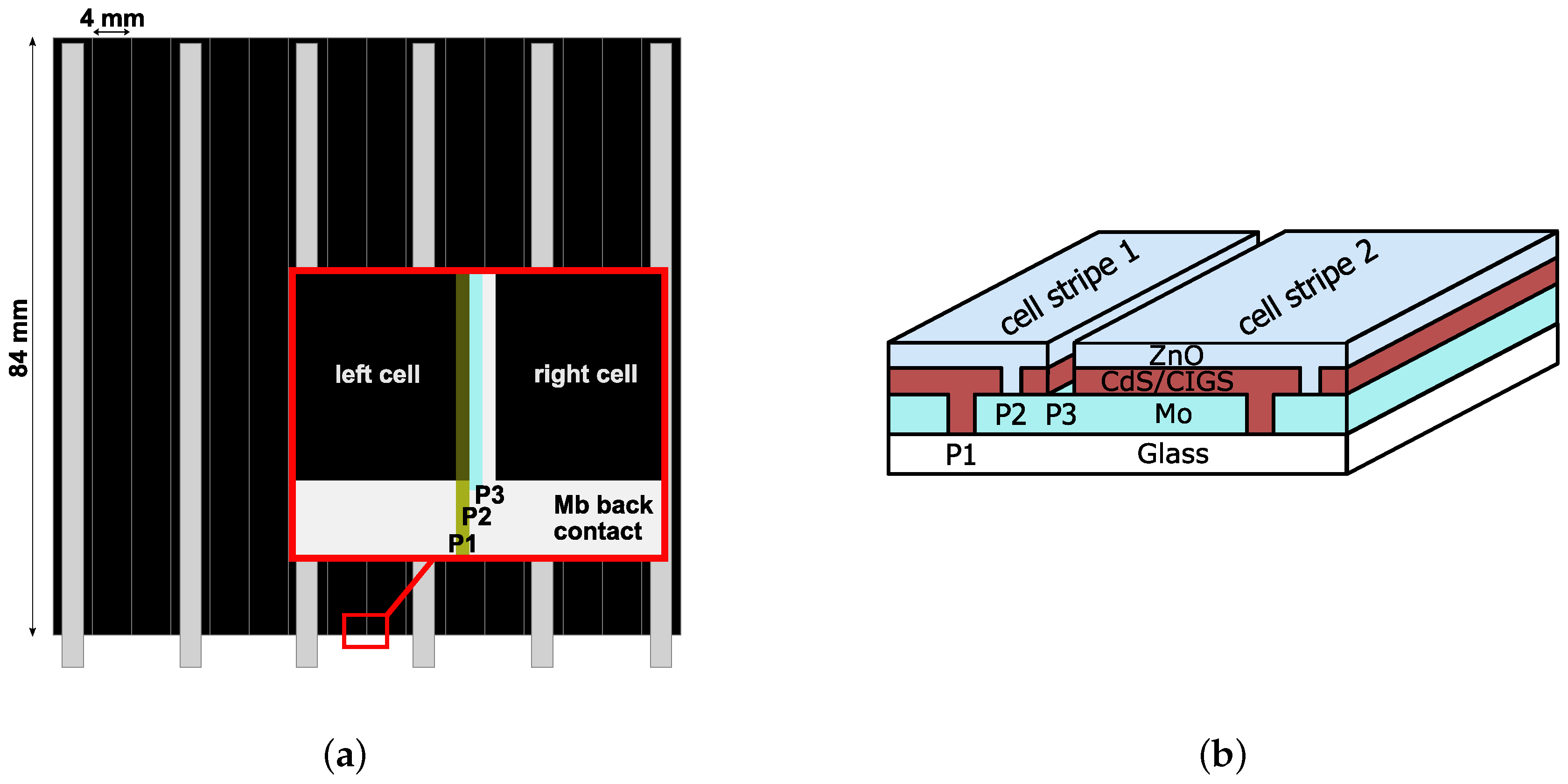
2.1. Samples and Set-Up
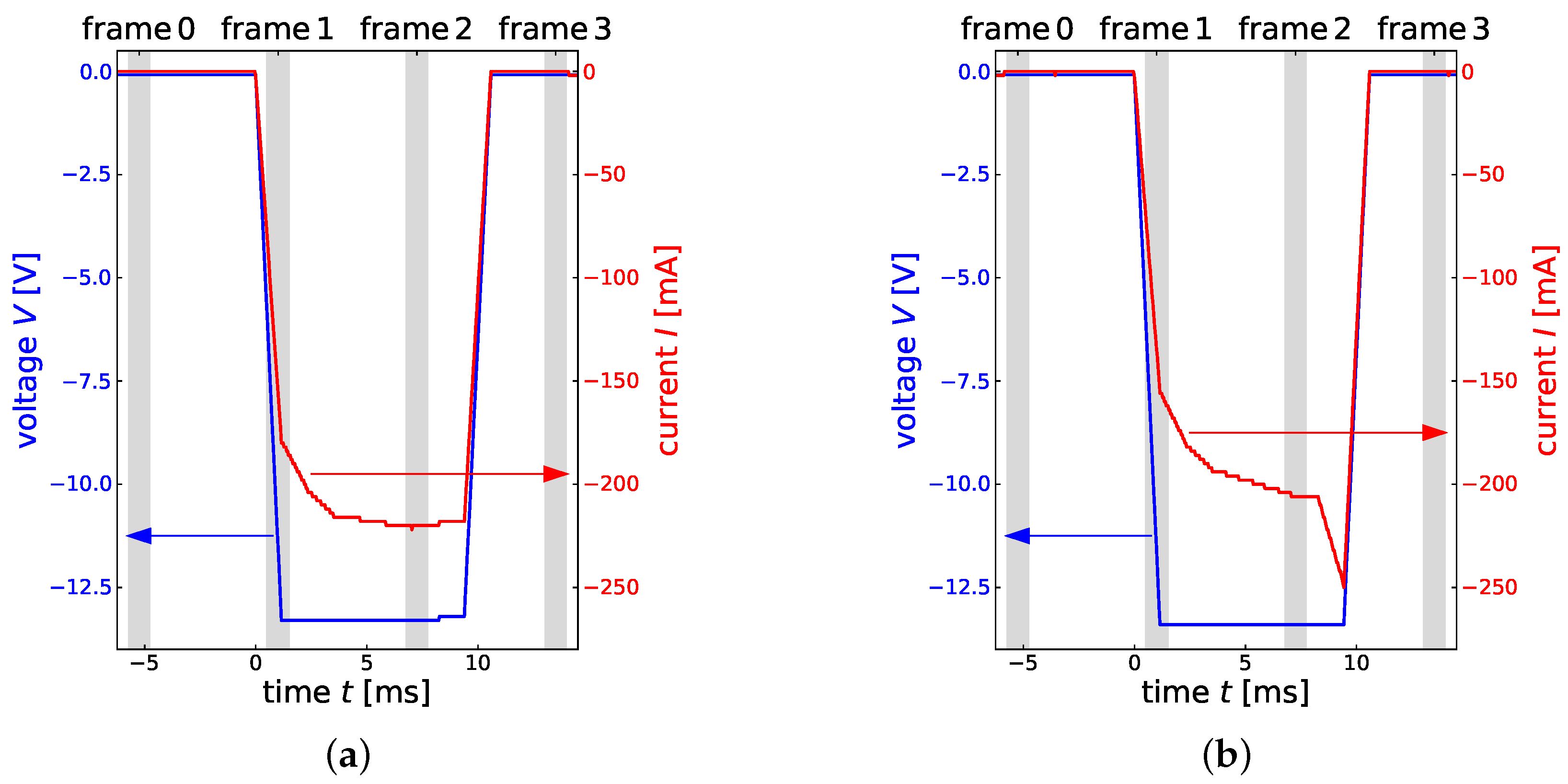
2.2. Experiment
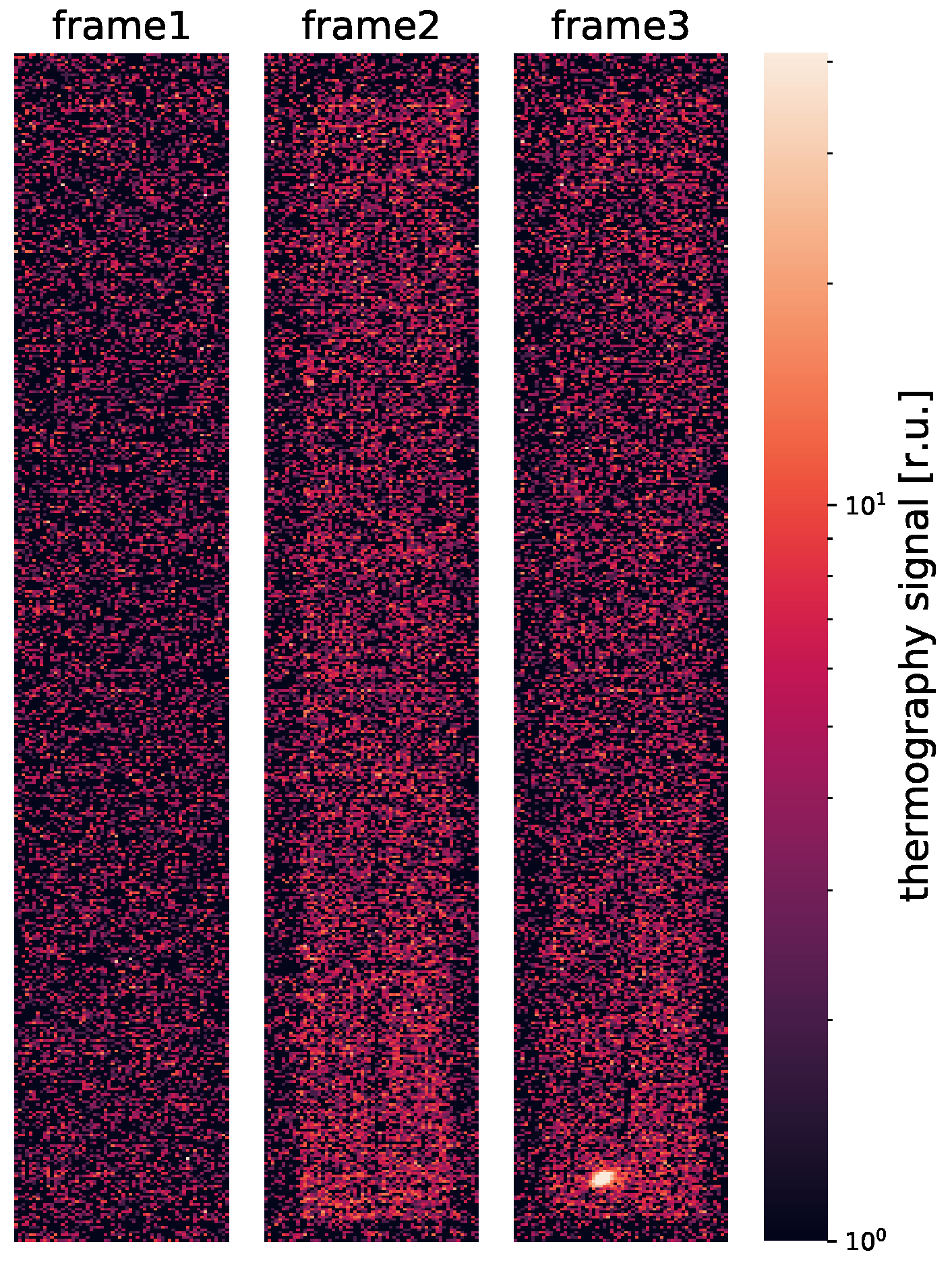
3. Results
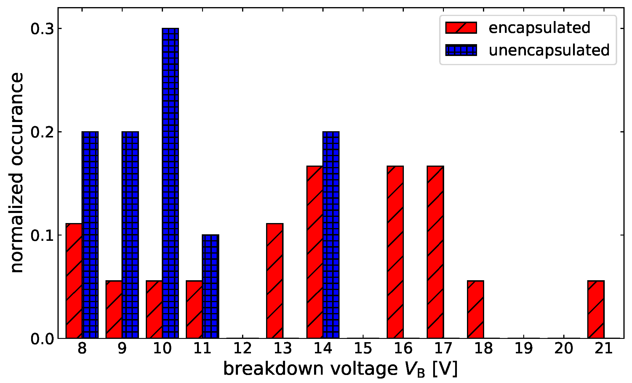
3.1. Reverse Breakdown Behavior
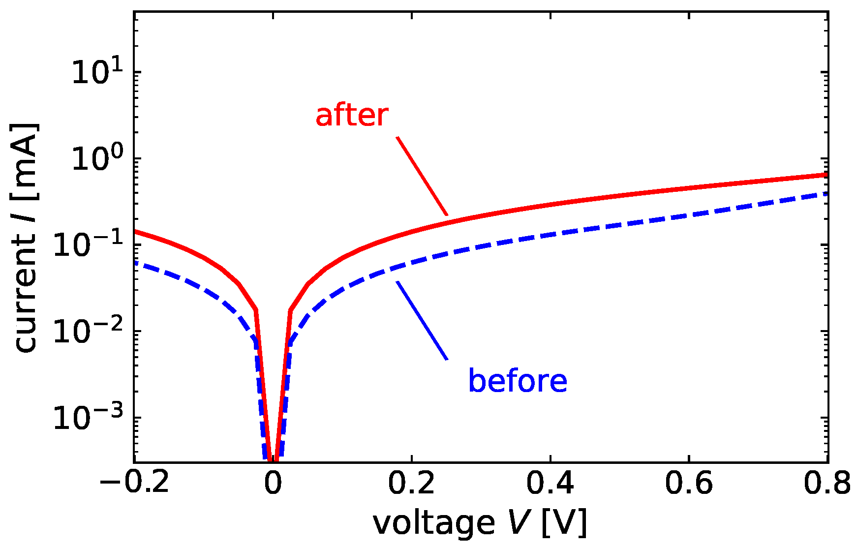
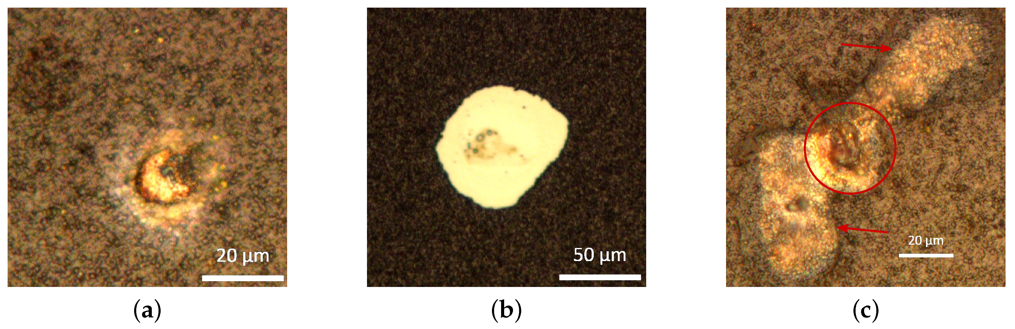
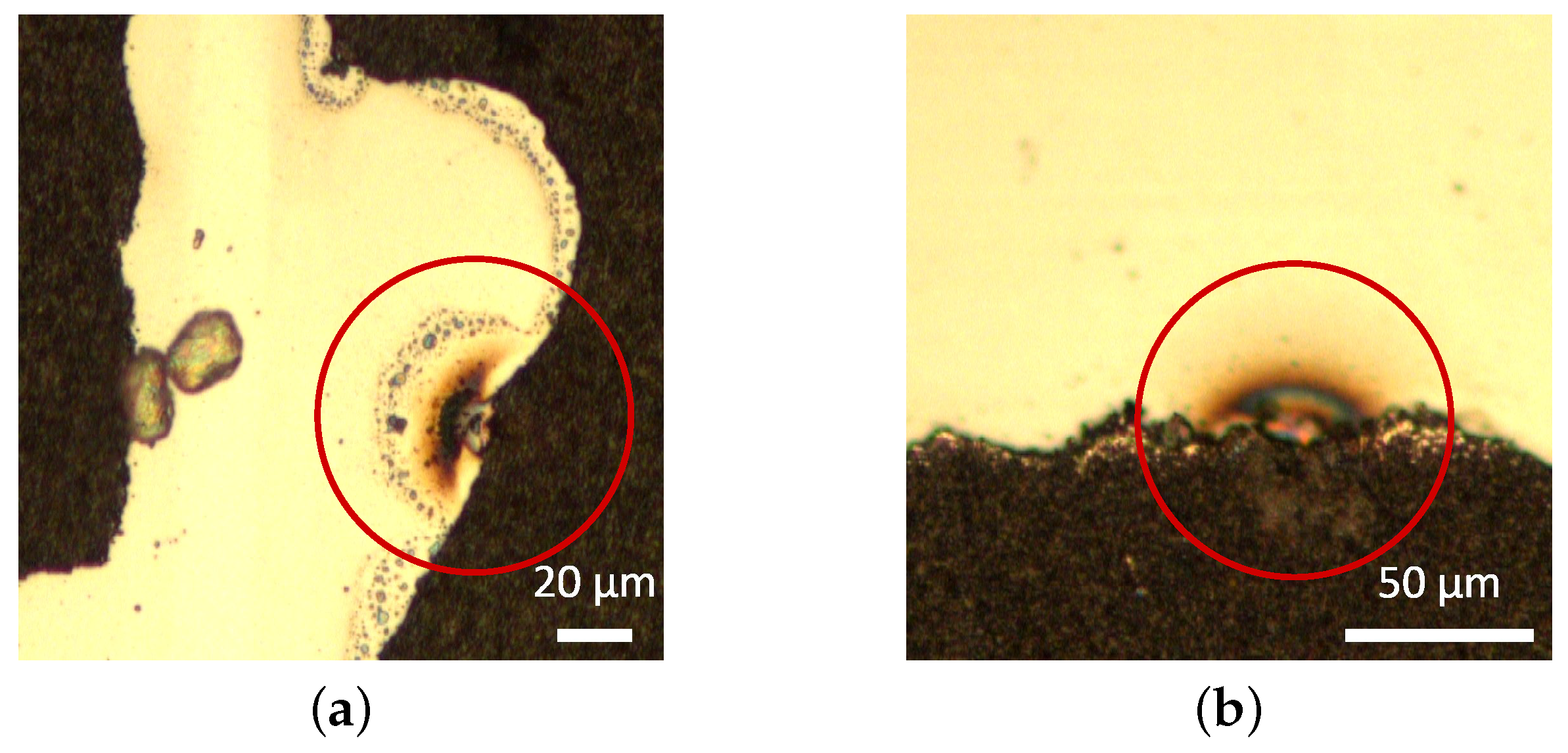
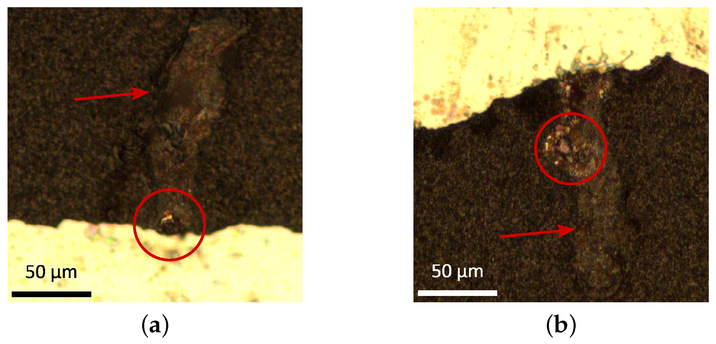
3.2. Post Mortem Analysis
- Defects within the solar cell area;
- Defects at the edge/P3;
- Defects at the P1 line.
4. Discussion
5. Summary
Author Contributions
Funding
Conflicts of Interest
References
- Molenbroek, E.; Waddington, D.; Emery, K. Hot spot susceptibility and testing of PV modules. In Proceedings of the IEEE 22nd Photovoltaic Specialists Conference, Las Vegas, NV, USA, 7–11 October 1991; pp. 547–552. [Google Scholar]
- Johnston, S.; Sulas, D.; Palmiotti, E.; Gerber, A.; Guthrey, H.; Liu, J.; Mansfield, L.; Silverman, T.J.; Rockett, A.; Al-Jassim, M. Thin-film module reverse-bias breakdown sites identified by thermal imaging. In Proceedings of the IEEE 7th World Conference on Photovoltaic Energy Conversion (A Joint Conference of 45th IEEE PVSC, 28th PVSEC & 34th EU PVSEC), Waikoloa Village, HI, USA, 10–15 June 2018; pp. 1897–1901. [Google Scholar]
- Bakker, K.; Weeber, A.; Theelen, M. Reliability implications of partial shading on CIGS photovoltaic devices: A literature review. J. Mater. Res. 2019, 34, 3977–3987. [Google Scholar] [CrossRef]
- Silverman, T.J.; Deceglie, M.G.; Deline, C.; Kurtz, S. Partial shade stress test for thin-film photovoltaic modules. In Proceedings of the SPIE Reliability of Photovoltaic Cells, Modules, Components, and Systems VIII, San Diego, CA, USA, 9–10 August 2015; pp. 112–123. [Google Scholar]
- Wendlandt, S.; Berendes, S.; Weber, T.; Berghold, J.; Krauter, S.; Grunow, P. Shadowing investigations on thin film modules. In Proceedings of the 32nd European Photovoltaic Solar Energy Conference and Exhibition, Munich, Germany, 20–24 June 2016. [Google Scholar]
- Silverman, T.J.; Mansfield, L.; Repins, I.; Kurtz, S. Damage in monolithic thin-film photovoltaic modules due to partial shade. IEEE J. Photovolt. 2016, 6, 1333–1338. [Google Scholar] [CrossRef]
- Lee, J.E.; Bae, S.; Oh, W.; Park, H.; Kim, S.M.; Lee, D.; Nam, J.; Mo, C.B.; Kim, D.; Yang, J.; et al. Investigation of damage caused by partial shading of CuInxGa(1-x)Se2 photovoltaic modules with bypass diodes. Prog. Photovolt. Res. Appl. 2016, 24, 1035–1043. [Google Scholar] [CrossRef]
- Wendlandt, S.; Podlowski, L. Influence of near field shadowing on the performance ratio of thin film modules. In Proceedings of the 35th European Photovoltaic Solar Energy Conference and Exhibition, Brussel, Belgium, 24–27 September 2018; pp. 1230–1235. [Google Scholar]
- Westin, P.O.; Zimmermann, U.; Stolt, L.; Edoff, M. Reverse bias damage in CIGS modules. In Proceedings of the 24th European Photovoltaic Solar Energy Conference, Hamburg, Germany, 21–25 September 2009; pp. 2967–2970. [Google Scholar]
- Johnston, S.; Palmiotti, E.; Gerber, A.; Guthrey, H.; Mansfield, L.; Silverman, T.J.; Al-Jassim, M.; Rockett, A. Identifying reverse-bias breakdown sites in CuInxGa(1-x)Se2. In Proceedings of the IEEE 44th Photovoltaic Specialist Conference, Washington, DC, USA, 25–30 June 2017; pp. 1400–1404. [Google Scholar]
- Palmiotti, E.; Johnston, S.; Gerber, A.; Guthrey, H.; Rockett, A.; Mansfield, L.; Silverman, T.J.; Al-Jassim, M. Identification and analysis of partial shading breakdown sites in CuInxGa(1-x)Se2 modules. Sol. Energy 2018, 161, 1–5. [Google Scholar] [CrossRef]
- Guthrey, H.; Nardone, M.; Johnston, S.; Liu, J.; Norman, A.; Moseley, J.; Al-Jassim, M. Characterization and modeling of reverse-bias breakdown in Cu(In,Ga)Se2 photovoltaic devices. Prog. Photovolt. Res. Appl. 2019, 27, 812–823. [Google Scholar] [CrossRef]
- Bakker, K.; Åhman, H.N.; Burgers, T.; Barreau, N.; Weeber, A.; Theelen, M. Propagation mechanism of reverse bias induced defects in Cu(In,Ga)Se2 solar cells. Sol. Energy Mater. Sol. Cells 2020, 205, 110249. [Google Scholar] [CrossRef]
- Szaniawski, P.; Lindahl, J.; Törndahl, T.; Zimmermann, U.; Edoff, M. Light-enhanced reverse breakdown in Cu(In,Ga)Se2 solar cells. Thin Solid Film. 2013, 535, 326–330. [Google Scholar] [CrossRef]
- Puttnins, S.; Jander, S.; Wehrmann, A.; Benndorf, G.; Stölzel, M.; Müller, A.; Von Wenckstern, H.; Daume, F.; Rahm, A.; Grundmann, M. Breakdown characteristics of flexible Cu(In,Ga)Se2 solar cells. Sol. Energy Mater. Sol. Cells 2014, 120, 506–511. [Google Scholar] [CrossRef]
- Dimmler, B.; Wächter, R. Manufacturing and application of CIS solar modules. Thin Solid Film. 2007, 515, 5973–5978. [Google Scholar] [CrossRef]
- IRCAM Works, Version 3.02. Windows. IRCAM GmbH: Bayern, Germany, 2007.
- Babrauskas, V. Arc breakdown in air over very small gap distances. In Proceedings of the 13th International Fire Science and Engineering Conference, Nr Windsor, UK, 24–26 June 2013; Volume 2, pp. 1489–1498. [Google Scholar]
- Karpov, V. Coupled electron–heat transport in nonuniform thin film semiconductor structures. Phys. Rev. B 2012, 86, 165317. [Google Scholar] [CrossRef] [Green Version]
- Nardone, M.; Dahal, S.; Waddle, J. Shading-induced failure in thin-film photovoltaic modules: Electrothermal simulation with nonuniformities. Sol. Energy 2016, 139, 381–388. [Google Scholar] [CrossRef] [Green Version]
- Vaas, T.S.; Pieters, B.E.; Gerber, A.; Rau, U. Thermal Stimulation of Reverse Breakdown in CIGS Solar Cells. IEEE J. Photovolt. 2023. [Google Scholar] [CrossRef]
- Nofal, S.; Pieters, B.E.; Hülsbeck, M.; Zahren, C.; Gerber, A.; Rau, U. A direct measure of positive feedback loop-gain due to reverse bias damage in thin-film solar cells using lock-in thermography. EPJ Photovolt. 2023, 14, 3. [Google Scholar] [CrossRef]
- Williams, P.; Peterkin, F. A mechanism for surface flashover of semiconductors. In Proceedings of the 7th Pulsed Power Conference, Monterey, CA, USA, 11–14 June 1989; pp. 890–892. [Google Scholar] [CrossRef]


| Defect Location | Total | within | edge/P3 (Thereof Elongated) | P1 |
|---|---|---|---|---|
| encapsulated | 27 | 23 | 4 (4) | 0 |
| unencapsulated | 13 | 2 | 9 (1) | 2 |
Disclaimer/Publisher’s Note: The statements, opinions and data contained in all publications are solely those of the individual author(s) and contributor(s) and not of MDPI and/or the editor(s). MDPI and/or the editor(s) disclaim responsibility for any injury to people or property resulting from any ideas, methods, instructions or products referred to in the content. |
© 2023 by the authors. Licensee MDPI, Basel, Switzerland. This article is an open access article distributed under the terms and conditions of the Creative Commons Attribution (CC BY) license (https://creativecommons.org/licenses/by/4.0/).
Share and Cite
Vaas, T.S.; Pieters, B.E.; Gerber, A.; Rau, U. Reverse-Bias Defect Creation in Cu(In,Ga)Se2 Solar Cells and Impact of Encapsulation. Solar 2023, 3, 184-194. https://doi.org/10.3390/solar3020012
Vaas TS, Pieters BE, Gerber A, Rau U. Reverse-Bias Defect Creation in Cu(In,Ga)Se2 Solar Cells and Impact of Encapsulation. Solar. 2023; 3(2):184-194. https://doi.org/10.3390/solar3020012
Chicago/Turabian StyleVaas, Timon Sebastian, Bart Elger Pieters, Andreas Gerber, and Uwe Rau. 2023. "Reverse-Bias Defect Creation in Cu(In,Ga)Se2 Solar Cells and Impact of Encapsulation" Solar 3, no. 2: 184-194. https://doi.org/10.3390/solar3020012