Article

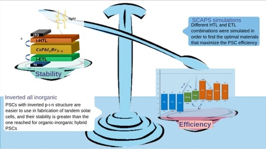
Optimization of Inverted All-Inorganic CsPbI3 and CsPbI2Br Perovskite Solar Cells by SCAPS-1D Simulation

by
Carlos Pinzón
1,
Nahuel Martínez
1,2,
Guillermo Casas
1,
Fernando C. Alvira
1,
Nicole Denon
3,
Gastón Brusasco
4,
Hugo Medina Chanduví
5,
Arles V. Gil Rebaza
4,5 and
Marcelo A. Cappelletti
3,6,*
1
Laboratorio de Simulación Control Biofotónica y Nanotecnología (SiCoBioNa), Science and Technology Department, Universidad Nacional de Quilmes, Roque Saenz Peña N° 352, Bernal 1876, Argentina
2
CIFICEN (UNCPBA-CICPBA-CONICET), Pinto N° 399, Tandil 7000, Argentina
3
Programa TICAPPS, Universidad Nacional Arturo Jauretche, Av. Calchaquí N° 6200, Florencio Varela 1888, Argentina
4
Departamento de Física, Facultad de Ciencias Exactas, Universidad Nacional de La Plata (UNLP), La Plata 1900, Argentina
5
Instituto de Física La Plata (IFLP), CCT La Plata—CONICET, La Plata 1900, Argentina
6
Grupo de Control Aplicado (GCA), Instituto LEICI (UNLP-CONICET), Facultad de Ingeniería, Universidad Nacional de La Plata, La Plata 1900, Argentina
*
Author to whom correspondence should be addressed.
Solar 2022, 2(4), 559-571; https://doi.org/10.3390/solar2040033
Submission received: 16 September 2022 / Revised: 24 November 2022 / Accepted: 28 November 2022 / Published: 9 December 2022

Abstract

:
Perovskite solar cells (PSCs) have substantially increased their power conversion efficiency (PCE) to more than 25% in recent years. However, the instability of these devices is still a strong obstacle for their commercial applications. Recently, all-inorganic PSCs based on CsPbI3 and CsPbI2Br as the perovskite layer have shown enhanced long-term stability, which makes them potential candidates for commercialization. Currently, all-inorganic PSCs with inverted p-i-n configuration have not yet reached the high efficiency achieved in the normal n-i-p structure. However, the inverted p-i-n architecture has recently drawn attention of researchers because it is more suitable to prepare tandem solar cells. In this work, a theoretical study of inverted p-i-n all-inorganic PSCs based on CsPbI3 and CsPbI2Br as the perovskite layer was carried out using SCAPS-1D software (ver. 3.3.09). The performance of different architectures of PSC was examined and compared by means of numerical simulations using various inorganic materials as the hole transport layer (HTL) and the electron transport layer (ETL). The results reveal that CuI and ZnO are the most suitable as HTL and ETL, respectively. In addition, the performance of the devices was significantly improved by optimizing the hole mobility in CuI as well as the thickness, doping density, and defect density in the absorber layer. Maximum efficiencies of 26.5% and 20.6% were obtained under optimized conditions for the inverted all-inorganic CsPbI3- and CsPbI2Br-based PSCs, respectively. These results indicate that further improvements in the performance of such devices are still possible.

Graphical Abstract

1. Introduction

The increase in energy consumption in recent years has promoted the use of new technologies based on renewable energy sources to generate electricity, with solar energy being one of the most promising alternatives. In this way, the study of solar cells, devices capable of converting light from the sun directly into electricity, is extremely important today. The study of microscopic properties of materials, in addition to advances in the manufacturing processes of the photovoltaic devices, has provided a path to develop new technologies in solar cells with higher performance and shorter processing time.
One of the developments that have gained special relevance in the last decade are perovskite solar cells (PSCs), which have emerged as a technology with the potential to revolutionize the photovoltaic industry. This is mainly due to their excellent optical and electronic properties such as tunable band gap, large absorption coefficient, high charge carrier mobility, long diffusion lengths, their simpler manufacturing process, and lower cost compared with conventional crystalline silicon solar cell [1,2,3].
The power conversion efficiencies (PCE) of PSCs have substantially increased from 3.8% in 2009 [4] to more than 25% today [5]. The highest efficiencies so far were obtained for the so-called organic–inorganic hybrid PSCs. These consist of a perovskite layer as a light-absorbing region sandwiched between a p-type hole transport layer (HTL) and an n-type electron transport layer (ETL). These devices have achieved efficiencies comparable to technologies already established in the market, such as thin film solar cells based on cadmium telluride (CdTe), copper indium gallium selenide (CIGS), or even, as silicon solar cells. These high-efficiency hybrid PSCs are based on methylammonium (CH3NH 3+ or MA) lead iodide (MAPbI3) and formamidinium (NH2CH=NH2+ or FA) lead iodide (FAPbI3) as light-harvesting materials. However, the long-term stability of organic–inorganic hybrid PSCs is still a serious problem because of their potential degradation under chemical and thermal pressure [6], which is a strong obstacle for their further development and commercial application [7,8]. In particular, MAPbI3 has proven to be unstable due to the high volatility of hydrophilic organic cations at high temperature (such as CH3NH3+). In comparison with MAPbI3, the FAPbI3 perovskite has shown superior thermal stability and even better photoelectric property [9], but phase stability has been a major cause of concern. FAPbI3 suffers a structural phase transition from black α-phase to non-perovskite yellow δ-phase at room temperature [10,11].
The replacement of volatile organic cations by inorganic components such as cesium (Cs+) has recently allowed the development of all-inorganic PSCs aiming to improve both the stability and efficiency of the devices [12,13,14,15,16,17]. All-inorganic CsPbIxBr3−x perovskite (with x between 0 and 3) have a band gap ranging from 1.73 eV (CsPbI3) to 2.31 eV (CsPbBr3) [18]. CsPbI3 has the most suitable band gap to fabricate high-efficiency PSCs, being therefore an ideal material to prepare tandem devices combined with either silicon or low band gap perovskite solar cells [19,20]. Although CsPbBr3 exhibits a great phase stability, the large band gap limits its efficiency [21]. For its part, CsPbI2Br perovskite possesses reasonable band gap (close to 1.9 eV) and phase stability, which makes it a great candidate for achieving a highly efficient and stable all-inorganic PSC, especially for the semitransparent and tandem solar cells [22,23].
Most of the high-performance all-inorganic PSCs reported so far are based on the normal n-i-p architecture due to their superiority in performance. CsPbI3 based PSCs in particular, have significantly enhanced the efficiency from 2.9% [24] to over 20% in 2022 [25,26]. On the other hand, a record power conversion efficiency of 17.51% was recently reported for the normal structure (n-i-p) CsPbI2Br cell [27].
Nowadays, there is increasing interest in the study of the all-inorganic PSCs with inverted p-i-n structure [28,29,30,31,32]. They offer some advantages compared with the conventional n-i-p architecture, such as lower hysteresis in current–voltage characteristics, and improved operability in the tandem solar cell fabrication process [28,29]. Inverted CsPbI3 and CsPbI2Br cells have recently reached efficiencies of up to 19.27% [33] and 14.62% [32], respectively. These values are still far from 25% for hybrid PSCs; therefore, further studies are needed to identify the factors that limit the performance of p–i–n PSCs. The performance of tandem solar cells can be improved by optimizing the design of the inverted all-inorganic PSCs separately. In this paper, a comparative theoretical analysis of inverted all-inorganic CsPbI3- and CsPbI2Br-based PSCs was conducted using modeling and simulation techniques. These are fundamental tools to predict and analyze the behavior of the photovoltaic cells. Four materials (NiO, Cu2O, CuSCN, and CuI) were proposed as the inorganic hole-transporting layer (i-HTL); and three materials (ZnO, TiO2, and SnO2) were used as the inorganic electron-transporting layer (i-ETL). These inorganic materials under consideration in this study are promising candidates for use in all-inorganic PSCs with inverted structure. The performance of the devices was evaluated for different thicknesses, acceptor densities, and defect densities in the perovskite layer to optimize the design of the structure and to enhance the efficiency of these inverted all-inorganic PSCs.

2. Simulation Details

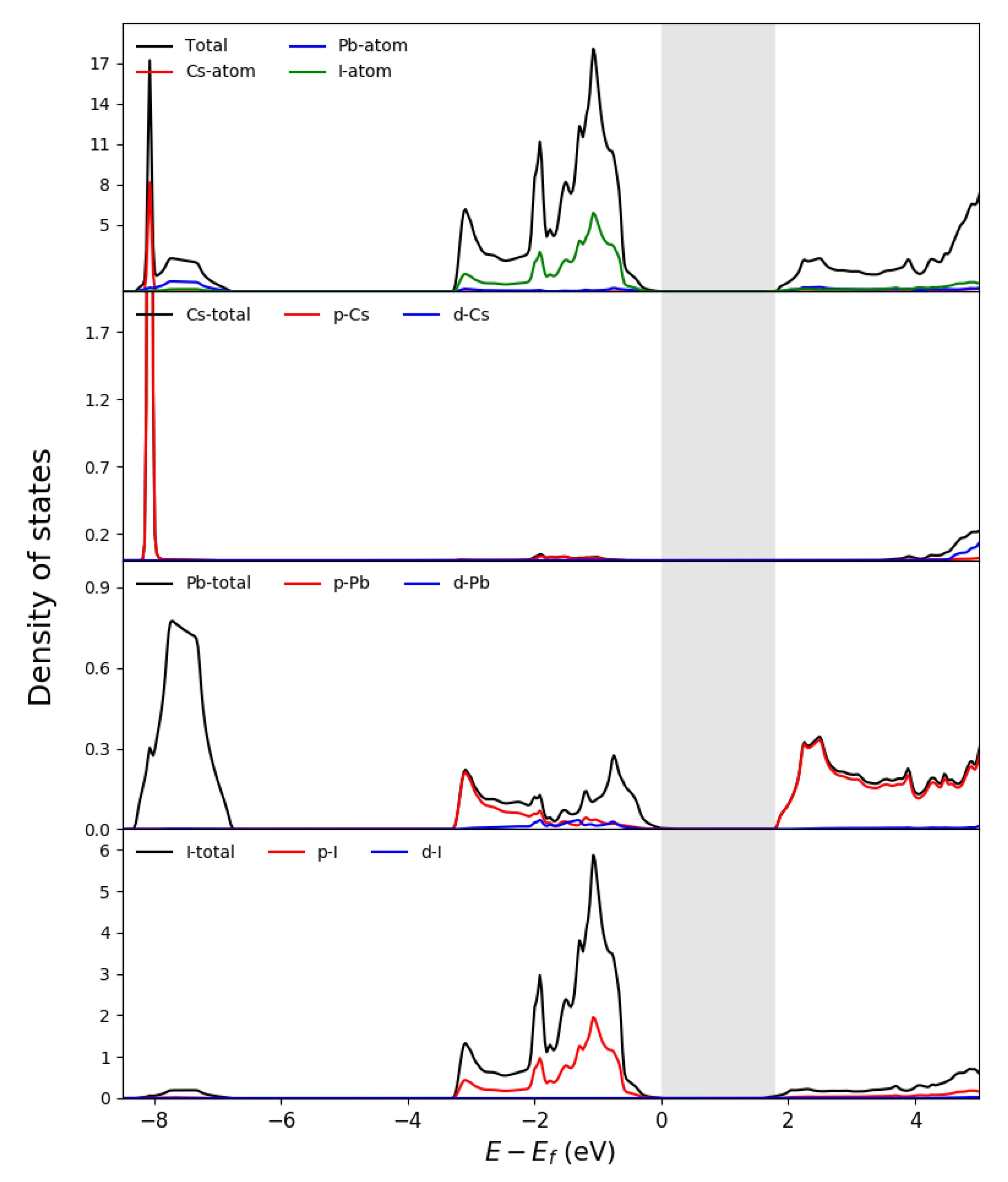
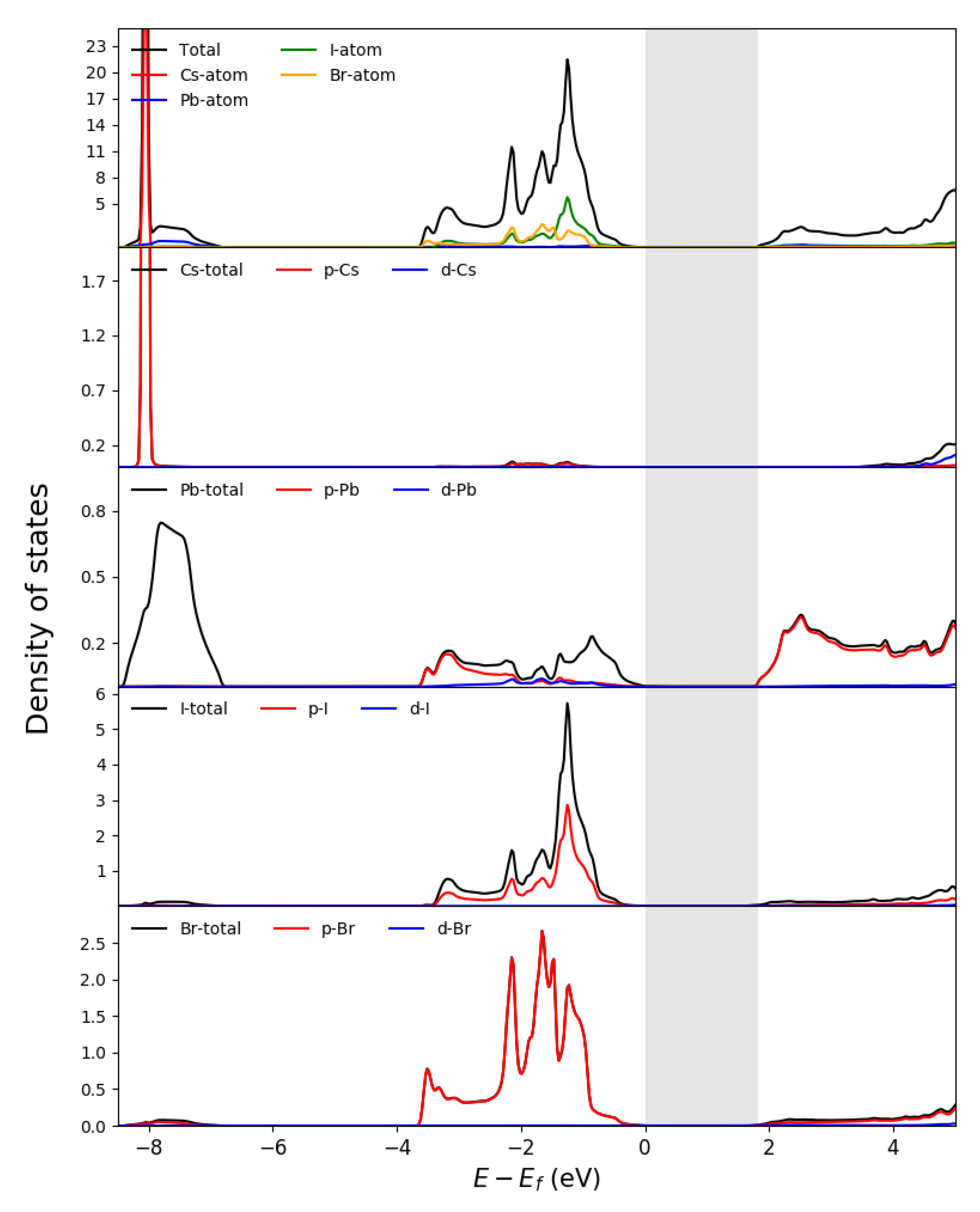
2.1. Electronic Structure Calculations

The electronic band structure of the cubic perovskite CsPbI3 with space group Pm-3m and CsPbI2Br with space group P4/mmm was studied from the first principles theory. These calculations are based on the Density Functional Theory (DFT) [34], and the self-consistent Kohn–Sham equation was solved using the Full-Potential Linearized Plane-Wave method (FP-LAPW) implemented in the Wien2k code [35,36]. The exchange-correlation (XC) functional was described using the Perdew–Burke–Ernzerhof (PBE) parametrization of the Generalized Gradient Approximation (GGA) [37]. In order to improve the electronic band structure of the compounds, the hybrid XC functional proposed by Heyd–Scuseria–Ernzerhof (HSE06) [38] was used. The muffin-tin radii employed was 2.0 bohr for the Cs, Pb, Br, and I atoms, whereas the parameter related with basic-set size was set to RMT × Kmax = 9 (RMT is the smallest muffin-tin radii and Kmax is related with the plane-wave cutoff). Regarding the reciprocal space, this was sampled using a dense mesh grid of 12 × 12 × 12 k points in the irreducible Brillouin zone.
The theoretical lattice parameters obtained were 6.398 Å and 6.0023 Å for the CsPbI3 and CsPbI2Br, respectively, which are in agreement with experimental values reported [39,40,41]. In order to obtain an accurate description of the electronic structures of the CsPbI3 and CsPbI2Br perovskites, we calculated the total and projected density of state (DOS) and the electronic band gap using the HSE06 hybrid functional, as seen in Figure 1 and Figure 2, respectively. Direct band gaps of 1.78 eV and 1.88 eV were found for the CsPbI3 and CsPbI2Br, respectively, in excellent agreement with the experimental values reported: 1.76 eV [42], 1.77 eV [43], and 1.79 eV [44] for the CsPbI3, and 1.82 eV [13], 1.86 eV [45], and 1.92 eV [46] for the CsPbI2Br. The band gap of the CsPbI3 perovskite is formed between the VBM, p-I orbital, and the CBM, p-Pb orbital. In the case of CsPbI2Br, the band gap is formed between the VBM, p-I, and p-Br orbitals, and the CBM, p-Pb orbital. For both compounds, the orbitals of the Cs atom are located far of the Fermi energy, as is shown in Figure 1 and Figure 2.

2.2. Device Simulations

Device simulations were performed with SCAPS-1D software [47], which is widely used and recognized by the scientific community related to PSCs [3,48,49,50,51,52,53]. This software numerically solves the system of the Poisson and the continuity equations for electrons and holes. The output parameters such as short-circuit current density (JSC), open circuit voltage (VOC), power conversion efficiency (PCE), maximum power point (PMAX), fill factor (FF), and external quantum efficiency (EQE) can be calculated using the SCAPS-1D software, in order to obtain the response of the device under different design and operating conditions.
Figure 3 shows the configuration of the all-inorganic PSC used in this work, which consists of an inverted structure ITO/i-HTL/CsPbIxBr3−x/i-ETL/Ag, for x equal to 2 and 3, where light enters through the i-HTL. The standard AM1.5G spectrum has been used.
Table 1, Table 2 and Table 3 summarize the main parameters used in the simulations for the perovskite layers, and for the materials chosen as i-HTL and i-ETL, respectively. Here NA and ND are the acceptor and donor density, respectively; εr is the relative permittivity; Ӽ is the electron affinity; EG is the band gap energy; μn and μp are the electron and hole mobilities, respectively; NT is the defect density; and NC and NV are the effective conduction and valence band density of states, respectively. The band gap energy and NC and NV values of Table 1 were obtained by means of DFT-based calculations. The rest of the values in Table 1, Table 2 and Table 3 are based on experimental and theoretical studies recently reported in the literature [51,54,55,56]. The absorption coefficient (α) was calculated from the Beer–Lambert law α = 2.303A/t [57], where A and t are the absorbance and thickness of film (350 nm), respectively. These were obtained from Wang 2020 [14] for the CsPbI3 layer and from Sutton 2016 [13] for the CsPbI2Br layer. The work functions of the front and back contacts are 4.7 eV (ITO) and 4.26 eV (Ag), respectively [58].
The energy level diagram of the i-ETL and i-HTL materials used in the simulation is shown in Figure 4. These levels play an important role in the performance of the device because they have a significant control on photocarrier transport. In order to facilitate proper electron transport, the conduction band minimum of the perovskite layer should be higher than that of the ETL. Similarly, the valence band maximum of the perovskite layer should be lower than that of the HTL for proper hole transport [59].

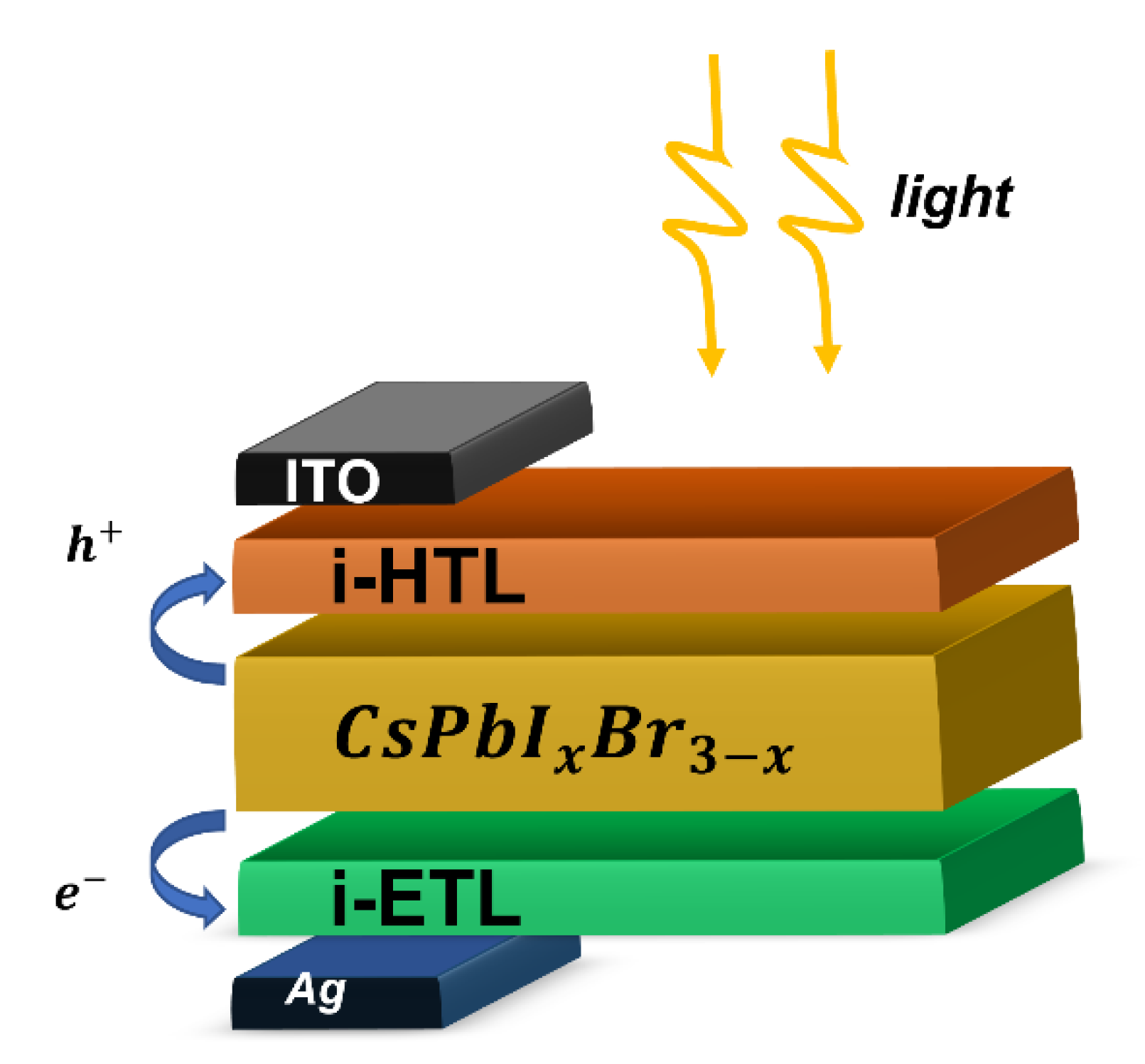
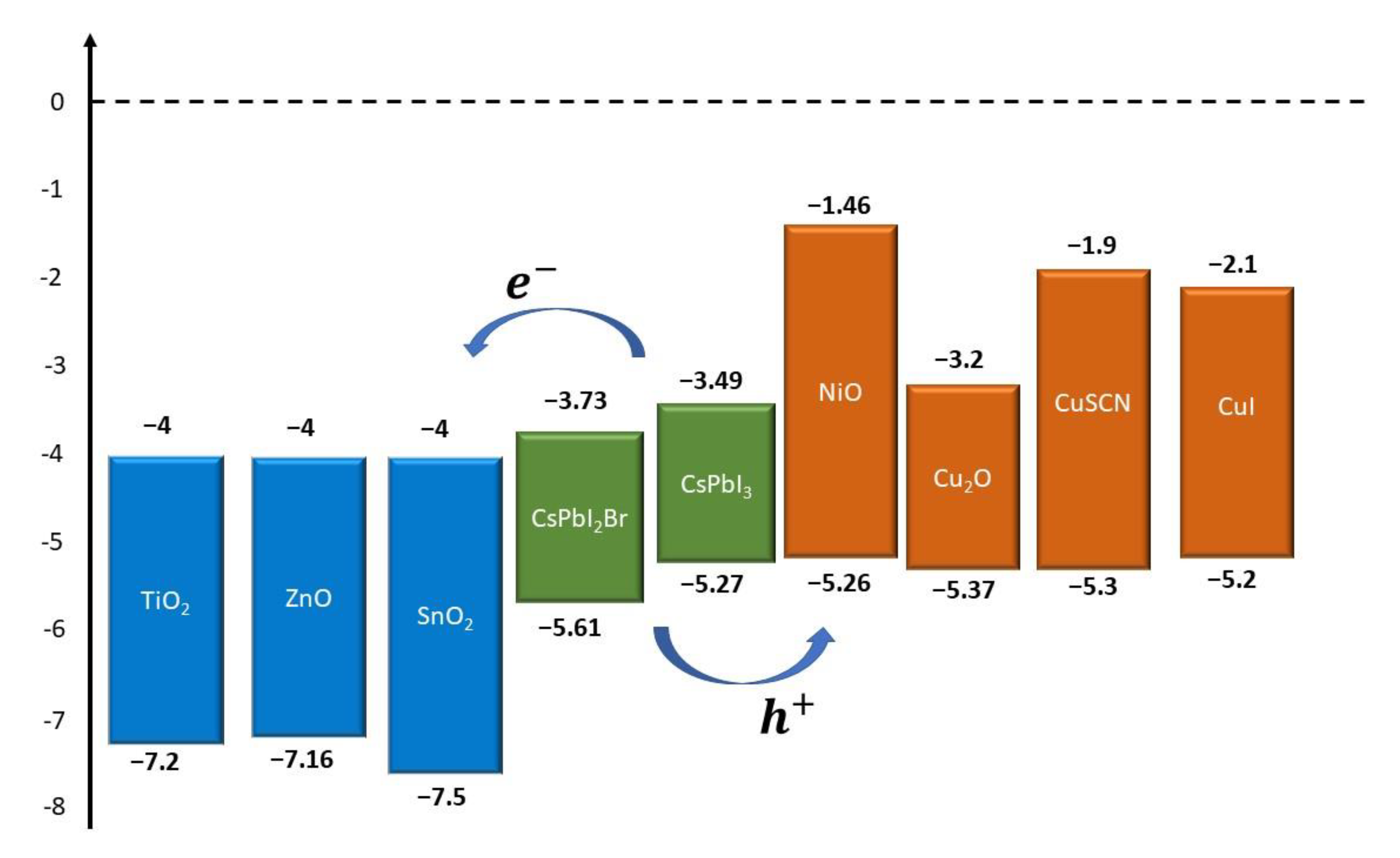
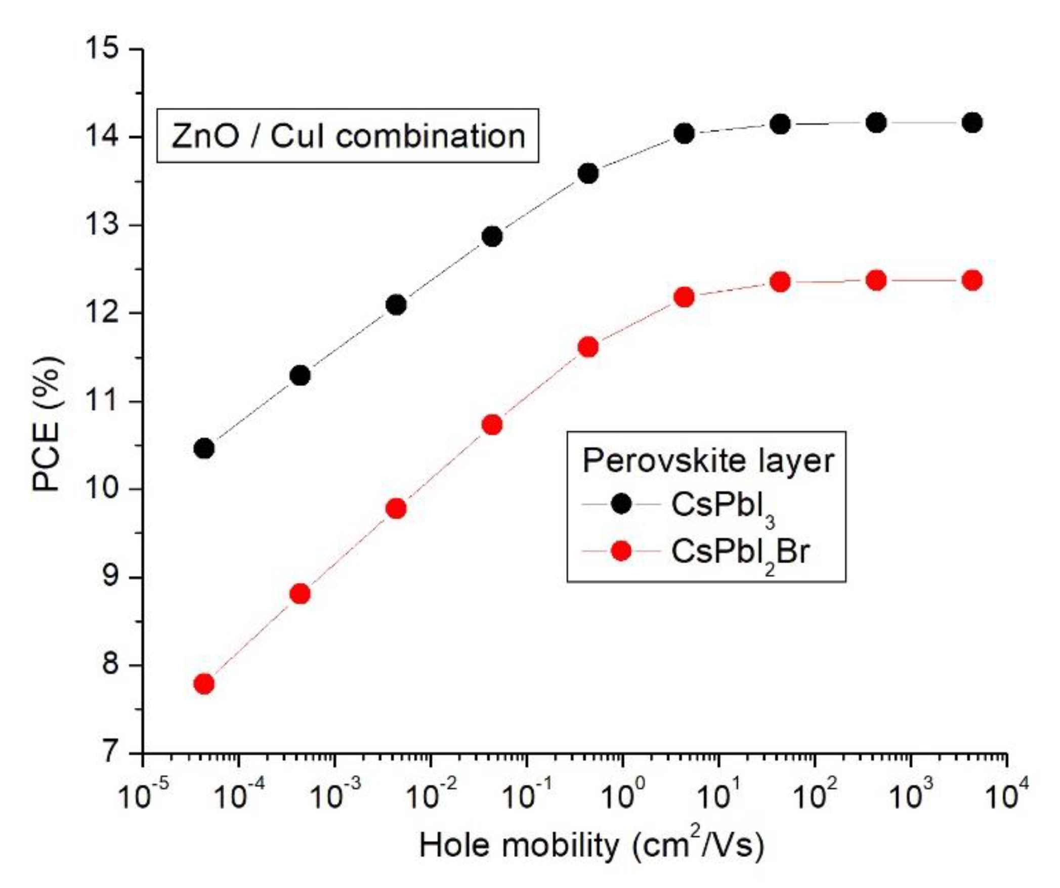
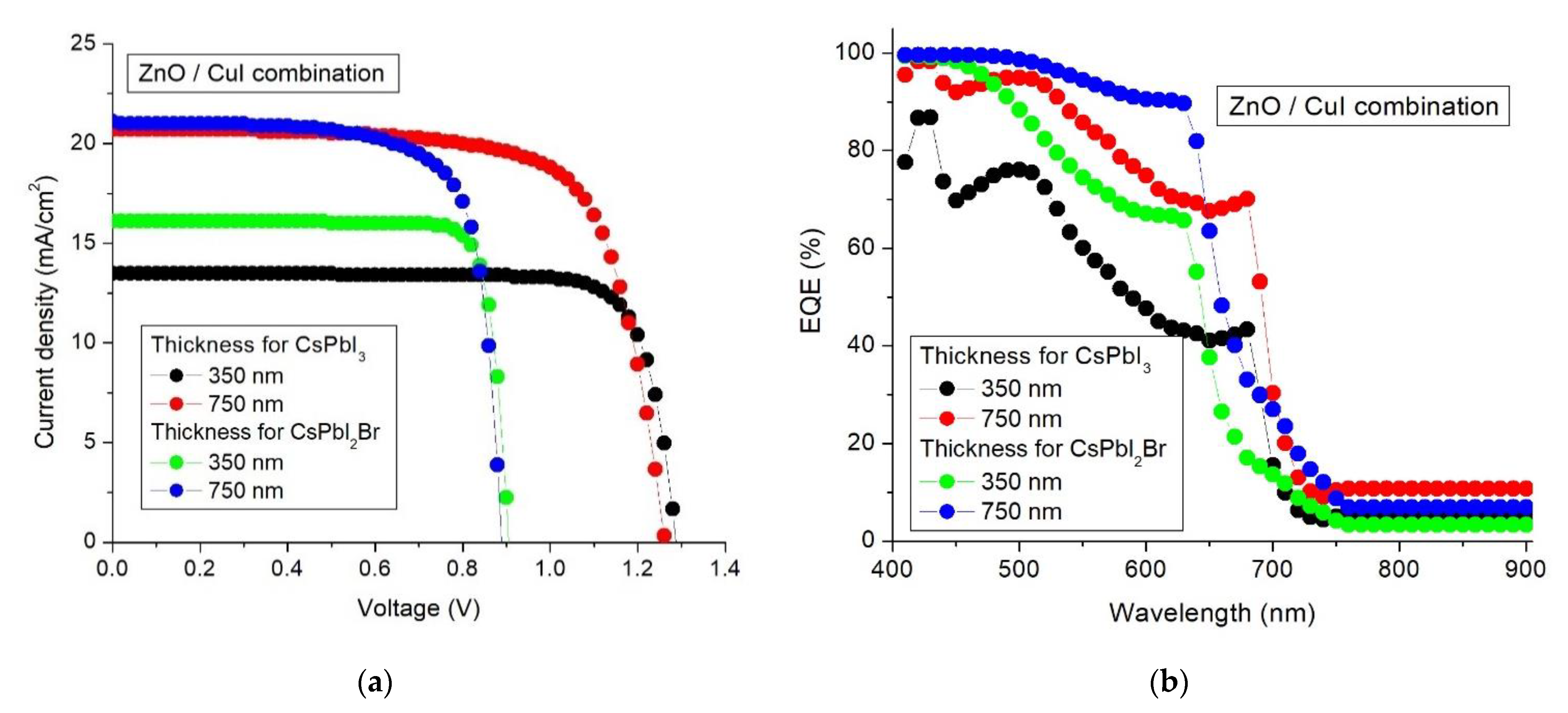
3. Results and Discussion

Using the values of Table 1, Table 2 and Table 3, an analysis of the twelve different possible combinations (i-ETL/i-HTL) of the inverted all-inorganic PSCs was carried out by means of SCAPS-1D software for each perovskite layer under study. The results of the output parameters (PCE, VOC, JSC, and FF) are summarized in Table 4. The first row in Table 4 corresponds to the materials used in [14]. The value of PCE of 14.03% obtained from simulations for the ZnO/NiO combination can be considered as a good approximation of the experimental result of 13.90% presented in Table 4 for the control device with the non-passivated perovskite film. It can also be observed in Table 4 that for the CsPbI3- and CsPbI2Br-based PSCs, the VOC values remain almost unchanged for all considered cases. On the other hand, PCE is the parameter with the greatest variations between their minimum and maximum values, approximately 24% and 14%, for the CsPbI3- and CsPbI2Br-based PSCs, respectively.
For ETL materials, the highest PCE values were obtained for ZnO, while the lowest PCE values were obtained for TiO2. TiO2 and ZnO have very similar properties (band structure, electronic affinity, relative permittivity, band gap energy, among others). However, TiO2 has higher NC and NV, and therefore higher intrinsic carrier concentration than ZnO. The larger the intrinsic carrier concentration, the higher the recombination rate and the smaller the carrier collection when the electric field is high (at voltages close to VOC). As a consequence of the aforementioned effects, lower FF and PCE were obtained for TiO2 compared with ZnO. Therefore, TiO2 is not the optimal material as ETL for CsPbI3 and CsPbI2Br perovskite solar cells as considered in this work.
On the other hand, the choice of HTL also influences the performance of the device. The band alignment of the HTL with the perovskite layer and the intrinsic carrier concentration of the HTL material are key factors as well as the band gap and the hole mobility. The energy level diagram shown in Figure 4 indicate that there are good band alignments between the valance band of perovskite and the four HTL materials considered in this work. However, Table 4 shows that for a given ETL, the lowest PCE values were obtained for Cu2O, while the highest PCE values were obtained for CuI. Although Cu2O and CuI have similar band alignment and hole mobility, Cu2O has higher NC and NV, and therefore a higher intrinsic carrier concentration and recombination rate than CuI. Cu2O also has the lowest band gap. Since light enters through the HTL in a direct (p–i–n) structure, some ultraviolet light does not reach the perovskite layer in Cu2O, resulting in the lowest JCC and PCE.
The highest PCE values of 14.13% (for CsPbI3) and 12.35% (for CsPbI2Br) were obtained for the ZnO/CuI combination. These materials have a suitable band alignment with the active layer. For this reason, ZnO and CuI can be considered as good options for i-ETL and i-HTL, respectively.
In the rest of this work, PSCs with the inverted structure of ITO/CuI/CsPbI3 (CsPbI2Br)/ZnO/Ag are studied in detail, using different hole mobilities in CuI and different thicknesses, acceptor densities, and defect densities for the perovskite layers.
Figure 5 shows the PCE as a function of hole mobility of CuI HTL for CsPbI3 and CsPbI2Br PSC. In both cases, PCE is gradually reduced as the hole mobility decreases below a critical value (around 40 cm2V−1s−1), which is directly related to a shorter carrier diffusion length. In a previous work, we have shown a similar result for the MAPbI3 PSCs [52]. When the carrier diffusion length is less than the thickness of the HTL material, most carriers recombine before reaching the contacts. PCE values of 10.5% (for CsPbI3) and 7.8% (for CsPbI2Br) were obtained for the lowest value of hole mobility considered (4 × 10⁻⁵ cm2V−1s−1). On the other hand, as hole mobility increases, the carrier diffusion length becomes much greater than the HTL thickness, thereby facilitating carrier transport without significant recombination. Figure 5 shows that the PCE saturates for hole mobility values greater than 40 cm2V−1s−1. Therefore, the hole mobility value of 44 cm2V−1s−1 used in the simulations is appropriate to obtain a better performance of the devices.
From here, the study was focused on the perovskite layer, in which light is absorbed to produce photo-generated carriers, thus playing a decisive role in the device performance.
Figure 6 shows the J-V characteristics (a) and EQE spectrum (b) for CsPbI3 and CsPbI2Br devices for two different thicknesses of the absorber film: 350 and 750 nm. We can see that a slight reduction in VOC but a significant increase in JSC were obtained when the absorber thickness increased from 350 to 750 nm. This behavior is consistent with the EQE results. Since it is possible to improve the device efficiency by increasing the absorber thickness, Figure 7 shows the variation in the electrical parameters (PCE, VOC, JSC, and FF) when the CsPbI3 and CsPbI2Br thickness is increased from 250 nm. The values displayed in this figure are normalized to those corresponding to the thickness of 350 nm, previously shown in Table 4 for ZnO as i-ETL and CuI as i-HTL.
We can see in Figure 7a that when the CsPbI3 thickness increases from 250 to 1750 nm, the VOC and FF decrease by 4% and 35%, respectively. The drop in VOC can be explained by the dependence of this parameter on the photogenerated current and the dark saturation current. An increase in the dark saturation current promotes carrier recombination, which leads to a drop in VOC with increasing thickness. Furthermore, the strong decrease in FF with increasing thickness of the active layer can be explained by the increase in series resistance. In contrast, the JSC is strongly increased above 80% with increasing CsPbI3 thickness. This remarkable increase is due to the enhanced light absorption and, consequently, a higher concentration of free carriers that can be generated by photons and collected by the electrode. In the case of the PCE parameter, a significant increase by 30% is seen when the thickness is increased from 250 to 750 nm and then it starts to decrease for thicker films.
Similarly, we can see in Figure 7b that when the CsPbI2Br thickness increases from 250 to 1050 nm, the VOC and FF parameters decrease by 4% and 36%, respectively, whereas JSC increases by 40%, as the increase in the CsPbI2Br thickness. Furthermore, the PCE value is improved by 15% for a CsPbI2Br thickness of 650 nm relative to the thickness of 350 nm. Extending the thickness beyond 650 nm increases the recombination current and series resistance and thus reduces the PCE. In the CsPbI2Br PSC, the maximum value of PCE is reached for a lower thickness compared with the CsPbI3 cell. This is due to the fact that the defect density in the CsPbI2Br layer is two orders of magnitude higher than in CsPbI3 (see Table 1), which reduces the carrier diffusion length. Therefore, values of 750 nm and 650 nm were considered as the optimized values of the CsPbI3 and CsPbI2Br absorber thickness, respectively.
On the other hand, Figure 8 shows the variation of the PCE as a function of the acceptor density in the CsPbI3 and CsPbI2Br perovskite layer, respectively. We can see in both cases that when the acceptor density increases from 1013 to 1015 cm−3, the PCE remains constant, while this parameter decreases for higher values of 1015 cm−3. Therefore, an optimal value of 1015 cm−3 was chosen for NA.
Finally, the simulation results show that when optimized parameters are used with the CsPbI3- and CsPbI2B-based PSCs with the fixed values of NT presented in Table 1, the PCE values increase from 14.13% to 18.9% and from 12.35% to 14.37%, respectively, such as is shown in Figure 9. Additionally, this figure shows that the defect density NT of the perovskite layer has a significant impact on device performance. This is because more defects in the active layer shorten the minority-carrier diffusion length, and hence the photogenerated carriers recombine before reaching their respective electrode and thus do not contribute to improving device performance. Figure 9 shows the performance improvement that could be achieved by reducing the defect density. Optimum efficiencies of 26.5% and 20.6% could be obtained at defect density of the order of 1012 cm−3 for the inverted device with a structure of ITO/CuI/CsPbI3/ZnO/Ag and ITO/CuI/CsPbI2Br/ZnO/Ag, respectively.

4. Conclusions

Inverted p-i-n all-inorganic PSCs based on CsPbI3 and CsPbI2Br perovskite were studied through SCAPS-1D simulations. For each perovskite layer considered, the performance of twelve architectures of PSC was examined and compared, using several potential inorganic materials for HTL and ETL. The simulation results show that CuI as HTL and ZnO as ETL have better performance than the other combinations considered in this study, with efficiencies of 14.13% and 12.35% for CsPbI3 and CsPbI2Br, respectively, which is due to proper band alignment with the absorber. In order to improve the performance of ITO/CuI/CsPbI3/ZnO/Ag and ITO/CuI/CsPbI2Br/ZnO/Ag, the optimal values of hole mobility in CuI and the thickness, doping density, and defect density in the absorber layer were obtained. Values of 44 cm2V−1s−1 and 1015 cm−3 were chosen for hole mobility in CuI and doping density, respectively. Additionally, values of 750 nm and 650 nm were considered as the optimized values of the CsPbI3 and CsPbI2Br absorber thickness, respectively. From these optimal values, improved efficiencies of 18.9% and 14.37% were achieved for the CsPbI3- and CsPbI2Br-based PSCs respectively. Finally, maximum efficiencies of 26.5% and 20.6% could be obtained by reducing the defect density up to the order of 1012 cm−3 for the CsPbI3 and CsPbI2B devices, respectively. The results obtained in this work are helpful for improving the performance of inverted all-inorganic PSCs based on CsPbI3 and CsPbI2B as the perovskite layer, which is also essential to optimize the performance of tandem solar cells.

Author Contributions

Conceptualization, A.V.G.R. and M.A.C.; methodology, G.C. and F.C.A.; software, C.P. and N.M.; validation, G.B., H.M.C. and N.D.; formal analysis, F.C.A., M.A.C. and G.C.; investigation, C.P. and N.M.; data curation, C.P. and N.M.; writing—original draft preparation, M.A.C., N.M. and C.P.; writing—review and editing, F.C.A., A.V.G.R. and G.C.; supervision, M.A.C. All authors have read and agreed to the published version of the manuscript.

Funding

This work was partially supported by the National Council Research (CONICET), Argentina under contract PIP-1460; the Province of Buenos Aires, Argentina, through the Convocatoria a Proyectos de Investigación y Transferencia del Colaboratorio Universitario de Ciencias, Artes, Tecnología, Innovación y Saberes del Sur (CONUSUR), Proyecto: “Design and development of low-cost photovoltaic devices based on materials with perovskite structure”; the Universidad Nacional de Quilmes, Argentina under contract #1303/19; the Universidad Nacional de La Plata, Argentina under contract PID-I258; the Universidad Nacional Arturo Jauretche, Argentina; the Universidad Nacional del Centro de la Provincia de Buenos Aires, Argentina; and Proyecto IPAC 2019—Supercomputadora TUPAC, Centro de Simulación Computacional para Aplicaciones Tecnológicas CSC-CONICET, SNCAD-MINCyT, Argentina.

Institutional Review Board Statement

Not applicable.

Informed Consent Statement

Not applicable.

Data Availability Statement

Not applicable.

Conflicts of Interest

The authors declare no conflict of interest.

References

  1. Burschka, J.; Pellet, N.; Moon, S.-J.; Humphry-Baker, R.; Gao, P.; Nazeeruddin, M.K.; Grätzel, M. Sequential deposition as a route to high-performance perovskite-sensitized solar cells. Nature 2013, 499, 316–319. [Google Scholar] [CrossRef] [PubMed]
  2. Gao, P.; Grätzel, M.; Nazeeruddin, M.K. Organohalide lead perovskites for photovoltaic applications. Energy Environ. Sci. 2014, 7, 2448–2463. [Google Scholar] [CrossRef]
  3. Salah, M.M.; Abouelatta, M.; Shaker, A.; Hassan, K.M.; Saeed, A. A comprehensive simulation study of hybrid halide perovskite solar cell with copper oxide as HTM. Semicond. Sci. Technol. 2019, 34, 115009. [Google Scholar] [CrossRef]
  4. Kojima, A.; Teshima, K.; Shirai, Y.; Miyasaka, T. Organometal Halide Perovskites as Visible-Light Sensitizers for Photovoltaic Cells. J. Am. Chem. Soc. 2009, 131, 6050–6051. [Google Scholar] [CrossRef]
  5. NREL, 2022. Best Research-Cell Efficiency Chart. Available online: https://www.nrel.gov/pv/cell-efficiency.html. (accessed on 27 November 2022).
  6. Zhao, P.; Su, J.; Lin, Z.; Wang, J.; Zhang, J.; Hao, Y.; Ouyang, X.; Chang, J. All-Inorganic CsPbIxBr3−x Perovskite Solar Cells: Crystal Anisotropy Effect. Adv. Theory Simul. 2020, 3, 2000055. [Google Scholar] [CrossRef]
  7. Chen, L.; Wan, L.; Li, X.; Zhang, W.; Fu, S.; Wang, Y.; Li, S.; Wang, H.-Q.; Song, W.; Fang, J. Inverted All-Inorganic CsPbI2Br Perovskite Solar Cells with Promoted Efficiency and Stability by Nickel Incorporation. Chem. Mater. 2019, 31, 9032–9039. [Google Scholar] [CrossRef]
  8. Conings, B.; Drijkoningen, J.; Gauquelin, N.; Babayigit, A.; D’Haen, J.; D’Olieslaeger, L.; Ethirajan, A.; Verbeeck, J.; Manca, J.; Mosconi, E.; et al. Intrinsic Thermal Instability of Methylammonium Lead Trihalide Perovskite. Adv. Energy Mater. 2015, 5, 1500477. [Google Scholar] [CrossRef]
  9. Qiu, Z.; Li, N.; Huang, Z.; Chen, Q.; Zhou, H. Recent Advances in Improving Phase Stability of Perovskite Solar Cells. Small Methods 2020, 4, 1900877. [Google Scholar] [CrossRef]
  10. Han, Q.; Bae, S.; Sun, P.; Hsieh, Y.; Yang, Y.; Rim, Y.S.; Zhao, H.; Chen, Q.; Shi, W.; Li, G. Single Crystal Formamidinium Lead Iodide (FAPbI3): Insight into the Structural, Optical, and Electrical Properties. Adv. Mater. 2016, 28, 2253–2258. [Google Scholar] [CrossRef]
  11. Liu, C.; Zhang, L.; Li, Y.; Zhou, X.; She, S.; Wang, X.; Tian, Y.; Jen, A.K.Y.; Xu, B. Highly Stable and Efficient Perovskite Solar Cells with 22.0% Efficiency Based on Inorganic–Organic Dopant-Free Double Hole Transporting Layers. Adv. Funct. Mater. 2020, 30, 2000967. [Google Scholar] [CrossRef]
  12. Liu, C.; Li, W.; Zhang, C.; Ma, Y.; Fan, J.; Mai, Y. All-Inorganic CsPbI2Br Perovskite Solar Cells with High Efficiency Exceeding 13%. J. Am. Chem. Soc. 2018, 140, 3825–3828. [Google Scholar] [CrossRef] [PubMed]
  13. Sutton, R.J.; Eperon, G.E.; Miranda, L.; Parrott, E.S.; Kamino, B.A.; Patel, J.B.; Hörantner, M.T.; Johnston, M.B.; Haghighirad, A.A.; Moore, D.T.; et al. Bandgap-Tunable Cesium Lead Halide Perovskites with High Thermal Stability for Efficient Solar Cells. Adv. Energy Mater. 2016, 6, 1502458. [Google Scholar] [CrossRef]
  14. Wang, J.; Zhang, J.; Zhou, Y.; Liu, H.; Xue, Q.; Li, X.; Chueh, C.C.; Yip, H.L.; Zhu, Z.; Jen, A.K. Highly efficient all-inorganic perovskite solar cells with suppressed non-radiative recombination by a Lewis base. Nat. Commun. 2020, 11, 177. [Google Scholar] [CrossRef] [PubMed] [Green Version]
  15. Jiang, Y.; Yuan, J.; Ni, Y.; Yang, J.; Wang, Y.; Jiu, T.; Yuan, M.; Chen, J. Reduced-Dimensional α-CsPbX3 Perovskites for Efficient and Stable Photovoltaics. Joule 2018, 2, 1–13. [Google Scholar] [CrossRef] [Green Version]
  16. Li, B.; Zhang, Y.; Fu, L.; Yu, T.; Zhou, S.; Zhang, L.; Yin, L. Surface passivation engineering strategy to fully-inorganic cubic CsPbI3 perovskites for high-performance solar cells. Nat. Commun. 2018, 9, 1076. [Google Scholar] [CrossRef] [Green Version]
  17. Tian, J.; Xue, Q.; Tang, X.; Chen, Y.; Li, N.; Hu, Z.; Shi, T.; Wang, X.; Huang, F.; Brabec, C.J.; et al. Dual Interfacial Design for Efficient CsPbI2 Br Perovskite Solar Cells with Improved Photostability. Adv. Mater. 2019, 31, 1901152. [Google Scholar] [CrossRef]
  18. Tao, S.; Schmidt, I.; Brocks, G.; Jiang, J.; Tranca, I.; Meerholz, K.; Olthof, S. Absolute energy level positions in tin- and lead-based halide perovskites. Nat. Commun. 2019, 10, 2560. [Google Scholar] [CrossRef] [Green Version]
  19. Lau, C.F.J.; Wang, Z.; Sakai, N.; Zheng, J.; Liao, C.H.; Green, M.; Huang, S.; Snaith, H.J.; Ho-Baillie, A. Fabrication of Efficient and Stable CsPbI 3 Perovskite Solar Cells through Cation Exchange Process. Adv. Energy Mater. 2019, 9, 1901685. [Google Scholar] [CrossRef]
  20. Gan, Y.; Zhao, D.; Qin, B.; Bi, X.; Liu, Y.; Ning, W.; Yang, R.; Jiang, Q. Numerical Simulation of High-Performance CsPbI3/FAPbI3 Heterojunction Perovskite Solar Cells. Energies 2022, 15, 7301. [Google Scholar] [CrossRef]
  21. Chen, W.; Zhang, J.; Xu, G.; Xue, R.; Li, Y.; Zhou, Y.; Hou, J.; Li, Y. A Semitransparent Inorganic Perovskite Film for Overcoming Ultraviolet Light Instability of Organic Solar Cells and Achieving 14.03% Efficiency. Adv. Mater. 2018, 30, e1800855. [Google Scholar] [CrossRef]
  22. Liu, S.; Chen, W.; Shen, Y.; Wang, S.; Zhang, M.; Li, Y.; Li, Y. An intermeshing electron transporting layer for efficient and stable CsPbI2Br perovskite solar cells with open circuit voltage over 1.3 V. J. Mater. Chem. A 2020, 8, 14555–14565. [Google Scholar] [CrossRef]
  23. Ho-Baillie, A.; Zhang, M.; Lau, C.F.J.; Ma, F.-J.; Huang, S. Untapped Potentials of Inorganic Metal Halide Perovskite Solar Cells. Joule 2019, 3, 938–955. [Google Scholar] [CrossRef] [Green Version]
  24. Eperon, G.E.; Paterno, G.M.; Sutton, R.J.; Zampetti, A.; Haghighirad, A.A.; Cacialli, F.; Snaith, H.J. Inorganic caesium lead iodide perovskite solar cells. J. Mater. Chem. A 2015, 3, 19688–19695. [Google Scholar] [CrossRef]
  25. Che, Y.; Liu, Z.; Duan, Y.; Wang, J.; Yang, S.; Xu, D.; Xiang, W.; Wang, T.; Yuan, N.; Ding, J.; et al. Hydrazide Derivatives for Defect Passivation in Pure CsPbI 3 Perovskite Solar Cells. Angew. Chem. Int. Ed. 2022, 61, 202205012. [Google Scholar] [CrossRef] [PubMed]
  26. Tan, S.; Yu, B.; Cui, Y.; Meng, F.; Huang, C.; Li, Y.; Chen, Z.; Wu, H.; Shi, J.; Luo, Y.; et al. Temperature-Reliable Low-Dimensional Perovskites Passivated Black-Phase CsPbI 3 toward Stable and Efficient Photovoltaics. Angew. Chem. 2022, 61, 202201300. [Google Scholar] [CrossRef]
  27. Liu, X.; Lian, H.; Zhou, Z.; Zou, C.; Xie, J.; Zhang, F.; Yuan, H.; Yang, S.; Hou, Y.; Yang, H.G. Stoichiometric Dissolution of Defective CsPbI 2 Br Surfaces for Inorganic Solar Cells with 17.5% Efficiency. Adv. Energy Mater. 2022, 12, 2103933. [Google Scholar] [CrossRef]
  28. Duan, C.; Wen, Q.; Fan, Y.; Li, J.; Liu, Z.; Yan, K. Improving the stability and scalability of all-inorganic inverted CsPbI2Br perovskite solar cell. J. Energy Chem. 2022, 68, 176–183. [Google Scholar] [CrossRef]
  29. Wang, K.; Su, Z.; Chen, Y.; Qi, H.; Wang, T.; Wang, H.; Zhang, Y.; Cao, L.; Ye, Q.; Huang, F.; et al. Dual bulk and interface engineering with ionic liquid for enhanced performance of ambient-processed inverted CsPbI3 perovskite solar cells. J. Mater. Sci. Technol. 2022, 114, 165–171. [Google Scholar] [CrossRef]
  30. Li, T.; Wu, Y.; Liu, Z.; Yang, Y.; Luo, H.; Li, L.; Chen, P.; Gao, X.; Tan, H. Cesium acetate-assisted crystallization for high-performance inverted CsPbI3 perovskite solar cells. Nanotechnology 2022, 33, 375205. [Google Scholar] [CrossRef]
  31. Li, X.; Zhang, W.; Guo, X.; Lu, C.; Wei, J.; Fang, J. Constructing heterojunctions by surface sulfidation for efficient inverted perovskite solar cells. Science 2022, 375, 434–437. [Google Scholar] [CrossRef]
  32. Chen, L.; Yin, Z.; Mei, S.; Xiao, X.; Wang, H.-Q. Enhanced photoelectric performance of inverted CsPbI2Br perovskite solar cells with zwitterion modified ZnO cathode interlayer. J. Power Sources 2021, 499, 229909. [Google Scholar] [CrossRef]
  33. Fu, S.; Sun, N.; Le, J.; Zhang, W.; Miao, R.; Zhang, W.; Kuang, Y.; Song, W.; Fang, J. Tailoring Defects Regulation in Air-Fabricated CsPbI3 for Efficient Inverted All-Inorganic Perovskite Solar Cells with Voc of 1.225 V. ACS Appl. Mater. Interfaces 2022, 14, 30937–30945. [Google Scholar] [CrossRef] [PubMed]
  34. Martin, R.M. Electronic Structure: Basic Theory and Practical Methods; Cambridge University Press: Cambridge, UK, 2004. [Google Scholar]
  35. Madsen, G.K.H.; Blaha, P.; Schwarz, K.; Sjöstedt, E.; Nordström, L. Efficient linearization of the augmented plane-wave method. Phys. Rev. B 2001, 64, 195134. [Google Scholar] [CrossRef]
  36. Blaha, P.; Schwarz, K.; Madsen, G.; Kvasnicka, D.; Luitz, J. WIEN2k: An Augmented Plan Wave Plus Local Orbitals Program for Calculating Crystal Properties; Vienna University of Technology: Vienna, Austria, 2014. [Google Scholar]
  37. Perdew, J.P.; Burke, K.; Ernzerhof, M. Generalized gradient approximation made simple. Phys. Rev. Lett. 1996, 77, 3865–3868. [Google Scholar] [CrossRef] [PubMed] [Green Version]
  38. Heyd, J.; Scuseria, G.E.; Ernzerhof, M. Hybrid functionals based on a screened Coulomb potential. J. Chem. Phys. 2003, 118, 8207–8215, Erratum in J. Chem. Phys. 2006, 124, 219906. [Google Scholar] [CrossRef] [Green Version]
  39. Wang, B.; Novendra, N.; Navrotsky, A. Energetics, Structures, and Phase Transitions of Cubic and Orthorhombic Cesium Lead Iodide (CsPbI3) Polymorphs. J. Am. Chem. Soc. 2019, 141, 14501–14504. [Google Scholar] [CrossRef]
  40. Trots, D.M.; Myagkota, S.V. High-temperature structural evolution of caesium rubidium triiodoplumbates. J. Phys. Chem. Solids 2008, 69, 2520–2526. [Google Scholar] [CrossRef] [Green Version]
  41. Beal, R.E.; Slotcavage, D.J.; Leijtens, T.; Bowring, A.R.; Belisle, R.A.; Nguyen, W.H.; Burkhard, G.F.; Hoke, E.T.; McGehee, M.D. Cesium Lead Halide Perovskites with Improved Stability for Tandem Solar Cells. J. Phys. Chem. Lett. 2016, 7, 746–751. [Google Scholar] [CrossRef]
  42. Swarnkar, A.; Marshall, A.R.; Sanehira, E.M.; Chernomordik, B.D.; Moore, D.T.; Christians, J.A.; Chakrabarti, T.; Luther, J.M. Quantum dot–induced phase stabilization of α-CsPbI 3 perovskite for high-efficiency photovoltaics. Science 2016, 354, 92–95. [Google Scholar] [CrossRef] [Green Version]
  43. Paul, T.; Chatterjee, B.K.; Maiti, S.; Sarkar, S.; Besra, N.; Das, B.K.; Panigrahi, K.J.; Thakur, S.; Ghorai, U.K.; Chattopadhyay, K.K. Tunable cathodoluminescence over the entire visible window from all-inorganic perovskite CsPbX3 1D architecture. J. Mater. Chem. C 2018, 6, 3322–3333. [Google Scholar] [CrossRef]
  44. He, M.; Ding, L.; Liu, S.; Shao, G.; Zhang, Z.; Liang, X.; Xiang, W. Superior fluorescence and high stability of B-Si-Zn glasses based on Mn-doped CsPbBrxI3-x nanocrystals. J. Alloys Compd. 2019, 780, 318–325. [Google Scholar] [CrossRef]
  45. Zhuang, J.; Wei, Y.; Luan, Y.; Chen, N.; Mao, P.; Cao, S.; Wang, J. Band engineering at the interface of all-inorganic CsPbI2Br solar cells. Nanoscale 2019, 11, 14553–14560. [Google Scholar] [CrossRef] [PubMed]
  46. Ghosh, D.; Ali, Y.; Chaudhary, D.K.; Bhattacharyya, S. Dependence of halide composition on the stability of highly efficient all-inorganic cesium lead halide perovskite quantum dot solar cells. Sol. Energy Mater. Sol. Cells 2018, 185, 28–35. [Google Scholar] [CrossRef]
  47. Burgelman, M.; Nollet, P.; Degrave, S. Modelling polycrystalline semiconductor solar cells. Thin Solid Films 2000, 361–362, 527–532. [Google Scholar] [CrossRef]
  48. Adhikari, K.R.; Gurung, S.; Bhattarai, B.K.; Soucase, B.M. Comparative study on MAPbI 3 based solar cells using different electron transporting materials. Phys. Status Solidi 2016, 13, 13–17. [Google Scholar] [CrossRef]
  49. Chakraborty, K.; Choudhury, M.G.; Paul, S. Numerical study of Cs2TiX6 (X = Br−, I−, F− and Cl−) based perovskite solar cell using SCAPS-1D device simulation. Sol. Energy 2019, 194, 886–892. [Google Scholar] [CrossRef]
  50. Tahiri, O.; Kassou, S.; Ettakni, M.; Belaaraj, A. Simulation studies of lead-free Mn-based 2D perovskite solar cells. Semicond. Sci. Technol. 2021, 36, 095043. [Google Scholar] [CrossRef]
  51. Lin, L.; Jiang, L.; Li, P.; Xiong, H.; Kang, Z.; Fan, B.; Qiu, Y. Simulated development and optimized performance of CsPbI3 based all-inorganic perovskite solar cells. Sol. Energy 2020, 198, 454–460. [Google Scholar] [CrossRef]
  52. Casas, G.; Cappelletti, M.; Cédola, A.; Soucase, B.M.; Blancá, E.P.Y. Analysis of the power conversion efficiency of perovskite solar cells with different materials as Hole-Transport Layer by numerical simulations. Superlattices Microstruct. 2017, 107, 136–143. [Google Scholar] [CrossRef]
  53. Son, H.; Jeong, B.-S. Optimization of the Power Conversion Efficiency of CsPbIxBr3−x-Based Perovskite Photovoltaic Solar Cells Using ZnO and NiOx as an Inorganic Charge Transport Layer. Appl. Sci. 2022, 12, 8987. [Google Scholar] [CrossRef]
  54. Azri, F.; Meftah, A.; Sengouga, N.; Meftah, A. Electron and hole transport layers optimization by numerical simulation of a perovskite solar cell. Sol. Energy 2019, 181, 372–378. [Google Scholar] [CrossRef]
  55. Deng, Q.; Li, Y.; Chen, L.; Wang, S.; Wang, G.; Sheng, Y.; Shao, G. The effects of electron and hole transport layer with the electrode work function on perovskite solar cells. Mod. Phys. Lett. B 2016, 30. [Google Scholar] [CrossRef]
  56. Hossain, M.I.; Alharbi, F.H.; Tabet, N. Copper oxide as inorganic hole transport material for lead halide perovskite based solar cells. Sol. Energy 2015, 120, 370–380. [Google Scholar] [CrossRef]
  57. Nama Manjunatha, K.; Paul, S. Investigation of optical properties of nickel oxide thin films deposited on different substrates. Appl. Surf. Sci. 2015, 352, 10–15. [Google Scholar] [CrossRef]
  58. Behrouznejad, F.; Shahbazi, S.; Taghavinia, N.; Wu, H.-P.; Diau, E.W.-G. A study on utilizing different metals as the back contact of CH3NH3PbI3 perovskite solar cells. J. Mater. Chem. A 2016, 4, 13488–13498. [Google Scholar] [CrossRef]
  59. Shao, S.; Loi, M.A. The Role of the Interfaces in Perovskite Solar Cells. Adv. Mater. Interfaces 2020, 7, 1901469. [Google Scholar] [CrossRef]
Figure 1. Total and projected density of states of the CsPbI3 compound, showing the electronic band gap of 1.78 eV calculated using HSE06 (grey vertical bar).
Solar 02 00033 g001
Figure 2. Total and projected density of states of the CsPbI2Br compound, showing the electronic band gap of 1.88 eV calculated using HSE06 (grey vertical bar).
Solar 02 00033 g002
Figure 3. Device architecture of inverted all-inorganic PSC used in this work.
Solar 02 00033 g003
Figure 4. Energy-level diagram of the studied inverted all-inorganic PSCs with different i-ETL and i-HTL.
Solar 02 00033 g004
Figure 5. Power conversion efficiency versus hole mobility of CuI HTL for CsPbI3 and CsPbI2Br perovskite solar cells.
Solar 02 00033 g005
Figure 6. J-V characteristics (a) and EQE spectrum (b) for CsPbI3 and CsPbI2Br perovskite solar cells.
Solar 02 00033 g006
Figure 7. Normalized electrical parameters as a function of the (a) CsPbI3 and (b) CsPbI2Br absorber thickness.
Solar 02 00033 g007
Figure 8. PCE as a function of the acceptor density.
Solar 02 00033 g008
Figure 9. PCE as a function of the defect density.
Solar 02 00033 g009
Table 1. Physical parameters of the perovskite material used in the simulation.
ParametersCsPbI3CsPbI2Br
Thickness (nm)350350
NA (cm−3)1 × 10151 × 1015
ND (cm−3)--
εr68.6
Ӽ (eV)3.493.73
EG (eV)1.781.88
μn (cm2V−1s−1)1625
μp (cm2V−1s−1)1625
NT (cm−3)2.07 × 10143.6 × 1016
NC (cm−3)1.61 × 10191.90 × 1019
NV (cm−3)2.21 × 10182.37 × 1018
Table 2. Physical parameters of the i-HTL materials used in the simulation.
ParametersNiOCu2OCuSCNCuI
Thickness (nm)25252525
NA (cm−3)3 × 10183 × 10183 × 10183 × 1018
ND (cm−3)----
εr11.77.11106.5
Ӽ (eV)1.463.21.92.1
EG (eV)3.82.173.43.1
μn (cm2V−1s−1)2.82002 × 10−4100
μp (cm2V−1s−1)2.8802 × 10−144
NT (cm−3)1 × 10171 × 10171 × 10171 × 1017
NC (cm−3)2.5 × 10202.5 × 10201.7 × 10192.8 × 1019
NV (cm−3)2.5 × 10202.5 × 10202.5 × 10211 × 1019
Table 3. Physical parameters of the i-ETL materials used in the simulation.
ParametersZnOTiO2SnO2
Thickness (nm)252525
NA (cm−3)---
ND (cm−3)3 × 10183 × 10183 × 1018
εr999
Ӽ (eV)444
EG (eV)3.163.23.5
μn (cm2V−1s−1)1002020
μp (cm2V−1s−1)251010
NT (cm−3)1 × 10171 × 10171 × 1017
NC (cm−3)4.5 × 10181 × 10214.36 × 1018
NV (cm−3)1 × 10182 × 10202.52 × 1019
Table 4. Output parameters of the PSC for the twelve different combinations with 350 nm thick CsPbI2Br and CsPbI3 considered in this work.
i-ETL/i-HTLPCE (%)VOC (V)JSC (mA/cm2)FF (%)
CsPbI2BrCsPbI3CsPbI2BrCsPbI3CsPbI2BrCsPbI3CsPbI2BrCsPbI3
ZnO/NiO12.3214.030.911.2916.1313.4484.4281.15
SnO2/NiO12.3114.020.911.2916.1213.4384.4181.20
TiO2/NiO12.1912.280.911.2916.1313.4382.9771.16
ZnO/Cu2O11.0312.990.901.2815.3312.8979.9078.86
SnO2/Cu2O11.0212.970.901.2815.3212.8779.8978.89
TiO2/Cu2O10.8111.420.901.2815.3312.8778.7269.32
ZnO/CuSCN11.8913.650.911.2916.1013.4581.5878.54
SnO2/CuSCN11.8813.560.911.2916.0913.4381.5778.42
TiO2/CuSCN11.8111.960.901.2816.1113.4381.6669.34
ZnO/CuI12.3514.130.911.2916.0613.4684.9081.51
SnO2/CuI12.3414.110.911.2916.0513.4584.8981.55
TiO2/CuI12.2312.420.901.2916.0713.4584.5671.73
Publisher’s Note: MDPI stays neutral with regard to jurisdictional claims in published maps and institutional affiliations.

