Article

A Comparative Study of Quantum Dot Solar Cell with Two Different ETLs of WS2 and IGZO Using SCAPS-1D Simulator

1
Photonics and Photovoltaic Research Lab, Department of Physics and Material Science, Madan Mohan Malaviya University of Technology, Gorakhpur 273010, India
2
Department of Applied Science, World College of Technology and Management, Gurgaon 122506, India
3
Department of Electronics and Communication Engineering, Madan Mohan Malaviya University of Technology, Gorakhpur 273010, India
4
Advanced Materials and Devices Laboratory, Department of Bio-Convergence Science, Advance Science Campus, Jeonbuk National University, Jeongeup 56212, Korea
*
Authors to whom correspondence should be addressed.
Solar 2022, 2(3), 341-353; https://doi.org/10.3390/solar2030020
Submission received: 15 June 2022 / Revised: 18 July 2022 / Accepted: 26 July 2022 / Published: 4 August 2022
(This article belongs to the Special Issue Solar Technologies—A Snapshot of the Editorial Board)

Abstract

:
Quantum dot solar cells have received significant attention in comparison to standard solar cells because of their hybrid nature, low production costs, and higher power conversion efficiency. Although quantum dot solar cells (QDSCs) have several benefits over ordinary solar cells, their performance lags due to carrier combination within the quasi-neutral region (QNR). The electron transport layer (ETL) and hole transport layer (HTL) are the two layers that have the most effect on QDSC performance. This numerical analysis is carried out by using the Solar Cell Capacitance Simulator-1 dimensional software (SCAPS-1D). In this paper, the optimization of two different device structure investigations is performed. In this proposed device structure, WS2 and IGZO are used as two ETL, CdS is used as a buffer layer, Sb2Se3 is used as an absorber layer, and PbS as HTL. Initially, the optimization of the device has been performed, followed by depth analysis of the doping densities. Resistance analysis is also performed to illustrate the effect of resistance on the device. Further, the impact of temperature on the device parameters is also represented, followed by a contour plot between thickness and bandgap for both devices. The impact of the series and shunt resistance on the performance of the solar cell is investigated. The effect of temperature is studied further, and it is observed that the solar device is temperature-sensitive. Finally, the optimized performance with IGZO ETL with PCE of 20.94% is achieved.

1. Introduction

Considering recent technological advancements and a growing population, one of the deliberate tasks entrusted to modern science and technology is to fulfil the demands of clean and free energy [1]. To minimize pollution produced by the widespread use of fossil fuels and to protect the earth’s biosystems’ biological cycles it is necessary to shift towards renewable sources of energy [2]. Nearly four million exajoules (i.e., 1018 Joule) of solar radiation reach the surface of the earth per year, and among this approximately 5 × 10⁴ EJ could be easily harvested. This could fulfil the energy and electricity requirements of the entire world. Therefore, solar cells have been used to generate electricity by harvesting solar energy from the sun. Organic–inorganic hybrid perovskite solar cells (PSCs) have received much attention as a potential option for the next generation of photovoltaics due to their superior absorption properties and long diffusion duration. Because of this, in the ten years since its initial report in 2009, the power conversion efficiency (PCE) of PSCs has increased significantly, rising from 3.8% to 25.7% [3,4,5].
The perovskite materials, however, have serious moisture, thermal, and light instability issues that impede their commercialization [3]. To transform the photon energy from sunlight into electrical energy, quantum dot solar cells (QDSCs) seem like promising candidates for the next-generation of solar cell [6].
They consist of a nanometer-scale semiconductor crystal used as absorbing photovoltaic material due to its adjustable bandgap width, small size (less than exciton Bohr radius), and specific optoelectronic properties [7]. The absorber layer of a perovskite solar cell is sandwiched between an electron transport layer (ETL) and a hole transport layer (HTL), but due to the lower carrier concentration and mobility of QDSCs, the PCE is very low [8,9,10,11,12,13,14,15,16,17,18,19,20,21,22,23]. Thus, to obtain a device that is more practical, with high efficiency, a range of materials for various layers are investigated. The ETL and HTL of the device are the two layers that greatly influence the solar photovoltaic device’s performance [8,24,25,26]. Therefore, the selection of materials that give higher PCE at a low cost is very important. Currently, TiO2 is the most easily obtainable material for ETL, with a PCE of 13.94% when paired with a PbS-TBAI QDs absorber and PbS-EDT HTL [1,7]. In this study, we have modelled a device structure with an appropriate electron transport material (ETM) in order to develop an effective quantum dot solar cell. The material used in different layers are WS2 for the electron transport layer (deposited on ITO), CdS for the buffer layer, Sb2Se3 for the absorber layer, and PbS-EDT for the HTL [18]. Following the successful design and analysis of the device, the WS2 ETL is replaced with an indium gallium zinc oxide (IGZO) material, and an in-depth analysis of the solar device is carried out. A comparative analysis of the doping density for HTL has been performed, and the output for the photovoltaic parameters such as short circuit current density (Jsc), open-circuit voltage (Voc (V), fill factor (FF), and power conversion efficiency (PCE) of both the devices is studied. The ratio of maximum or short circuit current to the exposed surface area of the cell is known as maximum current density or short circuit current density rating. The open-circuit voltage, Voc, is the voltage at which no current flows through the external circuit. It is the maximum voltage a solar cell can produce. The fill factor is the ratio of a solar cell’s maximum power output to the product of Voc and Jsc, and the ratio between the maximum produced power and the incident power is used to calculate power conversion efficiency. Further, the investigation of series and shunt resistance is performed. The effect of temperature on the device is also investigated and a contour plot between the thickness and bandgap of ETL for both devices has been performed. Finally, a device is finalized based on the outputs obtained from both devices. This manuscript has four sections. An outline of the QDSCs is sketched out in Section 1. The working of the solar cell device and its layered architecture is discussed in Section 2. Section 3 shows the influence of the replacement of the electron transport layer along with doping, resistance, and temperature analysis of both solar devices, and Section 4 concluded the present work.

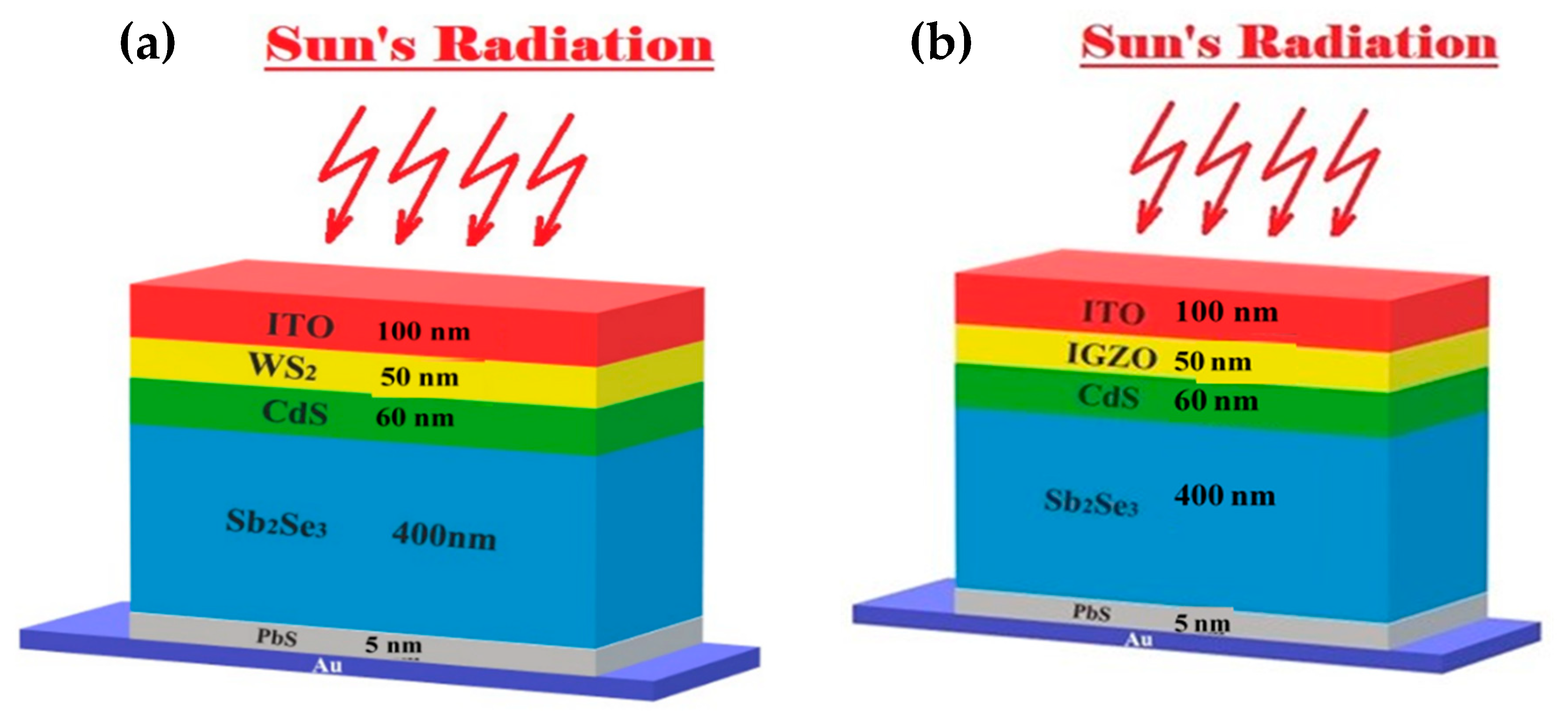
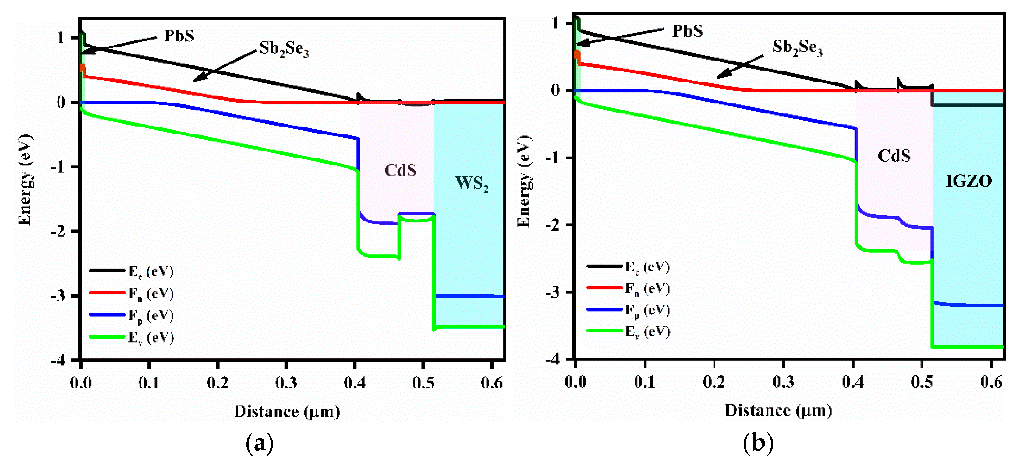
2. Device Structure and Operation

The sun itself can fulfil the never-ending energy requirements of the entire world; however, nearly half of this energy is found in the infrared spectrum [1]. One of the advantages of QDSCs over other conventional solar cell is that the QDSCs makes the energy lie in the region of infrared. In the present work, a four-layered structure is used, namely ETL, the absorber layer, buffer layer, and HTL. The device layer architecture is depicted in Figure 1a,b, which shows all four layers. The WS2 layer is employed as the ETL, as shown in Figure 1a, and it relates to the indium doped tin oxide (ITO) layer, which serves as the front contact through which solar radiation enters the solar cell. Aside from optical transparency, the electrical property is more crucial, as it signifies lower sheet resistance as well as enhanced stability and stickiness. In this aspect, ITO will perform better because it can be developed over a considerably larger area on substrate at lower processing temperatures than FTO coatings, and ITO coatings are much smoother. CdS are used as a buffer layer and antimony triselenide (Sb2Se3) as an absorber layer. The Sb2Se3 absorber layer is coupled with the CdS, which absorbs a huge amount of radiation at the junction of the solar cell device. The back contact of the gold (Au) layer is deposited on the surface of PbS-EDT (HTL). In Figure 1b, the ITO layer is deposited on IGZO (Indium Gallium Tin Oxide) ETL, which acts as the front contact. CdS is used as the electron transport layer, Sb2Se3 as the absorber layer, and the PbS-EDT as the HTL. The calibrated layers are used to analyze the device structure ITO/WS2/CdS/Sb2Se3/PbS-EDT/Au and the modified device contains IGZO as the ETL. The device structure of the modified device structure is ITO/IGZO/CdS/Sb2Se3/PbS/Au. IGZO material has advantages over WS2 material, which include high efficiency, high electron mobility, wide bandgap, eco-friendliness, and cost-effective fabrications.
When solar radiation strikes a solar device, the energy of the radiation is absorbed by the absorber layer, resulting in the generation of an electron-hole pair. Among the different layers, the absorber layer is the most important because it converts electromagnetic radiation energy into electrical energy. To separate the electron-hole pairs produced in the absorber layer, it must be sandwiched between the electron transport layer and the hole transport layer. The PbS HTL in the calibrated device has been treated with 1,2-ethanedithiol (PbS-EDT). Further, with the help of internal electrochemical potential, the generated charge carriers (electrons and holes) are detached from each other. The separated electrons are then moved towards the ETL and holes towards the HTL.
The charge carriers are generated in the absorber layer with the assistance of an external load. The process of light absorption, charge carrier creation (electron and holes), and electron-hole pair separation towards ETL and HTL continues, resulting in continuous energy generation from solar radiation. Table 1, Table 2 and Table 3 represent all the parameters that have been used in the SCAPS-1D simulator for the design of the device.
The Solar Cell Capacitance Simulator (SCAPS-1D) is a solar device simulator application developed at the University of Gent’s Department of Electronics and Information Systems (ELIS). This device includes designing up to seven semiconductor layers, defects at a layer and between the interface of two layers, calculating and plotting the I-V parameters, energy band, PV parameters, J-V, etc. A comparative analysis between the device with WS2 as the ETL and the device with IGZO as the HTL is performed using this SCAPS-1D simulator and is discussed in Section 4 below.
A solution of the semiconductor equations employed in SCAPS is required for this simulation task. It contains Poisson’s equation as well as the electron-hole pair continuity equation, both of which have been extensively solved in the SCAPS simulation.
The Poisson’s equation is as follows [1]:
d dx ε x d ϕ dx = [ p ( x ) n ( x ) + N D   ( x ) N A   ( x ) + p ( x ) n ( x ) ]
where p represents the hole density and ND and NA represent the donor and acceptor densities, respectively. The terns n(x) and n(p) are the trapped electron and hole density, and ε represents the dielectric constant of the medium.
Further, electron and hole continuity in the 1D equation is given as [9,11]:
For electrons:
n x , t t =   1 q J n x + Gn ( x , t ) Rn ( x , t )
For holes:
p x , t t = 1 q J p x   + G p   ( x , t ) R p   ( x , t )
where Jn and Jp are the drift current densities with respect to the concentration of electrons and holes, respectively, n represents the number of electrons present per cubic centimeter, p represents the number of holes per cubic centimeter, q is related to the charge carried by the concentration of carriers, and G and R represents the rate of generation and recombination, respectively.
Carrier density of electrons:
J n = q nu n E   + D n dn dx
Carrier density of holes:
J p = q pu p E   + D p dp dx
where E is the applied electric field and un an up is the mobility of electrons and hole, respectively.
In steady-state condition: n t = 0
Therefore,
1 q J n x   = G n   ( x , t ) + R n   ( x , t )
Substituting the value of J n from the above equation we get:
nu n dE dx + u n E dn dx + D n d 2 n dx 2 = G n x + R n x
Similarly for holes:
pu p dE dx u p E dp dx + D p d 2 p dx 2 = G p x R p x
The SCAPS simulator solves these coupled differential equations and calculates the unknown variables’ values.

3. Result and Discussion

This section is divided into five sub-sections, each of which discusses the favorable outcomes of this work. Each section represents the various aspect of the analysis. The first section includes the outcome of the device, which has been calibrated, and the impact on PV parameters of the device after the replacement of ETL. The second section includes the influence on the performance of both devices when the doping density of HTL is increased. The third section includes the influence of resistance on PV parameters. The fourth section includes the impact of increasing temperature on the performance of the quantum dot solar cell.

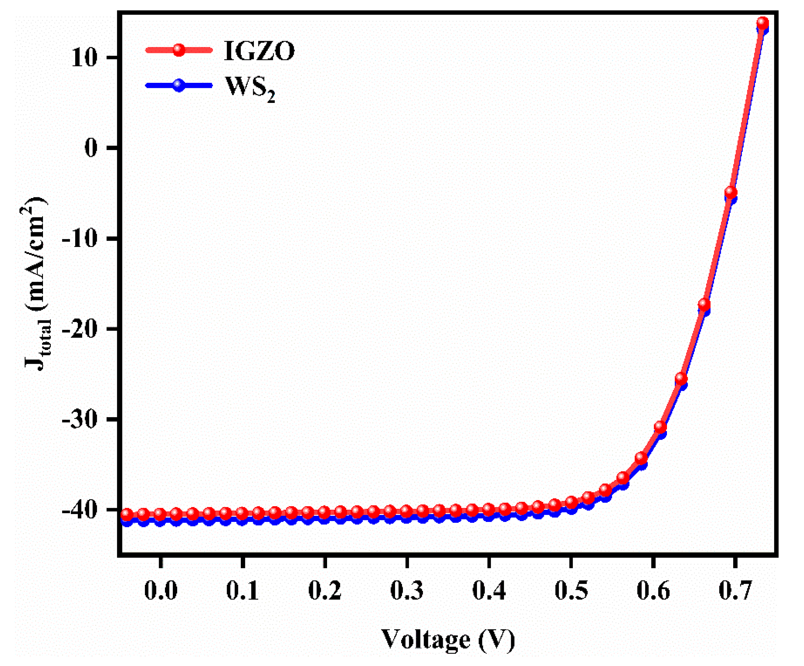
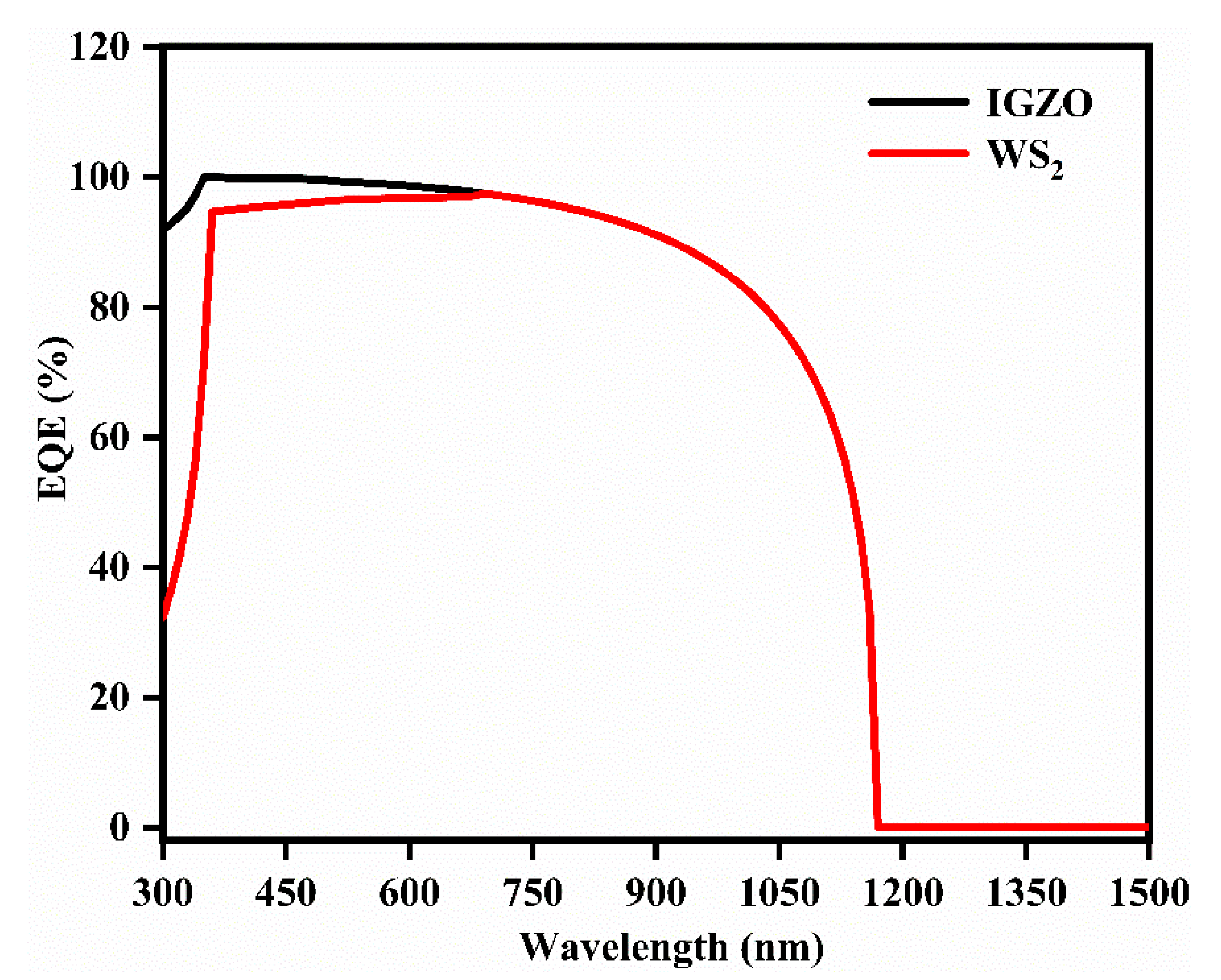
3.1. Influence of Replacement of ETL on Device Performance

The calibration of the device with WS2 as the ETL is examined in this portion of the result, and its replacement with IGZO is carried out. Firstly, a device structure, ITO/WS2/CdS/Sb2Se3/PbS-EDT/Au, is anticipated and calibrated using the simulator. In this device structure, WS2 with a thickness of 50 nm is taken as the ETL. The other three layers include CdS with a thickness of 60 nm, Sb2Se3 having a thickness of 400 nm, and PbS-EDT as the HTL, having 5 nm thickness. After the device has been calibrated, WS2 is replaced with IGZO. To provide a more balanced analysis, the same thickness of IGZO is taken as that of WS2. Further, the donor doping density of both WS2 and IGZO is kept constant. Because doping density has a significant impact on device performance, it has been kept constant for both devices to demonstrate a carrier comparison [24]. An energy band diagram (EBD), EQE, and J-V curve are used to investigate the effect of replacing the electron transport layer, as illustrated in Figure 2, Figure 3 and Figure 4.
The bandgap of a semiconductor material is directly related to the open-circuit voltage (Voc). IGZO has a bandgap of 3.05 eV, which is larger in comparison to the bandgap of WS2, having a bandgap of 1.8 eV. The spike of IGZO is different from that of WS2 because of the replacement of n-type semiconductor material and keeping the p-type material alike. Additionally, by changing the n-type material, the level of the conduction band and valance band will change after p-n junction formation.
Figure 3 represent the current density and voltage (J-V) curve of the WS2 ETL-based device and the new IGZO ETL-based device, keeping the same illumination conditions. The function of any photovoltaic device in a circuit is determined by the J-V curve and hence it is an important and most popular technique. With the help of the J-V curve, various device parameters such as Jsc, Voc, FF, and PCE for both devices can be obtained. Table 4 represents comparative output data for both devices. The Jsc (short-circuit current density) for WS2 ETL- and IGZO ETL-based devices are approximately the same. This slight variation in the value of Jsc indicates that both ETLs are approximately the same in terms of enhancing the working of the absorber layer (Sb2Se3) to absorb light. The Jsc for the IGZO ETL-based device is 41.17 mA/cm2 and for WS2 ETL-based device, the Jsc is 40.52 mA/cm2. The PCE improvement in the IGZO ETL-based device is 20.94%, which is slightly higher than the PCE for the WS2 ETL-based device, whose efficiency is 20.60%. The high Jsc and Voc are attributed to a large number of electron-hole pairs generated within a short time due to the small bandgap of the absorber layer and also due to increased heat production at higher temperatures in the device [9]. Table 3 compares experimental and simulation results. Our findings appear to be in good agreement with those previously reported. Table 3 shows a comparison of simulation and experimental results. Our findings appear to be in good agreement with earlier findings. Differences between simulation and experimental results appear due to their methodology. There is a substantial discrepancy between experimental and simulation results because the experiment is performed directly on the target machine, but software simulation is never performed in this manner. The experiments provide validation of the object’s actual behavior, with varied measurement errors, whereas simulated findings provide insights based on similar computer simulations. Therefore, the main difference between the real object and its theoretical and numerical representations is made, especially when other inaccuracies are drastically reduced. The same explanation has now been incorporated in the revised manuscript.
External quantum efficiency (EQE) is also examined between both WS2 ETL- and IGZO ETL-based devices, and the outcome is represented in Figure 4. An EQE analysis is performed to acknowledge the collection of charge carriers more properly. An IGZO ETL-based device is found to provide slightly higher efficiency in comparison to the device having WS2 as the ETL in the visible range of the electromagnetic spectrum because the reflection of light from the surface of the solar device with IGZO as the ETL is lower compared to the device with WS2 as the ETL. Initially, at 300 nm, the EQE is on the lower side due to front surface recombination [25]. Around this range of wavelength, the EQE of the IGZO ETL-based device is higher compared to the WS2 ETL-based device. Between the range of 400 nm and 700 nm wavelength, the EQE reaches its highest possible value for both devices. From the EQE results, the integrated Jsc values of 40.74 mA/cm2 and 41.57 7 mA/cm2 are estimated for simulated devices based on WS2 ETL and IGZO ETL, respectively. These Jsc values are very close to Jsc values from the J-V results. Further, between 800 and 1200 nm, a reduction in the value of EQE is observed. This is due to the reflection of light from the surface of the device. After 1200 nm of wavelength, both the devices have zero EQE.

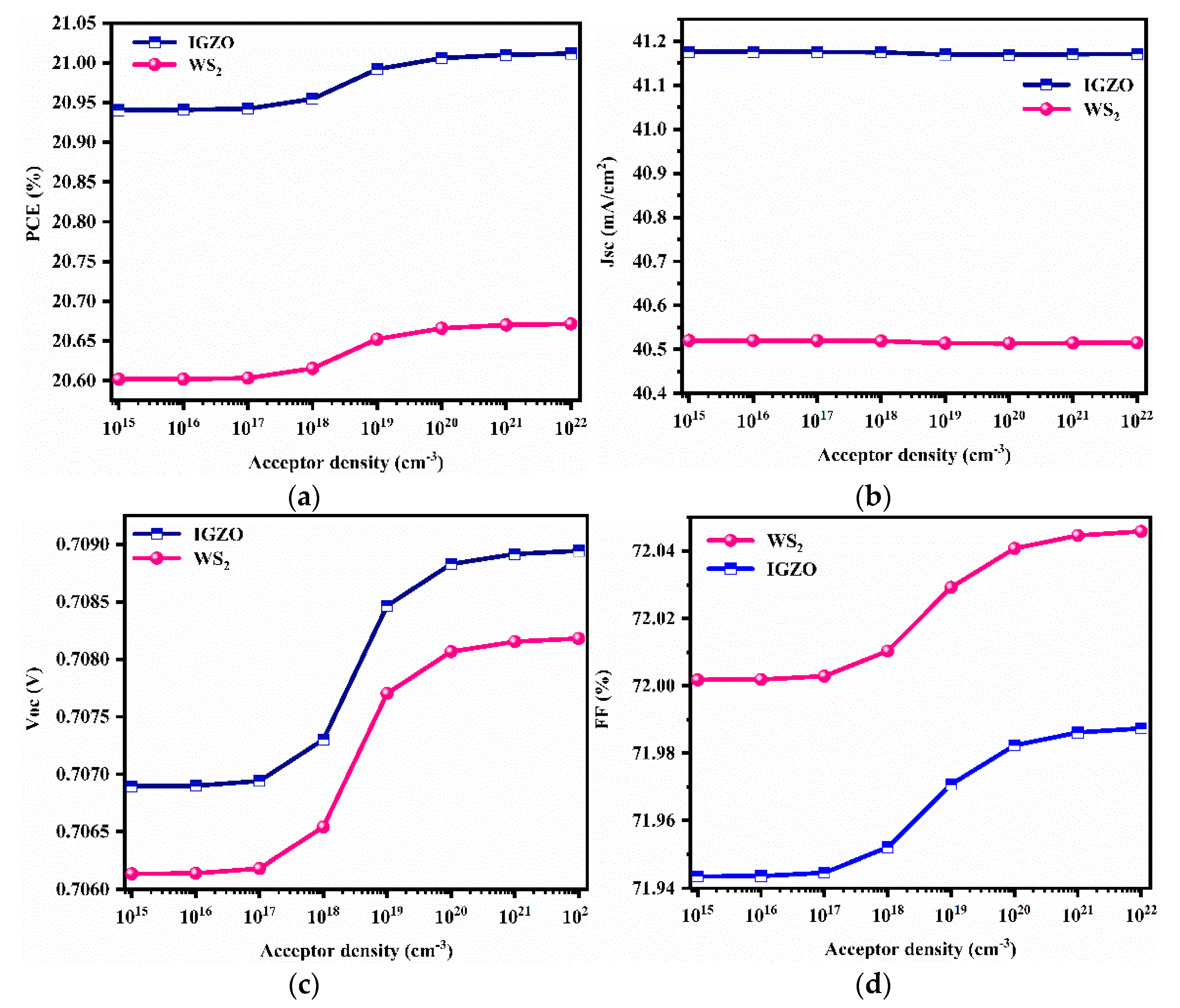
3.2. Comparative Study on the Impact of Doping Density of HTL

In this sub-section of the result, a comparative study on the influence of acceptor density concentration on the device parameters has been performed. The analysis is carried out by changing the doping concentration of PbS HTL for the WS2 ETL-based device and IGZO ETL-based device from 1 × 1015 cm−3 to 1 × 1022 cm−3 in eight equal steps on the log scale. In the SCAPS-1D simulator, these values of photovoltaic parameters were entered in the batch setup option. All other device parameters of the device are kept intact by using a recorder setup, and then the calculation is performed. Figure 5a–d represents the obtained outcome.
From the graphs, it can be observed that by varying the acceptor density of the HTL, the performance of the device with IGZO as the ETL is better than the device with WS2 as the ETL. Figure 5a represents a comparative study for the PCE of both devices. The maximum PCE obtained by the WS2 ETL-based device is 20.67% at 1 × 1022 cm−3, whereas, for the IGZO ETL-based device, the maximum PCE obtained is 20.94% at 1 × 1022 cm−3. In Figure 5b, a comparative study for the Jsc (short circuit current density) is represented. On comparing the values of Jsc for both devices, a very small variation is observed. Further, as the acceptor doping of HTL is increased, an increase in Voc and FF is also observed, as depicted in Figure 5c,d, respectively. The maximum value of Voc and FF obtained by the WS2 ETL-based device is 0.7081 V and 72.04% at 1 × 1022 cm−3, respectively, and the maximum Voc and FF are obtained by the IGZO ETL-based device as 0.7089 V and 71.98% at 1 × 1022 cm−3, respectively. It has been observed that, in all these graphs, the PV parameters such as Voc, PCE, and Jsc of the solar cell device with IGZO as the ETL are slightly higher than the WS2 ETL-based solar device. Thus, the IGZO device is more efficient than the WS2 ETL solar device.

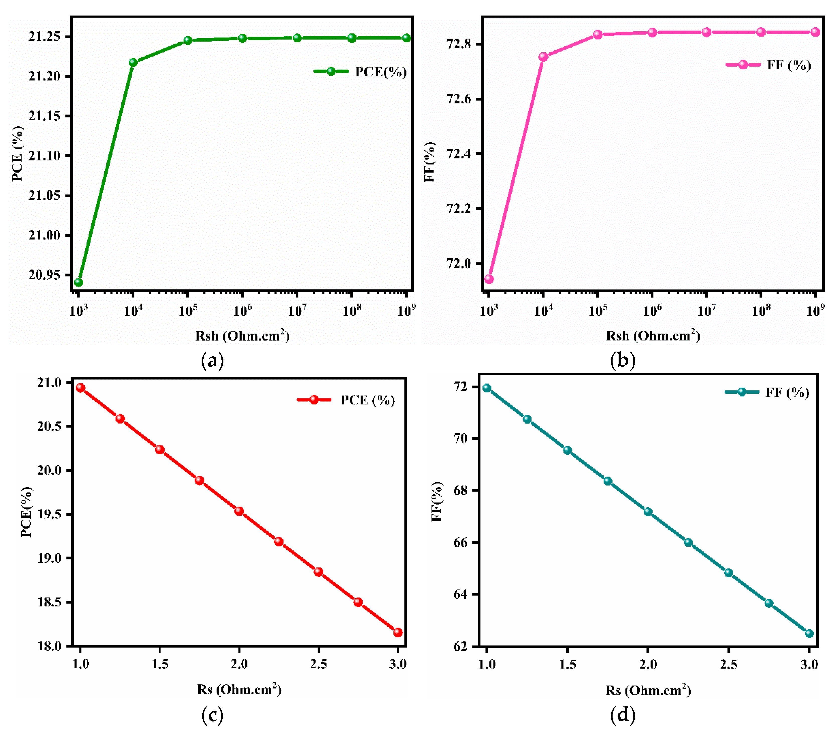
3.3. Comparative Study of the Impact of Series Resistance and Shunt Resistance

The series and shunt resistance have a substantial influence on the device’s performance. The effect of varying series and shunt resistances on the performance of photovoltaic solar cell devices with WS2 as the ETL and the device with IGZO as the ETL has been illustrated in Figure 6a–d. The series and shunt resistances of an ideal solar device are zero and infinity, respectively, but in practice things are considerably different. The parasitic elements that demonstrate losses in solar cells include series and shunt resistance. Shunt resistance is primarily caused by recombination in defect states; as a result, the defect state decreases as the device’s shunt resistance increases [26,29]. In Figure 6a,b, the shunt resistance is represented for the IGZO ETL-based device. The graph shows that the PCE and FF rise to a certain point before levelling off. The best result is attained at 106 ohms.cm2, and the PCE and FF of the device are 21.24% and 72.84%, respectively. The lower PCE is obtained at low shunt resistance. It also degrades device performance by adding another path for photon-generated currents. Figure 6c,d represents the analysis of series resistance for the IGZO based device.
Series resistance decreases the PV parameters of the photovoltaic cell. From the graph, it has been observed that the values of power conversion efficiency and fill factor decrease as we increase the series resistance from 1.0 to 3.0 ohm.cm2. The maximum value of PCE and FF is 20.94% and 71.94% at 1.0 ohm.cm2, respectively.

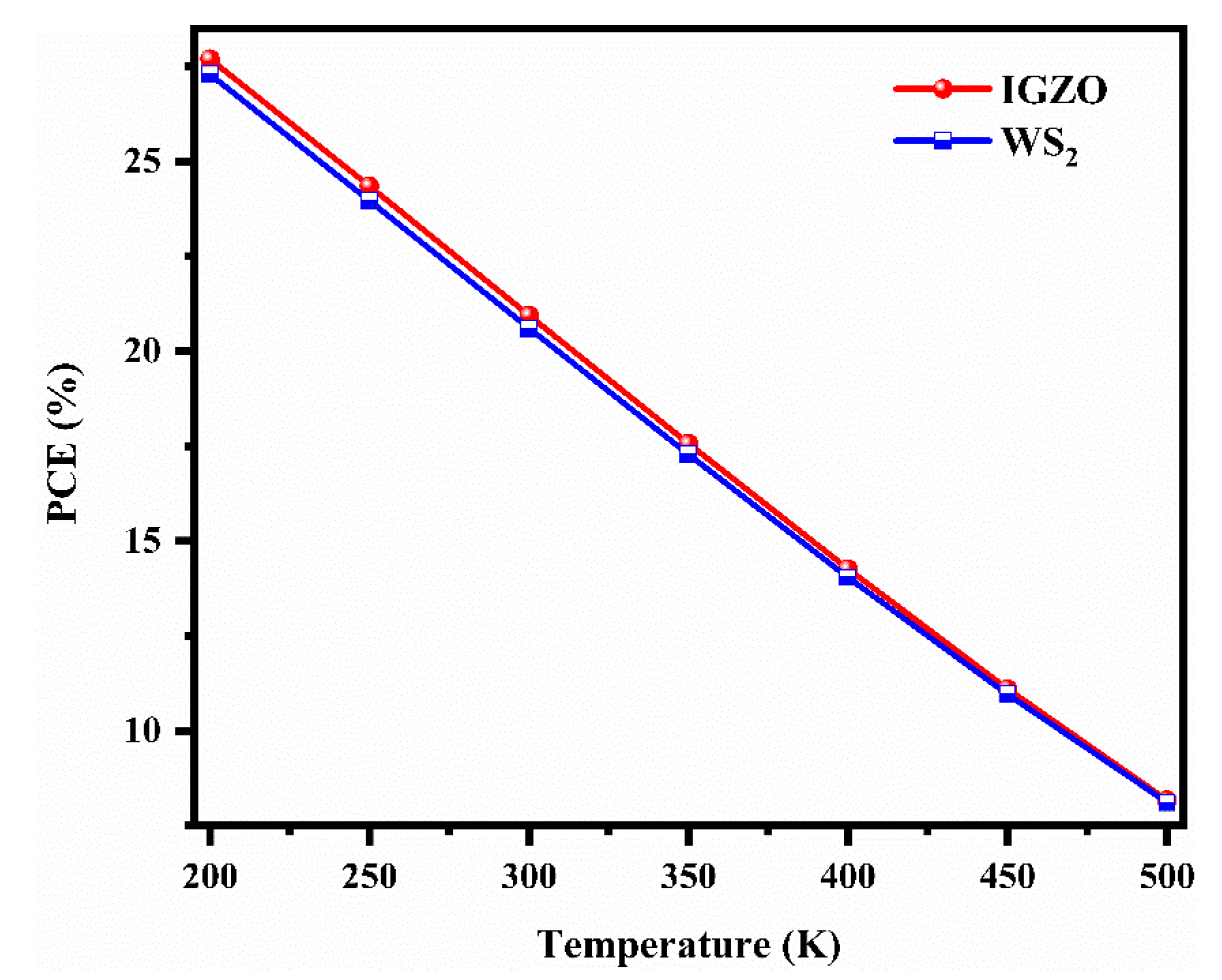
3.4. Comparative Study on the Impact of Increasing Temperature on PCE

Solar cells are installed in open places so that they receive direct sunlight. When sunlight strikes the surface of a solar cell, the temperature of the module rises. In places where the temperature is highest during the summer, the P-V parameters of the solar device are severely impacted. As a result, when it comes to the performance of solar devices, high temperatures are a cause for concern. The performance of the solar cell is appreciable at low temperatures, which deteriorates when the temperature rises [9,30].
Here, the effect of an increase in temperature on the PCE of both devices is discussed. The temperature is varied from 200 K to 500 K, with steps of 50 K, and the corresponding variations are depicted in Figure 7. Across the simulation, the thickness of both ETLs (WS2 and IGZO) is kept constant at 50 nm. It has been observed that with an increase in temperature, the efficiency of the solar cell device starts decreasing. At low temperatures, electrons are at rest and have minimal energy. When electrons are excited by more sunlight (high energy), a solar panel can attain a larger voltage differential. Consequently, solar cells perform better and produce more electricity at low temperatures.
Further, at low temperature, a high value of FF has been observed, but as the temperature increases, the FF decreases due to light-induced degradation. The reverse saturation current increases as the temperature rises. With the increase in temperature, the energy of electrons increases, which in turn decreases the bandgap of both materials. Due to the reverse saturation current, there is a linear decrement in the efficiency of both devices [31]. After gaining energy from the photon, the electron and holes are recombined. The increment in the rate of recombination results in a decrease in the performance of the photovoltaic solar cell.

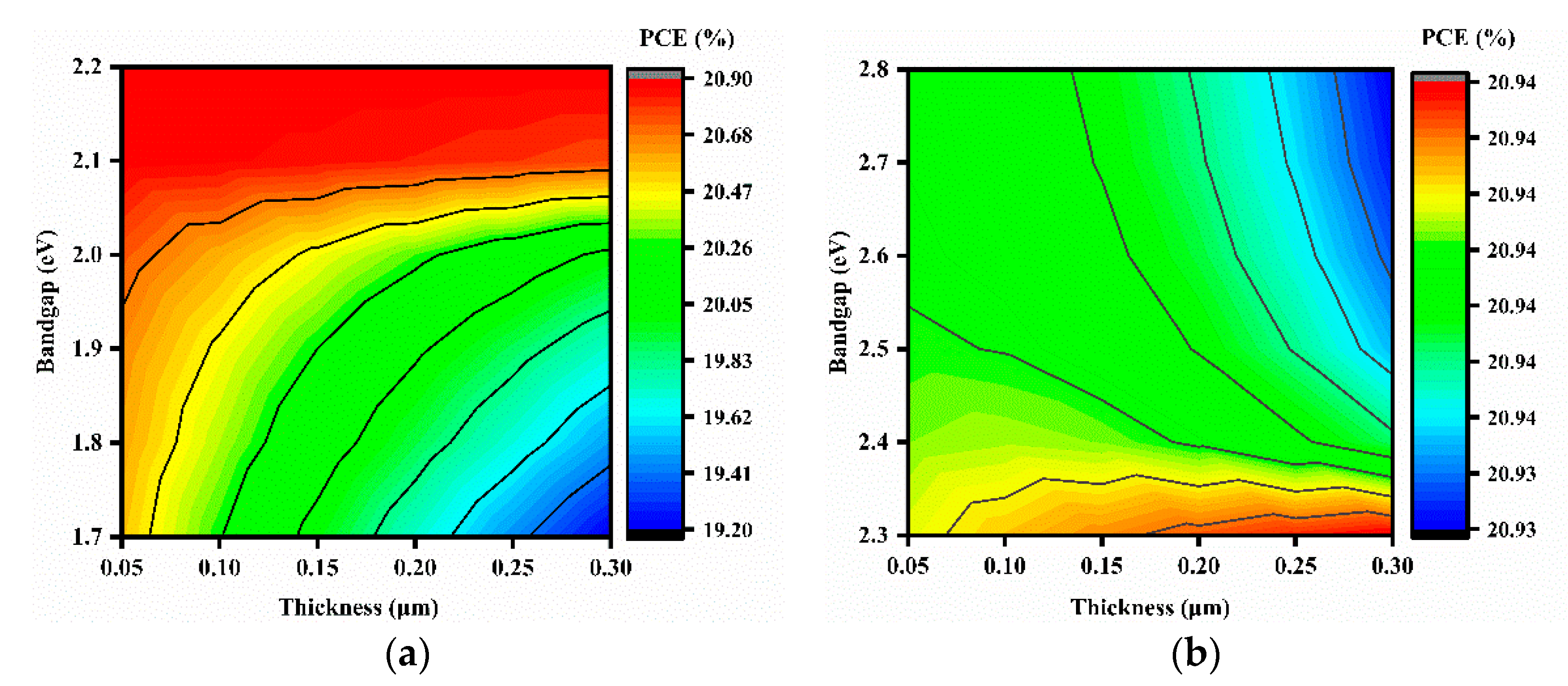
3.5. Contour Plot between Thickness and Bandgap for WS2 and IGZO ETL Based Device

This subsection includes the analysis of the influence of variation of bandgap and thickness on the performance of both devices. Figure 8a,b represents a contour plot between thickness and bandgap for WS2 and IGZO ETLs-based devices. To analyze the impact on the performance of the solar device, the thickness of the ETL layer of both devices has been varied from 0.05 μm to 0.3 μm. From Figure 8a, we could say that the efficiency of the device depends upon its bandgap as well as its thickness. The photon whose energy is larger than the bandgap of the materials may assassinate the electron and create electricity [32,33,34]. Hence, the bandgap of the ETL-based solar cell device is particularly important. However, if a photon with an energy of 1.7 eV collides with an energy cell with 1.1 eV of energy, the excess energy of 0.6 eV is lost as heat [4,35]. Thus, if the bandgap of the material is so high, a huge amount of current (electrons) is not produced because some photons have a huge amount of energy. A bandgap that is too small can create a large number of electrons, but much of the energy is lost as heat.

4. Conclusions

Throughout the entire study, we have used two different ETLs to compare the optimized performance of both devices. The impact of changing various PV parameters on the performance of the photovoltaic device is also investigated. A comparative study between WS2 ETL- and IGZO ETL-based devices was carried out, achieving a PCE of 20.94%. The device structure with WS2 as an ETL is replaced by IGZO, which attains a maximum optimized efficiency of 20.9%. The influence of IGZO on the PV parameters is determined by EBD, J-V curve, and quantum efficiency. The parameter that greatly influences the performance of the solar device is the acceptor concentration of the hole transport layer and the temperature. With the increase in the concentration of acceptor, the efficiency of the solar device also goes on to increases, and at the doping density of 1 × 1022 cm−3, the maximum performance is observed. Further, the impact of both series and shunt resistance is investigated. The optimum value of the series and shunt resistance is taken as 1 ohm·cm2 and 106 ohms·cm2, respectively. Higher temperature decreases the output efficiency of the solar device. Thus, its impact on the performance of the device is also studied, and it is found that the solar device is temperature sensitive. For the appreciable PCE of the device, 300 K is taken as the optimum temperature; with a further increase in the temperature the efficiency of the device decreases. The contour plot between the thickness and bandgap for WS2 and IGZO ETL-based devices is plotted after proper investigation of the HTL, resistance, and temperature. The PCE for the WS2 ETL-based device is 20.60%, while a PCE for the IGZO ETL-based device of 20.94% is obtained. The Jsc, Voc, and FF for WS2 ETL-based devices are 40.52 mA/cm2, 0.706 V, and 72.00%, respectively, and for IGZO-based devices the Jsc, Voc, and FF are 41.17 mA/cm2, 0.706%, and 71.94%, respectively. The study was carried out with the assistance of the SCAPS-1D simulator. The findings of this study could be used to improve the performance of IGZO ETL-based devices by further optimising and analysing the doping densities and interface defects in the ETL and HTL.

Author Contributions

Conceptualization, N.; methodology, N. and S.; validation, S. and D.K.D.; formal analysis, N., S. and D.K.D.; writing—original draft preparation, N.; writing—review and editing, S., D.K.D., P.L. and S.A. All authors have read and agreed to the published version of the manuscript.

Funding

This paper is supported by research funds of Jeonbuk National University in 2022.

Institutional Review Board Statement

Not applicable.

Informed Consent Statement

Not applicable.

Data Availability Statement

Not available.

Conflicts of Interest

The authors declare no conflict of interest.

References

  1. Prasad, S.; Lohia, P.; Dwivedi, D.K. Efficient PbS colloidal quantum dot solar cells employing Cu2O as a hole transport layer. Opt. Quantum. Electron. 2021, 53, 1–14. [Google Scholar] [CrossRef]
  2. Singh, P.K.; Rai, S.; Lohia, P.; Dwivedi, D.K. Comparative study of the CZTS, CuSbS2 and CuSbSe2 solar photovoltaic cell with an earth-abundant non-toxic buffer layer. Sol. Energy 2021, 222, 175–185. [Google Scholar]
  3. Liu, N.; Wang, L.; Xu, F.; Wu, J.; Song, T.; Chen, Q. Recent progress in developing monolithic perovskite/Si tandem solar cells. Front. Chem. 2020, 8, 603375. [Google Scholar] [CrossRef] [PubMed]
  4. Xu, A.F.; Liu, N.; Xie, F.; Song, T.; Ma, Y.; Zhang, P.; Bai, Y.; Li, Y.; Chen, Q.; Xu, G. Promoting thermodynamic and kinetic stabilities of FA-based perovskite by an in situ bilayer structure. Nano Lett. 2020, 20, 3864–3871. [Google Scholar] [CrossRef]
  5. Zhang, L.; Zhao, Y.; Dai, Q. Recent progress in perovskite solar cell: Fabrication, efficiency, and stability. Dev. Sol. Cells 2021, 32, 1–32. [Google Scholar] [CrossRef]
  6. Tripathi, S.; Lohia, P.; Dwivedi, D.K. Contribution to sustainable and environmentally friendly non-toxic CZTS solar cell with an innovative hybrid buffer layer. Sol. Energy 2020, 204, 748–760. [Google Scholar] [CrossRef]
  7. Pandey, R.; Khanna, A.; Singh, K.; Patel, S.K.; Singh, H.; Madan, J. Device simulations: Toward the design of >13% efficient PbS colloidal quantum dot solar cell. Sol. Energy 2020, 207, 893–902. [Google Scholar] [CrossRef]
  8. Sahu, A.; Garg, A.; Dixit, A. A review on quantum dot sensitized solar cells: Past, present and future towards carrier multiplication with a possibility for higher efficiency. Sol. Energy 2020, 203, 210–239. [Google Scholar] [CrossRef]
  9. Rai, N.; Rai, S.; Singh, P.K.; Lohia, P.; Dwivedi, D.K. Analysis of various ETL materials for an efficient perovskite solar cell by numerical simulation. J. Mater. Sci. Mater. Electron. 2020, 31, 16269–16280. [Google Scholar] [CrossRef]
  10. Chen, C.; Wang, L.; Gao, L.; Nam, D.; Li, D.; Li, K.; Zhao, Y.; Ge, C.; Cheong, H.; Liu, H.; et al. 6.5% certified efficiency Sb2Se3 solar cells using PbS colloidal quantum dot film as hole-transporting layer. ACS Energy Lett. 2017, 2, 2125–2132. [Google Scholar] [CrossRef]
  11. Rai, S.; Pandey, B.K.; Dwivedi, D.K. Modelling of highly efficient and low-cost CH3NH3Pb(I1-xClx)3 based perovskite solar cell by numerical simulation. Opt. Mater. 2020, 100, 109631. [Google Scholar] [CrossRef]
  12. Nozik, A.J. Quantum dot solar cells. Phys. E Low-Dimens. Syst. Nanostruct. 2002, 14, 115–120. [Google Scholar] [CrossRef]
  13. Dwivedi, D.K. Numerical modelling for the earth-abundant highly efficient solar photovoltaic cell of non-toxic buffer layer. Opt. Mater. 2020, 109, 110409. [Google Scholar]
  14. Ding, C.; Zhang, Y.; Liu, F.; Kitabatake, Y.; Hayase, S.; Toyoda, T.; Wang, R.; Yoshino, K.; Minemoto, T.; Shen, Q. Understanding charge transfer and recombination by interface engineering for improving the efficiency of PbS quantum dot solar cells. Nanoscale Horiz. 2018, 3, 417–429. [Google Scholar] [CrossRef]
  15. Dwivedi, D.K. Theoretical investigation on the enhancement of output performance of CZTSSe based solar cell. Sol. Energy 2019, 193, 442–451. [Google Scholar]
  16. Kramer, I.J.; Sargent, E.H. The architecture of colloidal quantum dot solar cells: Materials to devices. Chem. Rev. 2014, 114, 863–882. [Google Scholar] [CrossRef]
  17. Gao, W.; Zhai, G.; Zhang, C.; Shao, Z.; Zheng, L.; Zhang, Y.; Yang, Y.; Li, X.; Liu, X.; Xu, B. Towards understanding the initial performance improvement of PbS quantum dot solar cells upon short-term air exposure. RSC Adv. 2018, 8, 15149–15157. [Google Scholar] [CrossRef] [Green Version]
  18. Guo, Y.; Lei, H.; Xiong, L.; Li, B.; Chen, Z.; Wen, J.; Yang, G.; Li, G.; Fang, G. Single phase, high hole mobility Cu2O films as an efficient and robust hole transporting layer for organic solar cells. J. Mater. Chem. A 2017, 5, 11055–11062. [Google Scholar] [CrossRef]
  19. Hima, A.; Lakhdar, N.; Saadoune, A. Effect of Electron Transporting Layer on Power Conversion Efficiency of Perovskite-based Solar Cell: Comparative Study. J. Nano Electron. Phys. 2019, 11, 1–3. [Google Scholar] [CrossRef]
  20. Hossain, M.I.; Alharbi, F.H.; Tabet, N. Copper oxide as inorganic hole transport material for lead halide perovskite-based solar cells. Sol. Energy 2015, 120, 370–380. [Google Scholar] [CrossRef]
  21. Kannan, N.; Vakeesan, D. Solar energy for the future world: A review. Renew. Sustain. Energy Rev. 2016, 62, 1092–1105. [Google Scholar] [CrossRef]
  22. Khaled, S.A.; Kate, R.S.; Deokate, R.J. A review on energy economics and the recent research and development in energy and the Cu2ZnSnS4 (CZTS) solar cells: A focus towards efficiency. Sol. Energy 2018, 169, 616–633. [Google Scholar]
  23. Kirmani, A.R.; Sheikh, A.D.; Niazi, M.R.; Haque, M.A.; Liu, M.; de Arquer, F.P.G.; Xu, J.; Sun, B.; Voznyy, O.; Gasparini, N.; et al. Overcoming the Ambient Manufacturability-Scalability-Performance Bottleneck in Colloidal Quantum Dot Photovoltaics. Adv. Mater. 2018, 30, 1801661. [Google Scholar] [CrossRef] [PubMed] [Green Version]
  24. Li, L.; Yang, X.; Gao, J.; Tian, H.; Zhao, J.; Hagfeldt, A.; Sun, L. Highly efficient CdS quantum dot sensitized solar cells based on a modified polysulfide electrolyte. J. Am. Chem. Soc. 2011, 133, 8458–8460. [Google Scholar] [CrossRef]
  25. Ning, Z.; Zhitomirsky, D.; Adinolfi, V.; Sutherland, B.; Xu, J.; Voznyy, O.; Maraghechi, P.; Lan, X.; Hoogland, S.; Ren, Y.; et al. Graded doping for enhanced colloidal quantum dot photovoltaics. Adv. Mater. 2013, 25, 1719–1723. [Google Scholar] [CrossRef]
  26. Rühle, S.; Shalom, M.; Zaban, A. Quantum-dot-sensitized solar cells. ChemPhysChem 2010, 11, 2290–2304. [Google Scholar] [CrossRef]
  27. Xing, M.; Zhang, Y.; Shen, Q.; Wang, R. Temperature-dependent photovoltaic performance of TiO2/PbS heterojunction quantum dot solar cells. Sol. Energy 2020, 195, 1–5. [Google Scholar] [CrossRef]
  28. Zhang, X.; Santra, P.K.; Tian, L.; Johansson, M.B.; Rensmo, H.; Johansson, E.M. Highly efficient flexible quantum dot solar cells with improved electron extraction using MgZnO nanocrystals. ACS Nano 2017, 11, 8478–8487. [Google Scholar] [CrossRef]
  29. Du, J.; Du, Z.; Hu, J.S.; Pan, Z.; Shen, Q.; Sun, J.; Long, D.; Dong, H.; Sun, L.; Zhong, X.; et al. Zn–Cu–In–Se quantum dot solar cells with a certified power conversion efficiency of 11.6%. J. Am. Chem. Soc. 2016, 138, 4201–4209. [Google Scholar] [CrossRef]
  30. Smith, A.M.; Nie, S. Semiconductor nanocrystals: Structure, properties, and bandgap engineering. Acc. Chem. Res. 2010, 43, 190–200. [Google Scholar] [CrossRef] [Green Version]
  31. Song, X.; Ji, X.; Li, M.; Lin, W.; Luo, X.; Zhang, H. A Review on Development Prospect of CZTS Based Thin Film Solar Cells. Int. J. Photoenergy 2014, 2014, 613173. [Google Scholar] [CrossRef]
  32. Tang, J.; Kemp, K.W.; Hoogland, S.; Jeong, K.S.; Liu, H.; Levina, L.; Furukawa, M.; Wang, X.; Debnath, R.; Cha, D.; et al. Colloidal-quantum-dot photovoltaics using atomic-ligand passivation. Nat. Mater. 2011, 10, 765–771. [Google Scholar] [CrossRef]
  33. Teimouri, R.; Mohammadpour, R. Potential application of CuSbS2 as the hole transport material in perovskite solar cell: A simulation study. Superlattices Microstruct. 2018, 118, 116–122. [Google Scholar] [CrossRef]
  34. Vallisree, S.; Thangavel, R.; Lenka, T.R. Theoretical investigations on the enhancement of photovoltaic efficiency of nanostructured CZTS/ZnS/ZnO based solar cell device. J. Mater. Sci. Mater. Electron. 2018, 29, 7262–7272. [Google Scholar] [CrossRef]
  35. Chaudhary, P.; Verma, A.; Mishra, A.; Yadav, D.; Pal, K.; Yadav, B.C.; Kumar, E.R.; Thapa, K.B.; Mishra, S.; Dwivedi, D.K. Preparation of carbon quantum dots using bike pollutant soot: Evaluation of structural, optical and moisture sensing properties. Phys. E Low-Dimens. Syst. Nanostruct. 2022, 139, 115174. [Google Scholar] [CrossRef]
Figure 1. Schematic of the device structure of (a) WS2 and (b) IGZO ETL-based devices.
Solar 02 00020 g001
Figure 2. Energy band diagram of (a) device having WS2 and (b) device having IGZO as ETLs.
Solar 02 00020 g002
Figure 3. J-V Curve of WS2 and IGZO ETL-based solar cell.
Solar 02 00020 g003
Figure 4. External Quantum Efficiency of WS2 ETL- and IGZO ETL-based solar device.
Solar 02 00020 g004
Figure 5. (ad): Influence of variation in acceptor density (HTL Layer) on P-V parameters (a) PCE, (b) Jsc, (c) Voc, and (d) FF for WS2 ETL- and IGZO ETL-based devices.
Solar 02 00020 g005
Figure 6. (ad): Impact of resistance variation on (a) power conversion efficiency (PCE) for shunt resistance and (b) fill factor (FF) for shunt resistance; (c) PCE for series resistance and (d) FF for series resistance.
Solar 02 00020 g006
Figure 7. Impact of increasing temperature on the QDSC performance.
Solar 02 00020 g007
Figure 8. Contour plot between thickness and bandgap for WS2 (a) and IGZO (b) ETLs-based device.
Solar 02 00020 g008
Table 1. The parameters of different layers of solar photovoltaic devices were utilized to conduct the investigation [2,7,9,10,15].
ParametersITOWS2IGZOCdSSb2Se3HTL
Thickness (nm)255050604005
Eg (eV)3.51.83.052.41.061.2
Affinity for Electrons (eV)4.03.954.1644.154.0
Dielectric permittivity9.013.610101910
Mobility of electrons, μe (cm2/Vs)2010015100100.01
Mobility of holes, μh (cm2/Vs)101000.12510.01
ND (cm−3)1 × 10181.0 × 10181 × 10181.1 × 1018-1 × 10¹⁵
NA (cm−3)----2 × 10141.00 × 1015
Nt (cm−3)101410151014101410141.0 × 1014
Nc (cm−3)2.2 × 10182.2 × 10175 × 10182.2 × 10181.0 × 10181.0 × 1019
Nv (cm−3)1.8 × 10182.2 × 10165 × 10181.8 × 10191.8 × 10201.8 × 1013
Thermal velocity of e (cm/s)107107107107107107
The thermal velocity of holes (cm/s)1.0 × 1071.0 × 1071.0 × 1071.0 × 1071.0 × 1071.0 × 107
Table 2. The CdS trap state parameters for SCAPS simulation [10,15].
ParametersDefect 1
Type of defectSingle acceptor (−/0)
Et (eV) above Ev1.2
Cross Section Area of e (cm2)10−17
Cross Section Area of the hole (cm2)10−12
Nt (cm−3)1.0 × 10⁻¹⁸
Table 3. The Sb2Se3 trap state parameters for SCAPS simulation 10].
ParametersDefect
Type of defectNeutral
Et (eV) above Ev0.55
Cross Section Area of e (cm2)10−13
Cross Section Area of hole (cm2)1.5 × 10⁻¹⁴
Nt (cm−3)1.6 × 10⁻¹⁵
Table 4. Photovoltaic parameters of the device having WS2 as ETL, IGZO as ETL, and the certified device [10].
DeviceJsc (mA/cm2)Voc (V)FF (%)PCE (%)Reference
WS2 ETL-based solar device40.52 mA/cm20.706 V72.00%20.60%This work
IGZO ETL-based solar device41.17 mA/cm20.706 V71.94%20.94 ± 0.62%This work
PbS CQD HTL (certified) 25.5 mA/cm20.427 V59.3%6.50%[10]
Cu2O HTL-based QDSC device24.60 mA/cm20.7559 V73.76%13.72%[1]
Calibrated device with MZO ETL24.51 mA/cm20. 633 V60.8%9.43%[7]
TiO2 ETL-based device24.46 mA/cm20. 635 V63.8%9.87%[27]
MZO-NC ETL-based device24.5 mA/cm20.62 V62.0%9.41%[7,28]
QDSCs(Certified value)25.25 mA/cm20.739 V62.2%11.61%[29]
Publisher’s Note: MDPI stays neutral with regard to jurisdictional claims in published maps and institutional affiliations.

