
Integrated Optics: Platforms and Fabrication Methods


Institute of Microelectronics and Optoelectronics, Warsaw University of Technology, Koszykowa 75, 00-662 Warszawa, Poland
Encyclopedia 2023, 3(3), 824-838; https://doi.org/10.3390/encyclopedia3030059
Submission received: 22 May 2023
/
Revised: 7 June 2023
/
Accepted: 27 June 2023
/
Published: 28 June 2023
(This article belongs to the Section Engineering)
Definition
:Integrated optics is a field of study and technology that focuses on the design, fabrication, and application of optical devices and systems using integrated circuit technology. It involves the integration of various optical components, such as waveguides, couplers, modulators, detectors, and lasers, into a single substrate. One of the key advantages of integrated optics is its compatibility with electronic integrated circuits. This compatibility enables seamless integration of optical and electronic functionalities onto the same chip, allowing efficient data transfer between optical and electronic domains. This synergy is crucial for applications such as optical interconnects in high-speed communication systems, optical sensing interfaces, and optoelectronic integrated circuits. This entry presents a brief study on some of the widely used and commercially available optical platforms and fabrication methods that can be used to create photonic integrated circuits.
1. Introduction
Integrated optics refers to the field of study and technology that involves the integration of various optical components, such as waveguides (WGs), lasers, modulators, detectors, and filters, onto a single photonic integrated circuit (PIC) [1,2]. It aims to miniaturize and integrate optical functions and devices onto a single platform, similar to how electronic circuits are integrated onto a microchip [3]. The major benefit of integrated optics is its ability to manipulate and control light signals on a small scale, leading to compact and highly efficient optical systems. By integrating different optical components onto a chip, it becomes possible to perform complex optical operations, such as signal generation, modulation, amplification, routing, and detection, all of which occur within a compact and stable platform.
Optical signals have a much higher bandwidth and can transmit data at significantly higher speeds than electrical signals [4,5]. These features make integrated optics particularly advantageous in high-speed data communication and interconnected applications. Optical communication systems can transmit large amounts of data over long distances with low signal degradation, enabling faster and more efficient data transfer. Integrated optics can achieve low signal losses, especially when using WGs made of low-loss materials, such as silicon or indium phosphide. This feature enables long-distance transmission without significant degradation of the optical signal. In contrast, electrical signals suffer from losses due to resistance, capacitance, and inductance, especially at higher frequencies [6,7].
Optical signals are immune to electromagnetic interference (EMI), which can disrupt or degrade electrical signals in electronic circuits. This benefit makes integrated optics more suitable for applications where EMI is a concern, such as those operating in high-noise environments or near electromagnetic radiation sources. Integrated optics allows the integration of multiple optical components and functionalities onto a single chip or substrate. This integration reduces the size, weight, and complexity of optical systems compared to traditional electronic circuits [8,9]. It also empowers the development of compact, highly integrated photonic circuits, making them suitable for applications where space is limited or portability is important.
Optical signals can carry a vast amount of data simultaneously due to their high bandwidth [10,11]. This property is crucial in applications that require high data capacity, such as data centers, telecommunications networks, and high-performance computers. Integrated optics provides a scalable and efficient solution for handling large data volumes [12,13]. It is important to note that integrated optics and electronic circuits are often complementary technologies, and their selection depends on the specific application requirements. Some applications may benefit from the integration of both optics and electronics, leveraging the strengths of each technology for optimal performance and functionality.
The main building block of integrated optics is the WG, which is a structure that guides and confines light within a material, typically a semiconductor or a dielectric [1]. WGs can be fabricated using various techniques, including lithography, etching, and deposition processes. The basic principle behind an optical WG is total internal reflection, which occurs when light travels from a medium with a higher refractive index to a medium with a lower refractive index at an angle larger than the critical angle. This technique permits the light to be confined within the WG structure. The dimensions of the WG, such as the width, height, and thickness, are designed to ensure that the light remains trapped and guided along the desired path. The refractive index contrast between the core and the cladding layers of the WG is an imperative parameter for determining the dimensions of the WG [14]. A higher refractive index contrast enables better confinement and tighter light propagation within the WG structure. Thus, the dimensions of the WG will vary depending on the refractive indices of the core and cladding materials.
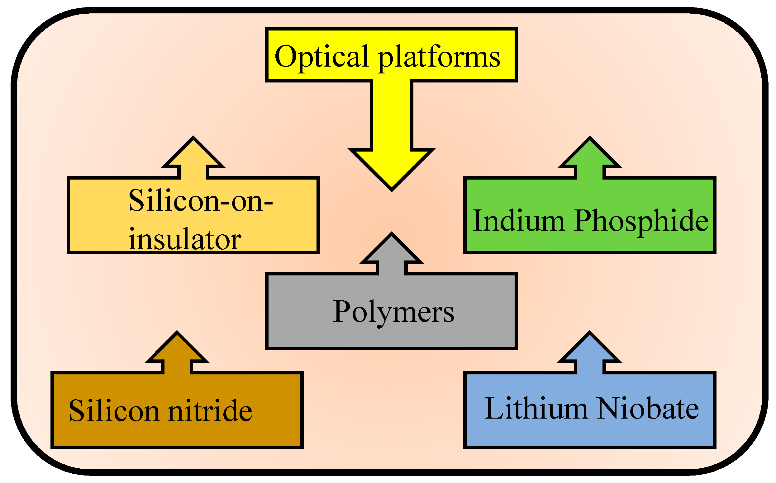
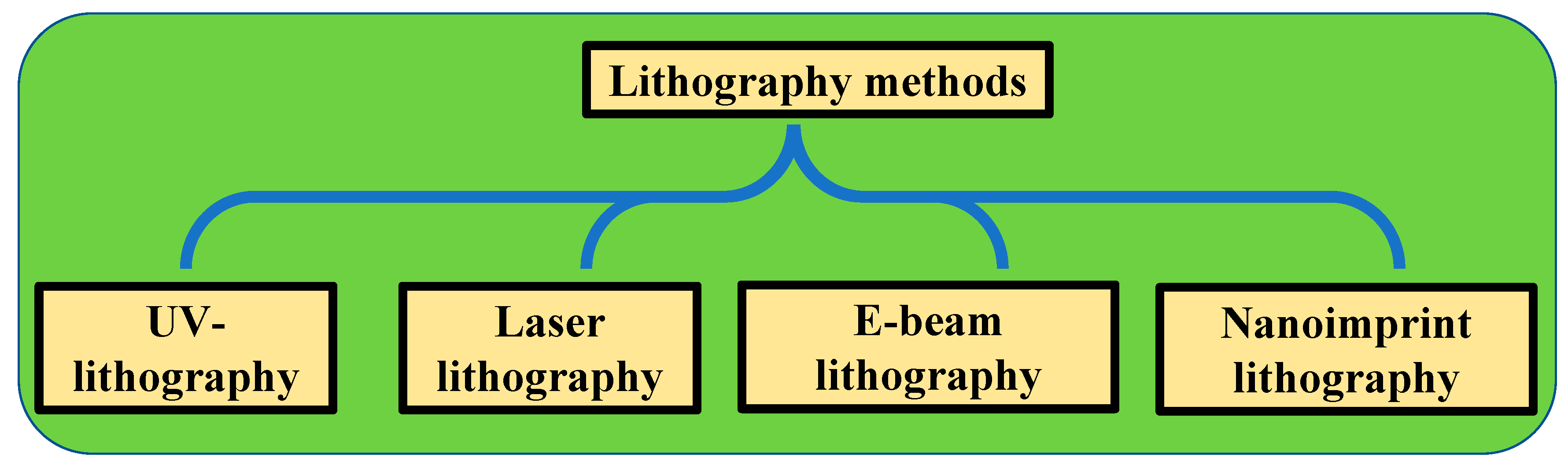
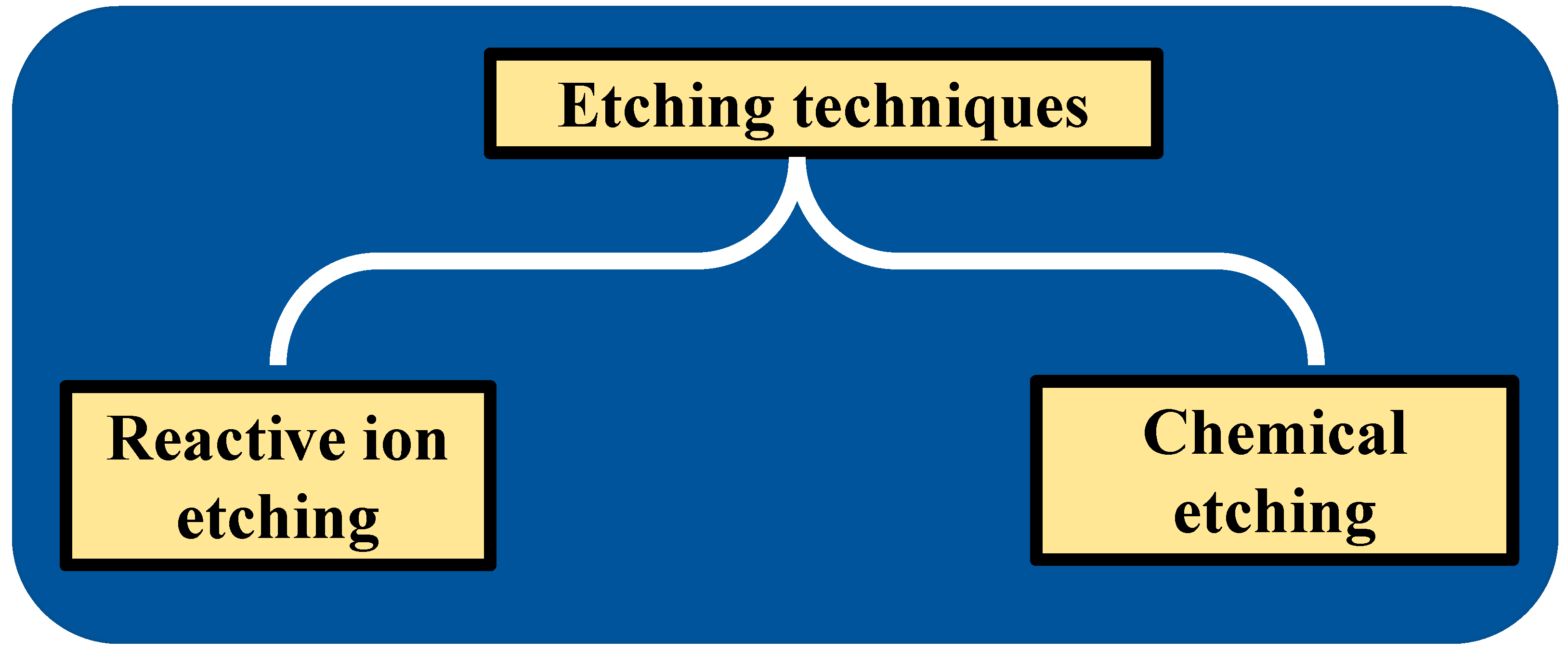
This entry briefly describes the most widely used optical platforms, such as silicon-on-insulator (SOI), indium phosphide (InP), polymers, silicon nitride (Si3N4), and lithium niobate (LiNbO3). Lithography plays a crucial role in defining the resolution of a waveguide in integrated photonic devices. Thus, it is important to choose an appropriate patterning method for the realization of the best possible features of the photonic device. The most used lithography techniques, which include ultra-violet lithography (UVL), laser lithography (LL), electron beam lithography (EBL), and nanoimprint lithography (NIL) are discussed. In the end, reactive ion etching (RIE) and chemical wet etching methods are presented for the fabrication of the WG structures. The entry then ends with the concluding remarks.
2. Integrated Optics Platforms
Several optical platforms are used for integrated optics, with each platform offering different advantages and characteristics [14,15]. The most widely used optical platforms studied in this entry are shown in Figure 1.
2.1. Silicon Photonics
Silicon photonics is a widely adopted platform for integrated optics due to its compatibility with complementary metal-oxide-semiconductor (CMOS) processes [16]. It leverages the existing infrastructure of the semiconductor industry and enables the integration of both electronic and photonic components onto the same chip [17,18,19]. Silicon photonics offers low-cost manufacturing, high device density, and compatibility with existing electronics, making it suitable for applications in data centers, telecommunications, and optical interconnects [18,20,21].
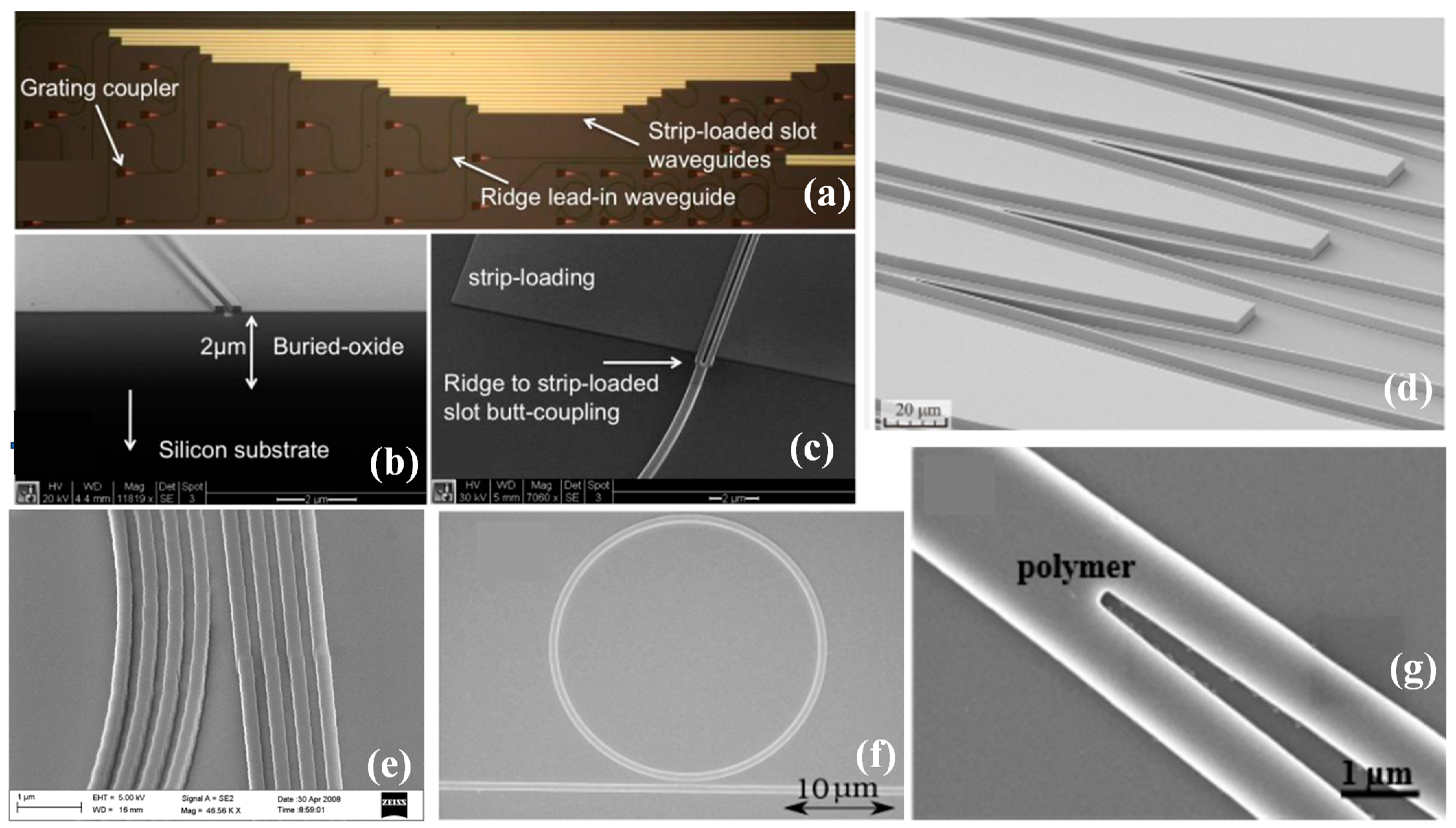
A novel class of modulators with extraordinarily large bandwidths and extremely low driving voltages was recently developed using silicon slot WGs with electro-optic polymer coatings [22]. In order to make these devices feasible, optical insertion losses must be reduced. A strip-loaded slot WG was used to demonstrate the first measurements of low-loss WGs that are physically appropriate for high bandwidth slot WG modulators. With a slot size of 200 nm and a whole silicon thickness of roughly 220 nm, WG loss for undoped WGs of 6.5 ± 0.2 dB/cm was attained at an operational wavelength of ~1550 nm. A diagram of the runout structure geometry is shown in Figure 2a. SEM images of the slot WG and ridge WG to strip-loaded slot WG are shown in Figure 2b,c, respectively [22].
2.2. Indium Phosphide
Indium Phosphide (InP) is a compound semiconductor material that exhibits excellent optical properties, especially in the infrared wavelength range [16]. InP-based integrated optics platforms enable the creation of high-performance devices, including lasers, modulators, detectors, and amplifiers. InP is particularly suitable for applications such as long-haul telecommunications, optical fiber networks, and high-speed optical communication systems [27].
In InP-based optoelectronics, WG structures are frequently formed using chlorine techniques. The typical substrate temperature range for ICP etching of InP in a Cl2-based plasma is 150–200 °C. This range is necessary because low-volatility InClx components created during the etching process and deposited onto the substrate at inadequate temperatures might result in the creation of defects and make the formation of WG structures impossible. The use of chlorine methods is constrained by the requirement to warm the substrate. In [23], it is explained that to ICP etch an InP/InGaAsP heterostructure involves using a Cl2/Ar/N2 gas combination, as shown in Figure 2d [23]. The cyclic etching of the heterostructure without prior heating is a characteristic of the developed approach. At a standard temperature, the etching process begins. The angle of inclination of the WG’s sidewalls reached 88.8° at an etching depth of more than 4.5 µm while using the best etching mode. Additionally, the surface roughness was under 30 nm. Regarding the SiNx mask, the etching procedure had a selectivity of 9. The created etching technique was used to test integrated WG components. The developed active integrated WG with a width of 2 µm showed an optical loss of about 11 ± 1.5 dB/cm at 1550 nm. The designed Y- and MMI-splitters’ insertion loss was 0.8 dB or less [23].
2.3. Silicon Nitride (Si3N4)
Silicon nitride (Si3N4) photonics is an emerging field of research and technology that focuses on the use of Si3N4 as a material platform for the manipulation and control of light at the photonic level [28]. The WGs based on this platform can be combined with other photonic components, such as couplers, splitters, modulators, and detectors, to create highly integrated photonic circuits on a single chip. These circuits enable complex functionalities, such as signal routing, modulation, and detection, in compact and scalable form factors.
In the past 10 years, Si3N4 has gained popularity as a material for manufacturing PICs. It is praised for its broadband transparency, compatibility with CMOS fabrication techniques, and high optical bandgap that prevents two-photon absorption. Current manufacturing techniques, however, force users to pick between low thermal budgets and low losses, which is not the best situation given that both options are required to support a variety of applications. Deuterated silicon nitride (SiNx:D), which constitutes SiNx films generated using deuterated precursors rather than normal hydrogenated precursors, has recently been used to construct PICs. As a result, parasitic silicon–hydrogen and nitrogen-hydrogen bonds that were previously responsible for material absorption near the 1.55 m telecommunications bands are no longer present. Low-loss PICs are then realized using a low temperature, back-end-of-line CMOS-compatible fabrication plasma-enhanced chemical vapor deposition process. Both linear and non-linear applications have shown promise for use with these devices, and the platform may play a key role in the development of extremely efficient circuits with integrated photonics and electronics components [29].
Si3N4 is a transparent material with excellent optical properties, making it well-suited to a variety of photonic applications. One of the key advantages of Si3N4 photonics is its compatibility with standard silicon fabrication processes, which allows for the integration of photonics with CMOS technology. This integration enables the development of highly compact and scalable photonic devices and circuits using a silicon chip [30,31,32]. Si3N4 WGs are used in optical communication systems for signal transmission, routing, and wavelength division multiplexing (WDM) [33]. They can guide and confine light over long distances while minimizing losses, enabling high-speed data transmission. These WGs can be used for various sensing applications, including biochemical sensing, environmental monitoring, and gas sensing. The evanescent field of light propagates through the WG interacts with the surrounding environment, allowing sensitive detection of changes in refractive indices or molecular interactions [34].
They possess strong non-linear optical properties, making them useful for applications such as frequency conversion, parametric amplification, and optical signal processing. Non-linear effects can be exploited to generate new wavelengths, modify the spectral content of optical signals, and perform all-optical signal processing operations [35].
These WGs are compatible with the integration of quantum emitters, such as quantum dots or color centers, enabling the creation of on-chip quantum photonic devices. These devices are crucial for applications in quantum information processing, quantum communication, and quantum sensing [36]. Si3N4 WGs can also be used for on-chip spectroscopic analysis [32]. By incorporating specific functional elements, such as grating couplers or resonators, the WGs can interact with light at specific wavelengths, allowing the detection and analysis of chemical compounds or biomolecules.
The first example of ring resonators based on vertical WGs that have multiple slots made of Si3N4 is provided [24]. The SEM image of segment of the ring resonator based on multi-slot WG is shown in Figure 2e [24]. At a wavelength of 1.3 µm, the design, construction, and measurement of multiple-slot WG ring resonators with various coupling distances and ring radii (70 µm, 90 µm, and 110 µm) were performed. For TE and TM polarization, quality factors of 6100 and 16,000, respectively, were attained.
2.4. Lithium Niobate
Lithium Niobate (LiNbO3) is a crystal with excellent electro-optic properties, making it suitable for applications that require the modulation of light signals. LiNbO3-based integrated optics platforms are used in various devices, including electro-optic modulators, switches, and frequency converters [37]. They find applications in telecommunications, fiber-optic networks, and optical signal processing [38]. LitNbO3 exhibits strong non-linear optical properties, making it suitable for applications in non-linear optics. LiNbO3 WGs can be used to generate and manipulate various non-linear optical effects, including frequency conversion, second harmonic generation, parametric amplification, and optical parametric oscillation [39].
One of the key properties of lithium niobate is its strong electro-optic effect, which is known as the Pockels effect. By applying an electric field to the WG, the refractive index of the material can be modulated, enabling efficient electro-optic modulation of light. LiNbO3 WGs are commonly used in the development of high-speed electro-optic modulators for optical communication systems [40]. LiNbO3 WGs now have applications in the emerging field of quantum photonics. They can be used to generate and manipulate single photons and entangled photon pairs, which are essential for various quantum technologies, such as quantum communication, quantum cryptography, and quantum computing [41].
Lithium niobate on insulator (LNOI) photonics has the potential to fuse high complexity, which is made possible by high contrast WGs with exceptional non-linear characteristics of LiNbO3 [25]. Its usefulness is restricted, however, because of manufacturing difficulties that led to high-loss and sidewall angled WGs. It is alleged that LNOI single mode WGs have an extremely low propagation loss of 0.4 dB/cm and a sidewall angle of 75°. These findings pave the way for a highly effective photonic platform with applicatiobns in high-speed communications and quantum technologies. The SEM image of the ring resonator structure formed on LNOI platform is shown in Figure 2f [25].
2.5. Polymers
Polymer WGs are fabricated using organic materials, such as polymers and copolymers, that possess good optical properties [42]. Polymer-based integrated optics platforms offer advantages like low-cost fabrication, flexibility, and ease of integration [43]. They are often used in applications in which cost-effective solutions and low-loss transmission are important, such as consumer electronics, short-reach optical communication, and sensing systems [14]. These WGs can be easily integrated with other optical components, such as lasers, detectors, modulators, and multiplexers. This compatibility facilitates the development of compact and multifunctional photonic devices and systems [44,45,46].
Certain polymer materials used for WGs, such as biocompatible polymers or polymers with specific surface modifications, can be used for bio-photonics applications [47]. These WGs can be employed in areas like biomedical sensing, lab-on-a-chip devices, or optogenetics, where interaction with biological systems is required [48]. Polymer WGs are highly flexible and can be simply shaped into various forms, allowing the creation of complex optical circuits and integration with other devices. This flexibility is mainly advantageous for applications that require bending or twisting, such as wearable devices or biomedical applications [49].
A polymer slot WG Young interferometer covered with an Al2O3/TiO2 bilayer is presented. This method makes it possible for the polymer WG’s dimensions to be relaxed, which makes it easier to fabricate the structure with a precision of 50 nm [26]. Atomic layer deposition (ALD) was used to cover the layers. Using the interferometric structure as a bulk refractive index sensor operating at 975 nm wavelength to detect an ethanol water solution, the device’s viability was examined. With a sensing length of just 800 µm, a refractive index change of 1 × 10⁻⁶ RIU was discovered. The method demonstrates that using the TiO2 rails in the sidewalls of the slot WG allows the realization of a low-cost device with a compact footprint and improved sensitivity. The SEM image of the Y-junction formed on a polymer platform is shown in Figure 2g [26]. These aspects are just a few instances of the optical platforms being used in integrated optics [50]. Each platform has its unique properties and suitability for different applications. Advances in fabrication techniques and material engineering continue to expand the range of available platforms and enhance their performance, enabling the development of more advanced integrated optical devices and systems.
3. Lithography Methods
Lithography is a technique widely used in semiconductor manufacturing and other industries for creating patterns on a substrate [51]. The resolution of the WG is determined based on the resolution of the lithography process itself, which is essentially the minimum feature size that can be reliably patterned. It is typically characterized by a parameter known as the minimum resolvable feature (MRF) or minimum feature size. As lithography techniques advance, smaller MRFs can be achieved, leading to high-resolution WGs. Smaller MRFs enable the fabrication of narrower and more precise WGs, which can enhance the performance of photonic devices by mitigating propagation losses and enabling tighter confinement of light. Here, four main lithography methods (Figure 3) that are widely used in research and commercial applications were considered.
3.1. Ultraviolet Lithography (UVL)
UVL is a specific variant of photolithography that uses UV light as the exposure source [52]. It is widely used in semiconductor manufacturing and other industries for creating patterns on a substrate. UVL shares many advantages and disadvantages with general photolithography techniques, though it also has some unique characteristics. UV light has a shorter wavelength compared to visible light used in traditional photolithography. This shorter wavelength allows for high-resolution patterning, enabling the fabrication of smaller features and increased device density on a substrate. The shorter wavelength of UV light results in a larger depth of focus compared to visible light. This result means that the distance between the lens and the substrate can be greater while maintaining focus, improving control over the fabrication process. UVL is compatible with a broader range of photoresist materials. The shorter wavelength UV light can activate a variety of photoresists that are sensitive to UV radiation, providing more flexibility in material selection for specific applications [53]. The shorter wavelength of UV light allows faster exposure times compared to long-wavelength sources. This observation can result in increased throughput and higher production efficiency in UVL processes [54,55].
However, implementing UVL requires specialized equipment capable of generating and handling UV light, including UV light sources and appropriate optics. This stipulation can add complexity and cost to the overall process of setup and maintenance. UVL is more sensitive to contamination on the photomask or substrate. Even small particles or defects can affect the pattern transfer, resulting in reduced yield and device performance. Some materials, particularly polymers and certain organic compounds, may have limited transparency to UV light. This issue restricts the choice of materials that can be used as photoresists or substrates in UVL processes. The UV light used in photolithography can be harmful to human health and cause damage to the eyes and skin. Special precautions, such as wearing appropriate protective gear and implementing safety measures, are necessary to ensure the wellbeing of operators working with UVL systems.
UVL is an essential technique in semiconductor manufacturing and was instrumental in the advancement of microelectronics. It offers improved resolution and enhanced pattern transfer capabilities, enabling the fabrication of smaller and more intricate devices. However, it requires careful consideration and specialized equipment due to its unique characteristics.
3.2. Laser Lithography (LL)
LL is a lithographic technique that utilizes lasers as the light source for exposing and patterning photoresist materials. It is commonly used in microfabrication and nanofabrication processes [56]. It can achieve high-resolution patterning, enabling the fabrication of intricate and detailed structures. It offers submicrometer to nanometer-scale resolution, allowing the production of advanced microdevices and nanodevices. LL allows the direct writing of patterns without the need for masks or reticles [57]. This option enables quick design iterations, rapid prototyping, and the ability to create complex and customized patterns. This feature makes laser lithography suitable for prototyping. LL is compatible with a wide range of materials, including metals, semiconductors, polymers, and biomaterials. It can be used to pattern various substrates, offering versatility in material selection for different applications. LL provides flexibility in pattern design, allowing the creation of arbitrary shapes and structures. It also enables the fabrication of complex and unique patterns that may be difficult or impossible to achieve with other lithography methods [58].
Despite its advantages, LL typically has lower throughput compared to some other lithography techniques, such as photolithography. Scanning the laser beam over large areas can be time consuming, making it less suitable for high-volume production. LL equipment, including laser systems and scanning stages, can be expensive compared to other lithography tools. The initial investment and maintenance costs can be significant, which may limit access to this technology for smaller research groups or facilities with limited budgets. Achieving precise alignment in LL is crucial for accurate patterning. Proper alignment between the laser beam, the photoresist, and the substrate is required to achieve the desired pattern. This alignment process can be complex and time consuming, particularly for multi-layer and multi-step lithography processes. LL can be sensitive to the properties of the substrate material, such as reflectivity and thermal conductivity. Substrates that reflect or absorb laser light may affect the quality and accuracy of the pattern transfer. Careful selection and optimization of the substrate materials are necessary to achieve the desired results. LL typically has a limited depth of focus, which means that the pattern must be located within a certain range of distances from the lens to ensure proper focus. This limitation can restrict the thickness of the sample that can be patterned via a single exposure.
Despite these limitations, LL offers significant advantages in high-resolution patterning and design flexibility. It continues to be a valuable technique that is used in research and industry for the fabrication of advanced microdevices, sensors, photonic components, and other nanoscale structures.
3.3. Electron Beam Lithography (EBL)
Electron beam lithography (EBL) is a powerful technique used in nanofabrication to create patterns with extremely high resolution [59,60,61]. EBL offers nanometer-scale resolution, allowing the fabrication of intricate and complex patterns [62]. It can produce features as small as a few nanometers, enabling the creation of nanostructures and devices with high precision [63]. EBL is compatible with a wide range of materials, including metals, semiconductors, polymers, and insulators. This versatility makes it suitable for applications in various fields, such as electronics, photonics, biology, and materials science [64]. With EBL, patterns can be directly written on a substrate without the need for masks or photolithography techniques. This direct writing capability enables quick prototyping and facilitates the fabrication of customized designs [65]. EBL allows the creation of arbitrary patterns and complex geometries [66]. It offers the freedom to design and fabricate structures that are not achievable with other lithography techniques, providing greater flexibility for research and development [67,68].
Apart from its astonishing advantages, there are several disadvantages to EBL. It is a relatively slow process compared to other lithography techniques. The scanning of the electron beam over the entire pattern area can take a significant amount of time, especially for large-scale patterns. This limitation makes it less suitable for high-volume production [61]. The serial nature of EBL, in which the electron beam scans over the sample point by point, results in limited throughput [69]. It is challenging to fabricate large-scale devices or arrays in a reasonable amount of time when only using EBL.
EBL requires specialized and expensive equipment, including a high-resolution electron microscope. The initial setup cost and maintenance can be significant, making it less accessible for smaller research groups or facilities with limited budgets. Additionally, it requires skilled operators with expertise in electron beam systems and lithography techniques. The operation and optimization of parameters, such as beam current, acceleration voltage, and exposure dose, require careful control and understanding. This complexity adds to the learning curve and operational challenges.
Some materials or samples may be sensitive to the high-energy electron beam used in EBL. Exposure to the electron beam can cause damage, such as sample heating, charging, or material displacement, which can affect the quality and integrity of the fabricated structures [70]. Despite these disadvantages, EBL remains a crucial tool for nanofabrication, as it enables cutting-edge research and development in various scientific and technological fields.
3.4. Nanoimprint Lithography (NIL)
Nanoimprint lithography (NIL) is a nanofabrication technique used to create patterns and structures at the nanoscale level. It is a lithographic process that involves the replication of a template or mold onto a substrate material [71]. Nanoimprint lithography enables the precise transfer of patterns with resolutions of as little as a few nanometers, making it a valuable tool in various fields, including electronics, photonics, and biotechnology. The process of nanoimprint lithography typically involves the following steps: (I) Fabrication of master mold—a master mold/template is created using conventional lithography techniques or other nanofabrication methods. The template contains the desired pattern that is to be transferred onto the substrate [72]. (II) Substrate preparation: the substrate material, usually a polymer, is coated with a thin layer of a release agent to prevent adhesion between the template and the substrate. (III) Imprinting process: The template is brought into contact with the coated substrate. A combination of temperature, pressure, and UV light or other curing methods is applied to soften the substrate material and allow it to flow into the patterned features of the template. Once the material has cured or solidified, the template is removed, leaving the pattern imprinted onto the substrate. (IV) Optional steps: additional post-processing steps may be carried out, such as annealing or etching, to further refine the imprinted patterns or modify the substrate material [73].
Nanoimprint lithography offers several advantages over traditional lithographic techniques, including high resolution, large-area patterning, low-cost, and versatility [74,75]. Despite its advantages, there are also some challenges associated with nanoimprint lithography, such as template fabrication, release agent selection, and material compatibility. However, ongoing research and development in this field aims to overcome these limitations and expand the applicability of this nanofabrication technique.
4. WG Etching Methods
There are several etching methods used to create WGs, with the best technique varying depending on the specific type of WG geometry and the desired materials. These methods were used to define the WG structures by removing material from the substrate or the WG layer. This approach allowed to gain precise control over the dimensions, shape, and geometry of the WG. By selectively etching the material, the desired WG pattern could be created, enabling the guiding and confinement of light along the desired path. Etching could also be used to create smooth sidewalls and precise WG shapes, which help minimize scattering and absorption losses [76]. Rough or irregular WG surfaces can cause light to scatter or be absorbed, leading to increased losses. Using appropriate etching methods, the WG surfaces could be made smoother, resulting in lower losses and better optical performance. This entry discussed two etching methods that are widely used in research and commercial applications, as revealed in Figure 4.
4.1. Reactive Ion Etching (RIE)
RIE is a widely used technique for fabricating WGs, particularly in semiconductor and dielectric materials [77,78,79]. It is a dry etching process that utilizes reactive gases and ionized plasma to selectively remove material from a substrate, allowing the precise patterning of WG structures. Reactive gases are introduced into the chamber, consisting of a combination of etchant gases and gases that aid in plasma generation. The choice of gases depended on the material being etched and the desired etch selectivity [80]. A radio frequency (RF) or microwave power source was used to generate plasma within the chamber. Plasma consists of ionized species that will react with the material on the substrate’s surface. The plasma and reactive ions bombarded the exposed material, causing it to chemically react and be removed as a volatile byproduct. The etch rate and selectivity could be controlled by adjusting process parameters, such as gas composition, pressure, power, and etch time [78]. The reactive gas, such as oxygen or fluorine, chemically reacted with the material, while the inert gas (e.g., Argon) assisted in physically sputtering the material away.
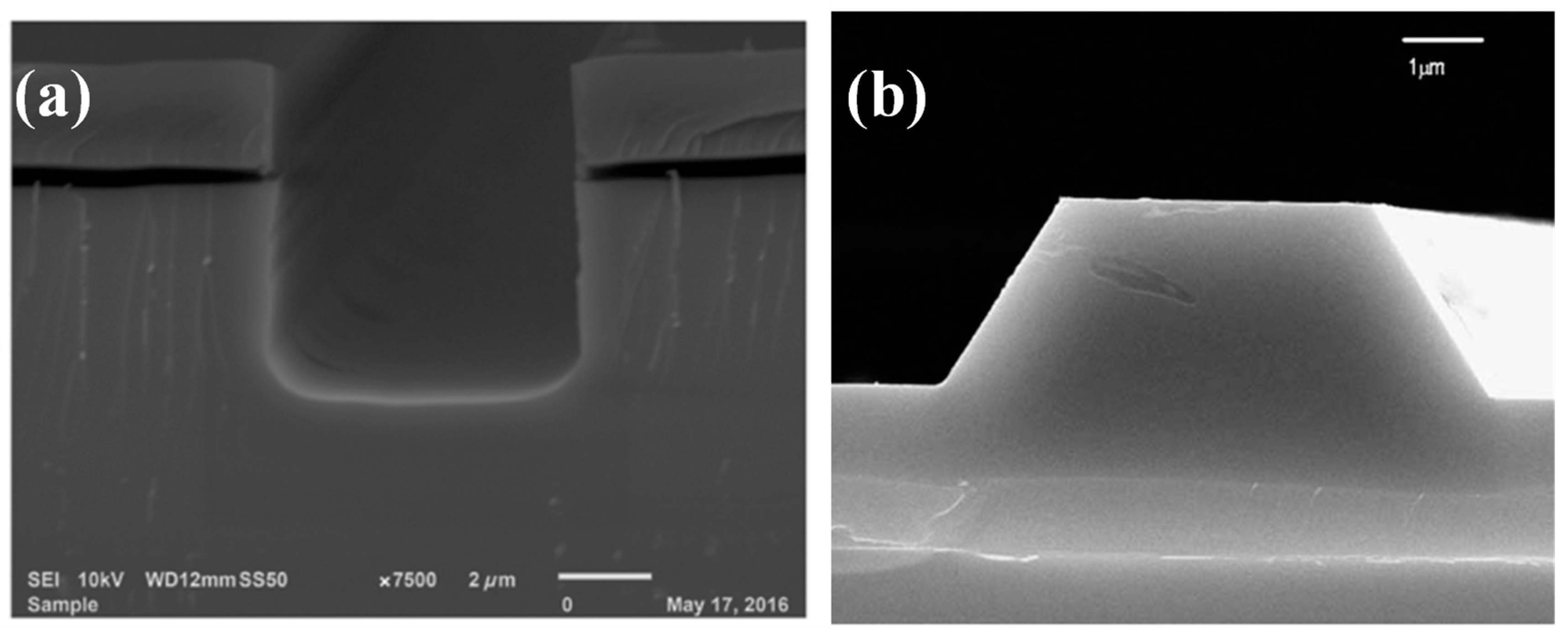
RIE offers higher anisotropy compared to chemical etching, meaning that it etches predominantly in a vertical direction, resulting in more well-defined and precise etch profiles [81]. This process made RIE particularly useful for etching deep and narrow features, such as trenches and high-aspect-ratio structures [82]. To achieve smooth and vertical sidewalls in micropatterned silicon substrates, a low-power etching recipe that utilizes a RIE tool was provided [83]. The employment of CF4, SF6, and O2 gases allowed vertical silicon etching (aspect ratio ~2) at low power (30 W) and low pressure (2 Pa). The etching masks consisted of silicon oxide and photoresist. At a depth of about 4.2 µm, silicon trenches with varying widths and gaps were etched for 40 min. As shown in Figure 5a, a cross-sectional view of trenches that are 4 µm wide and have a 10 µm gap between them allowed the general verticality and smoothness of the walls to be seen. After etching, the remaining 2.3 µm layers of the SU-8 mask, which had a starting thickness of 3.5 µm, were still visible on top of the silicon structures.
4.2. Chemical Etching
Chemical etching is a process that utilizes a chemical solution or etchant to dissolve or etch away material from the substrate [85]. The etchant reacted with the material, breaking down its chemical bonds and removing it in a controlled manner. Chemical etching was typically isotropic, meaning that it uniformly etched in all directions [86]. It was commonly used for etching large-area features, such as wafer-scale patterning, and could be performed at relatively low temperatures. Chemical wet etching could provide high selectivity between different materials using specific etchants that were tailored to each material. Compared to other fabrication techniques, like RIE or laser ablation [87,88], chemical etching could be a cost-effective solution. The equipment and materials required for chemical etching were generally less expensive, making it an attractive option for mass production.
A silica–titanium platform-based reverse rib waveguide (RRWG) structure was subjected to a modal analysis [89]. Both the sol-gel procedure and the dip-coating approach could be used to deposit the silica–titanium WG films. It was suggested that the samples could be structured using chemical wet etching in order to integrate this inexpensive deposition process through a cost-effective production methodology. Wet etching is isotropic; hence, the waveguide layout with rounded sidewalls was thought to best represent the RRWG. Additionally, the RRWG with vertical sidewalls was used to compare the bending loss and modal circumstances [89].
Using a SOI wafer, a 2 × 2 thermo-optic Mach–Zehnder (MZ) switch based on silicon WGs with high cross sections was created [84]. In the MZ structure, the multi-mode interferometers (MMI) served as power combiners and splitters. Anisotropy chemical wet etching of silicon was utilized to create the WGs, rather than dry etching, in order to provide smooth contact. The SEM image of the trapezoidal WG fabricated via KOH chemical wet etching is shown in Figure 5b [84]. Power consumption was decreased by adding more grooves. The gadget features a 235 mW switching power and a 60 µs switching time.
5. Concluding Remarks
Integrated optics refers to the field of study and application of optical components and systems that are integrated onto a single platform or chip. This technology enables the miniaturization, integration, and manipulation of light for various applications. Silicon photonics, polymer photonics, lithium niobate, and indium phosphide photonics are different material platforms used in the field of photonics, which involves the manipulation and transmission of light for various applications. Each of these material platforms has its strengths and weaknesses, and the best choice depends on the specific application requirements. Silicon photonics excels when integrated with electronics, while polymer photonics offers flexibility and low-cost fabrication. Indium phosphide photonics is known for its high-speed and high-frequency capabilities. Researchers and engineers select the most appropriate material platform based on factors such as performance, cost, scalability, and target applications.
Ultra-violet lithography is a widely adopted technique used for high-volume production due to its cost-effective nature and speed. Laser lithography offers improved resolution and flexibility compared to photolithography. Electron beam lithography provides the highest resolution but is generally slower and more expensive, making it suitable for specialized applications and research purposes. Nanoimprint lithography can be a cost-effective alternative to other high-resolution lithography methods, like electron beam lithography. It has the potential for high-throughput production, as it can process large areas of substrates simultaneously. Furthermore, nanoimprint lithography does not require complex and expensive equipment, such as electron beam writers.
Chemical wet etching and reactive ion etching are two commonly used techniques in the fields of microfabrication and semiconductor manufacturing. Both methods are employed to selectively remove material from a substrate to create desired patterns or structures. However, they differ in their mechanisms and characteristics. The choice between chemical wet etching and reactive ion etching depends on several factors, including the desired etch profile, selectivity, material compatibility, throughput, and process complexity. Chemical wet etching is often preferred for carrying out simple and large-area patterning, while reactive ion etching is more suitable for high-resolution and anisotropic etching. The specific requirements of the fabrication process will dictate which technique is more appropriate in each situation. The research is currently focused on the solutions required to create low-cost optical platforms and fabrication methods for the realization of photonic integrated circuits.
Funding
This research received no external funding.
Institutional Review Board Statement
Not applicable.
Informed Consent Statement
Not applicable.
Data Availability Statement
Not applicable.
Acknowledgments
The author acknowledges the support of the Warsaw University of Technology for the completion of this work.
Conflicts of Interest
The author declares no conflict of interest.
Abbreviations
Waveguide = WG; reactive ion etching = RIE; electron beam lithography = EBL; laser lithography = LL; Nanoimprint lithography = NIL; silicon-on-insulator = SOI; radiofrequency = RF; minimum resolvable feature = MRF; ultra-violet lithography = UVL; electromagnetic interference = EMI; photonic integrated circuit = PIC; complementary metal-oxide-semiconductor = CMOS; Indium phosphide = InP; silicon nitride = Si3N4; lithium niobate = LiNbO3.
References
- Eldada, L.; Shacklette, L.W. Advances in polymer integrated optics. IEEE J. Sel. Top. Quantum Electron. 2000, 6, 54–68. [Google Scholar] [CrossRef]
- El-Derhalli, H.; Le Beux, S.; Tahar, S. Stochastic computing with integrated optics. In Proceedings of the 2019 Design, Automation Test in Europe Conference Exhibition, Florence, Italy, 25–29 March 2019; pp. 1355–1360. [Google Scholar]
- Ronggui, S.; Righini, G.C. Characterization of reactive ion etching of glass and its applications in integrated optics. J. Vac. Sci. Technol. A 1991, 9, 2709–2712. [Google Scholar] [CrossRef]
- Khonina, S.N.; Karpeev, S.V.; Butt, M.A. Spatial-Light-Modulator-Based Multichannel Data Transmission by Vortex Beams of Various Orders. Sensors 2021, 21, 2988. [Google Scholar] [CrossRef] [PubMed]
- Kazanskiy, N.L.; Khonina, S.N. Nonparaxial effects in lensacon optical systems. Optoelectron. Instrum. Data Process. 2017, 53, 484–493. [Google Scholar] [CrossRef]
- Dangel, R.; Hofrichter, J.; Horst, F.; Jubin, D.; La Porta, A.; Meier, N.; Soganci, I.M.; Weiss, J.; Offrein, B.J. Polymer waveguides for electro-optical integration in data centers and high-performance computers. Opt. Express 2015, 23, 4736–4750. [Google Scholar] [CrossRef] [PubMed]
- Han, L.; Liang, S.; Xu, J.; Qiao, L.; Zhu, H.; Wang, W. Simultaneous Wavelength- and Mode-Division (De)multiplexing for High-Capacity On-Chip Data Transmission Link. IEEE Photon J. 2016, 8, 1–10. [Google Scholar] [CrossRef]
- Xu, D.; Yan, S.; Yang, X.; Wang, J.; Wu, X.; Hua, E. Tunable Nanosensor With a Horizontal Number Eight-Shape Cavity in a MIM Waveguide System. Front. Phys. 2021, 9, 702193. [Google Scholar] [CrossRef]
- Lu, H.; Wang, G.; Liu, X. Manipulation of light in MIM plasmonic waveguide systems. Chin. Sci. Bull. 2013, 58, 3607–3616. [Google Scholar] [CrossRef] [Green Version]
- Butt, M.A.; Kazanskiy, N.L.; Khonina, S.N. Miniaturized design of a 1 × 2 plasmonic demultiplexer based on metal–insulator-metal waveguide for telecommunication wavelengths. Plasmonics 2023, 18, 635–641. [Google Scholar] [CrossRef]
- Bagheri, A.; Nazari, F.; Moravvej-Farshi, M.K. Tunable Optical Demultiplexer for Dense Wavelength Division Multiplexing Systems Using Graphene–Silicon Microring Resonators. J. Electron. Mater. 2020, 49, 7410–7419. [Google Scholar] [CrossRef]
- Wang, J.; Chen, P.; Chen, S.; Shi, Y.; Dai, D. Improved 8-channel silicon mode demultiplexer with grating polarizers. Opt. Express 2014, 22, 12799–12807. [Google Scholar] [CrossRef] [PubMed]
- Koonen, A.M.J.; Chen, H.; Boom, H.P.A.V.D.; Raz, O. Silicon Photonic Integrated Mode Multiplexer and Demultiplexer. IEEE Photon Technol. Lett. 2012, 24, 1961–1964. [Google Scholar] [CrossRef]
- Khonina, S.N.; Voronkov, G.S.; Grakhova, E.P.; Kazanskiy, N.L.; Kutluyarov, R.V.; Butt, M.A. Polymer Waveguide-Based Optical Sensors—Interest in Bio, Gas, Temperature, and Mechanical Sensing Applications. Coatings 2023, 13, 549. [Google Scholar] [CrossRef]
- Su, Y.; Zhang, Y.; Qiu, C.; Guo, X.; Sun, L. Silicon photonic platform for passive waveguide devices: Materials, fabrication, and applications. Adv. Mater. Technol. 2020, 5, 1901153. [Google Scholar] [CrossRef]
- Yan, Z.; Han, Y.; Lin, L.; Xue, Y.; Ma, C.; Ng, W.K.; Wong, K.S.; Lau, K.M. A monolithic InP/SOI platform for integrated photonics. Light. Sci. Appl. 2021, 10, 1–10. [Google Scholar] [CrossRef]
- Hsu, W.-C.; Zhen, C.; Wang, A.X. Electrically Tunable High-Quality Factor Silicon Microring Resonator Gated by High Mobility Conductive Oxide. ACS Photon 2021, 8, 1933–1936. [Google Scholar] [CrossRef]
- Cohen, R.A.; Amrani, O.; Ruschin, S. Response shaping with a silicon ring resonator via double injection. Nat. Photon 2018, 12, 706–712. [Google Scholar] [CrossRef]
- Koala, R.A.S.D.; Fujita, M.; Nagatsuma, T. Nanophotonics-inspired all-silicon waveguide platforms for terahertz integrated systems. Nanophotonics 2022, 11, 1741–1759. [Google Scholar] [CrossRef]
- Tan, Y.; Dai, D. Silicon microring resonators. J. Opt. 2018, 20, 054004. [Google Scholar] [CrossRef]
- Liao, J.; Tian, Y.; Yang, Z.; Zhang, X. Inverse design of optical couplers with arbitrary splitting ratio based on boundary inverse optimization algorithm. Acta Opt. Sin. 2023, 43, 0113001. [Google Scholar]
- Ding, R.; Baehr-Jones, T.; Kim, W.-J.; Xiong, X.; Bojko, R.; Fedeli, J.-M.; Fournier, M.; Hochberg, M. Low-loss strip-loaded slot waveguides in Silicon-on-Insulator. Opt. Express 2010, 18, 25061–25067. [Google Scholar] [CrossRef]
- Ishutkin, S.; Arykov, V.; Yunusov, I.; Stepanenko, M.; Smirnov, V.; Troyan, P.; Zhidik, Y. The Method of Low-Temperature ICP Etching of InP/InGaAsP Heterostructures in Cl2-Based Plasma for Integrated Optics Applications. Micromachines 2021, 12, 1535. [Google Scholar] [CrossRef]
- Vivien, L.; Marris-Morini, D.; Griol, A.; Gylfason, K.B.; Hill, D.; Alvarez, J.; Sohlström, H.; Hurtado, J.; Bouville, D.; Cassan, E. Vertical multiple-slot waveguide ring resonators in silicon nitride. Opt. Express 2008, 16, 17237–17242. [Google Scholar] [CrossRef] [PubMed] [Green Version]
- Krasnokutska, I.; Tambasco, J.-L.J.; Li, X.; Peruzzo, A. Ultra-low loss photonic circuits in lithium niobate on insulator. Opt. Express 2018, 26, 897–904. [Google Scholar] [CrossRef] [PubMed] [Green Version]
- Ahmadi, L.; Hiltunen, M.; Stenberg, P.; Hiltunen, J.; Aikio, S.; Roussey, M.; Saarinen, J.; Honkanen, S. Hybrid layered polymer slot waveguide Young interferometer. Opt. Express 2016, 24, 10275–10285. [Google Scholar] [CrossRef]
- Melchior, H. Indium Phosphide Photonic Waveguide Devices and their Fiber Pigtailing. In Integrated Photonics Research; Optica Publishing Group: Washington, DC, USA, 1998; p. IMA2. [Google Scholar]
- Moss, D.J.; Morandotti, R.; Gaeta, A.L.; Lipson, M. New CMOS-compatible platforms based on silicon nitride and Hydex for nonlinear optics. Nat. Photonics 2013, 7, 597–607. [Google Scholar] [CrossRef] [Green Version]
- Chia, X.X.; Tan, D.T.H. Deuterated SiNx: A low-loss, back-end CMOS-compatible platform for nonlinear integrated optics. Nanophotonics 2023, 12, 1613–1631. [Google Scholar] [CrossRef]
- Alexander, K.; George, J.P.; Verbist, J.; Neyts, K.; Kuyken, B.; Van Thourhout, D.; Beeckman, J. Nanophotonic Pockels modulators on a silicon nitride platform. Nat. Commun. 2018, 9, 3444. [Google Scholar] [CrossRef] [Green Version]
- Bhandari, B.; Im, C.-S.; Sapkota, O.R.; Lee, S.-S. Highly efficient broadband silicon nitride polarization beam splitter incorporating serially cascaded asymmetric directional couplers. Opt. Lett. 2020, 45, 5974–5977. [Google Scholar] [CrossRef]
- Antonacci, G.; Elsayad, K.; Polli, D. On-Chip Notch Filter on a Silicon Nitride Ring Resonator for Brillouin Spectroscopy. ACS Photon 2022, 9, 772–777. [Google Scholar] [CrossRef]
- Han, Q.; St-Yves, J.; Chen, Y.; Ménard, M.; Shi, W. Polarization-insensitive silicon nitride arrayed waveguide grating. Opt. Lett. 2019, 44, 3976–3979. [Google Scholar] [CrossRef] [PubMed]
- Kumar, M.; Muniswamy, V.; Guha, K.; Iannacci, J.; Krishnaswamy, N. Analysis of integrated silicon nitride lab-on-a-chip optofluidic sensor at visible wavelength for absorbance based biosensing applications. Microsyst. Technol. 2021, 27, 3499–3506. [Google Scholar] [CrossRef]
- Wang, L.; Xie, W.; Van Thourhout, D.; Zhang, Y.; Yu, H.; Wang, S.H. Nonlinear silicon nitride waveguides based on PECVD deposition platform. Opt. Express 2018, 26, 9645–9654. [Google Scholar] [CrossRef] [Green Version]
- Senichev, A.; Peana, S.; Martin, Z.O.; Yesilyurt, O.; Sychev, D.; Lagutchev, A.S.; Boltasseva, A.; Shalaev, V.M. Silicon Nitride Waveguides with Intrinsic Single-Photon Emitters for Integrated Quantum Photonics. ACS Photon 2022, 9, 3357–3365. [Google Scholar] [CrossRef]
- DSun, D.; Zhang, Y.; Wang, D.; Song, W.; Liu, X.; Pang, J.; Geng, D.; Sang, Y.; Liu, H. Microstructure and domain engineering of lithium niobate crystal films for integrated photonic applications. Light. Sci. Appl. 2020, 9, 197. [Google Scholar] [CrossRef]
- Kotlyar, M.V.; Iadanza, S.; O’faolain, L. Lithium Niobate Fabry-Perot microcavity based on strip loaded waveguides. Photon Nanostructures—Fundam. Appl. 2021, 43, 100886. [Google Scholar] [CrossRef]
- Carletti, L.; Li, C.; Sautter, J.; Staude, I.; De Angelis, C.; Li, T.; Neshev, D.N. Second harmonic generation in monolithic lithium niobate metasurfaces. Opt. Express 2019, 27, 33391–33398. [Google Scholar] [CrossRef]
- Li, M.; Ling, J.; He, Y.; Javid, U.A.; Xue, S.; Lin, Q. Lithium niobate photonic-crystal electro-optic modulator. Nat. Commun. 2020, 11, 4123. [Google Scholar] [CrossRef]
- Saravi, S.; Pertsch, T.; Setzpfandt, F. Lithium Niobate on Insulator: An Emerging Platform for Integrated Quantum Photonics. Adv. Opt. Mater. 2021, 9, 2100789. [Google Scholar] [CrossRef]
- Han, X.-Y.; Wu, Z.-L.; Yang, S.-C.; Shen, F.-F.; Liang, Y.-X.; Wang, L.-H.; Wang, J.-Y.; Ren, J.; Jia, L.-Y.; Zhang, H.; et al. Recent Progress of Imprinted Polymer Photonic Waveguide Devices and Applications. Polymers 2018, 10, 603. [Google Scholar] [CrossRef] [Green Version]
- Zhou, J.; Wong, W.H.; Pun, E.Y.B.; Shen, Y.Q.; Zhao, Y.X. Fabrication of low loss optical waveguides with a novel thermo-optical polymer material. Opt. Appl. 2006, 36, 429. [Google Scholar]
- Eldada, L.; Blomquist, R.; Maxfield, M.; Pant, D.; Boudoughian, G.; Poga, C.; Norwood, R. Thermooptic planar polymer Bragg grating OADMs with broad tuning range. IEEE Photon Technol. Lett. 1999, 11, 448–450. [Google Scholar] [CrossRef]
- Kazanskiy, N.L.; Butt, M.A.; Khonina, S.N. Carbon Dioxide Gas Sensor Based on Polyhexamethylene Biguanide Polymer Deposited on Silicon Nano-Cylinders Metasurface. Sensors 2021, 21, 378. [Google Scholar] [CrossRef]
- Kagami, M.; Kawasaki, A.; Ito, H. A polymer optical waveguide with out-of-plane branching mirrors for surface-normal optical interconnections. J. Light. Technol. 2001, 19, 1949–1955. [Google Scholar] [CrossRef]
- Halldorsson, J.; Arnfinnsdottir, N.B.; Jonsdottir, A.B.; Agnarsson, B.; Leosson, K. High index contrast polymer waveguide platform for integrated biophotonics. Opt. Express 2010, 18, 16217–16226. [Google Scholar] [CrossRef]
- Oh, D.J.; Jung, J.H.; Kang, J.Y.; Lee, S.H. A disposable polymer waveguide lab-on-a-chip for real-time detection of protein c using evanescent wave. In Proceedings of the SENSORS, 2010 IEEE, Waikoloa, HI, USA, 1–4 November 2010; pp. 1605–1608. [Google Scholar]
- Kazanskiy, N.L.; Butt, M.A.; Khonina, S.N. Recent Advances in Wearable Optical Sensor Automation Powered by Battery versus Skin-like Battery-Free Devices for Personal Healthcare—A Review. Nanomaterials 2022, 12, 334. [Google Scholar] [CrossRef]
- Butt, M.A.; Kazanskiy, N.L.; Khonina, S.N. Advances in Waveguide Bragg Grating Structures, Platforms, and Applications: An Up-to-Date Appraisal. Biosensors 2022, 12, 497. [Google Scholar] [CrossRef]
- Sharma, E.; Rathi, R.; Misharwal, J.; Sinhmar, B.; Kumari, S.; Dalal, J.; Kumar, A. Evolution in Lithography Techniques: Microlithography to Nanolithography. Nanomaterials 2022, 12, 2754. [Google Scholar] [CrossRef]
- Huang, Y.; Zhao, Q.; Kamyab, L.; Rostami, A.; Capolino, F.; Boyraz, O. Sub-micron silicon nitride waveguide fabrication using conventional optical lithography. Opt. Express 2015, 23, 6780–6786. [Google Scholar] [CrossRef] [Green Version]
- Bednorz, M.; Urbańczyk, M.; Pustelny, T.; Piotrowska, A.; Papis, E.; Sidor, Z.; Kamińska, E. Application of SU8 polymer in waveguide interferometer ammonia sensor. Mol. Quantum Acoust. 2006, 27, 31–40. [Google Scholar]
- Wen, X.; Datta, A.; Traverso, L.M.; Pan, L.; Xu, X.; Moon, E.E. High throughput optical lithography by scanning a massive array of bowtie aperture antennas at near-field. Sci. Rep. 2015, 5, 16192. [Google Scholar] [CrossRef] [PubMed] [Green Version]
- Okazaki, S. High resolution optical lithography or high throughput electron beam lithography: The technical struggle from the micro to the nano-fabrication evolution. Microelectron. Eng. 2015, 133, 23–35. [Google Scholar] [CrossRef]
- Ocier, C.R.; Richards, C.A.; Bacon-Brown, D.A.; Ding, Q.; Kumar, R.; Garcia, T.J.; van de Groep, J.; Song, J.-H.; Cyphersmith, A.J.; Rhode, A.; et al. Direct laser writing of volumetric gradient index lenses and waveguides. Light. Sci. Appl. 2020, 9, 1–14. [Google Scholar] [CrossRef] [PubMed]
- Lü, L.; Fuh, J.Y.H.; Wong, Y.S.; Lü, L.; Fuh, J.Y.H.; Wong, Y.S. Fundamentals of laser-lithography processes. In Laser-Induced Materials and Processes for Rapid Prototyping; Springer: Boston, MA, USA, 2001; pp. 9–38. [Google Scholar]
- Patolyatov, A.D.; Shcherbakov, D.A.; Kolymagin, D.A.; Matital, R.P.; Chubich, D.A.; Vitukhovsky, A.G. Erratum to: Refractive X-Ray Lenses Made by the Two-Photon Laser Lithography Method. Phys. Wave Phenom. 2022, 30, 401. [Google Scholar] [CrossRef]
- Bogaerts, W.; Wiaux, V.; Taillaert, D.; Beckx, S.; Luyssaert, B.; Bienstman, P.; Baets, R. Fabrication of photonic crystals in silicon-on-insulator using 248-nm deep UV lithography. IEEE J. Sel. Top. Quantum Electron. 2002, 8, 928–934. [Google Scholar] [CrossRef] [Green Version]
- Broers, A.N. Resolution limits for electron-beam lithography. IBM J. Res. Dev. 1988, 32, 502–513. [Google Scholar] [CrossRef]
- Broers, A.N.; Hoole, A.C.F.; Ryan, J.M. Electron beam lithography—Resolution limits. Microelectron. Eng. 1996, 32, 131–142. [Google Scholar] [CrossRef]
- Eissa, M.; Mitarai, T.; Amemiya, T.; Miyamoto, Y.; Nishiyama, N. Fabrication of Si photonic waveguides by electron beam lithography using improved proximity effect correction. Jpn. J. Appl. Phys. 2020, 59, 126502. [Google Scholar] [CrossRef]
- Zheng, Y.; Gao, P.-P.; Tang, X.; Liu, J.-Z.; Duan, J.-A. Effects of electron beam lithography process parameters on structure of silicon optical waveguide based on SOI. J. Central South Univ. 2022, 29, 3335–3345. [Google Scholar] [CrossRef]
- Geka, G.; Papageorgiou, G.; Chatzichristidi, M.; Karydas, A.G.; Psycharis, V.; Makarona, E. CuO/PMMA Polymer Nanocomposites as Novel Resist Materials for E-Beam Lithography. Nanomaterials 2021, 11, 762. [Google Scholar] [CrossRef]
- Tu, M.; Xia, B.; Kravchenko, D.E.; Tietze, M.L.; Cruz, A.J.; Stassen, I.; Hauffman, T.; Teyssandier, J.; De Feyter, S.; Wang, Z.; et al. Direct X-ray and electron-beam lithography of halogenated zeolitic imidazolate frameworks. Nat. Mater. 2020, 20, 93–99. [Google Scholar] [CrossRef] [PubMed]
- Dey, R.K.; Cui, B. Stitching error reduction in electron beam lithography with in-situ feedback using self-developing resist. J. Vac. Sci. Technol. B 2013, 31, 06F409. [Google Scholar] [CrossRef] [Green Version]
- Choi, K.-H.; Huh, J.; Cui, Y.; Trivedi, K.; Hu, W.; Ju, B.-K.; Lee, J.-B. One-Step Combined-Nanolithography-and-Photolithography for a 2D Photonic Crystal TM Polarizer. Micromachines 2014, 5, 228–238. [Google Scholar] [CrossRef] [Green Version]
- Yun, B.; Hu, G.; Cui, Y. Third-order polymer waveguide Bragg grating array by using conventional contact lithography. Opt. Commun. 2014, 330, 113–116. [Google Scholar] [CrossRef]
- Bogdanov, A.L.; Lapointe, J.; Schmid, J.H. Electron-beam lithography for photonic waveguide fabrication: Measurement of the effect of field stitching errors on optical performance and evaluation of a new compensation method. J. Vac. Sci. Technol. B 2012, 30, 031606. [Google Scholar] [CrossRef]
- Wang, Z.; Gui, L.; Han, D.; Xu, Z.; Han, L.; Xu, S. Measurement and Evaluation of Local Surface Temperature Induced by Irradiation of Nanoscaled or Microscaled Electron Beams. Nanoscale Res. Lett. 2019, 14, 1–11. [Google Scholar] [CrossRef] [Green Version]
- Butt, M.A. Thin-Film Coating Methods: A Successful Marriage of High-Quality and Cost-Effectiveness—A Brief Exploration. Coatings 2022, 12, 1115. [Google Scholar] [CrossRef]
- Grego, S.; Huffman, A.; Lueck, M.; Stoner, B.R.; Lannon, J. Nanoimprint lithography fabrication of waveguide-integrated optical gratings with inexpensive stamps. Microelectron. Eng. 2010, 87, 1846–1851. [Google Scholar] [CrossRef]
- Prajzler, V.; Chlupaty, V.; Kulha, P.; Neruda, M.; Kopp, S.; Mühlberger, M. Optical Polymer Waveguides Fabricated by Roll-to-Plate Nanoimprinting Technique. Nanomaterials 2021, 11, 724. [Google Scholar] [CrossRef]
- Bruinink, C.M.; Burresi, M.; de Boer, M.J.; Segerink, F.B.; Jansen, H.V.; Berenschot, E.; Reinhoudt, D.N.; Huskens, J.; Kuipers, L. Nanoimprint Lithography for Nanophotonics in Silicon. Nano Lett. 2008, 8, 2872–2877. [Google Scholar] [CrossRef]
- Shneidman, A.V.; Becker, K.P.; Lukas, M.A.; Torgerson, N.; Wang, C.; Reshef, O.; Burek, M.J.; Paul, K.; McLellan, J.; Lončar, M. All-Polymer Integrated Optical Resonators by Roll-to-Roll Nanoimprint Lithography. ACS Photon 2018, 5, 1839–1845. [Google Scholar] [CrossRef]
- Gao, F.; Ylinen, S.; Kainlauri, M.; Kapulainen, M. Smooth silicon sidewall etching for waveguide structures using a modified Bosch process. J. Micro/Nanolithography MEMS MOEMS 2014, 13, 13010. [Google Scholar] [CrossRef]
- Zheng, Y.; Gao, P.; Jiang, L.; Kai, X.; Duan, J. Surface Morphology of Silicon Waveguide after Reactive Ion Etching (RIE). Coatings 2019, 9, 478. [Google Scholar] [CrossRef] [Green Version]
- Hiscocks, M.P.; Ganesan, K.; Gibson, B.C.; Huntington, S.T.; Ladouceur, F.; Prawer, S. Diamond waveguides fabricated by reactive ion etching. Opt. Express 2016, 16, 19512–19519. [Google Scholar] [CrossRef] [PubMed]
- Kozlov, A.; Moskalev, D.; Salgaeva, U.; Bulatova, A.; Krishtop, V.; Volyntsev, A.; Syuy, A. Reactive Ion Etching of X-Cut LiNbO3 in an ICP/TCP System for the Fabrication of an Optical Ridge Waveguide. Appl. Sci. 2023, 13, 2097. [Google Scholar] [CrossRef]
- Kim, T.; Lee, J. Optimization of deep reactive ion etching for microscale silicon hole arrays with high aspect ratio. Micro Nano Syst. Lett. 2022, 10, 1–7. [Google Scholar] [CrossRef]
- Li, W.; Luo, Y.; Xiong, B.; Sun, C.; Wang, L.; Wang, J.; Lu, H. Fabrication of GaN-based ridge waveguides with very smooth and vertical sidewalls by combined plasma dry etching and wet chemical etching. Phys. Status Solidi 2015, 212, 2341–2344. [Google Scholar] [CrossRef]
- Liao, Z.; Aitchison, J.S. Precision etching for multi-level AlGaAs waveguides. Opt. Mater. Express 2017, 7, 895–903. [Google Scholar] [CrossRef]
- Ashraf, M.; Sundararajan, S.V.; Grenci, G. Low-power, low-pressure reactive-ion etching process for silicon etching with vertical and smooth walls for mechanobiology application. J. Micro/Nanolithography, MEMS, MOEMS 2017, 16, 34501. [Google Scholar] [CrossRef] [Green Version]
- Xia, J.; Yu, J.; Wang, Z.; Fan, Z.; Chen, S. Low power 2 × 2 thermo-optic SOI waveguide switch fabricated by anisotropy chemical etching. Opt. Commun. 2004, 232, 223–228. [Google Scholar] [CrossRef]
- Chuang, M.J.; Hsieh, K.Y.; Chu, A.K. High-Temperature Wet Chemical Etching of Ta2 O 5 in NaOH-Based Solutions for Fabricating Antiresonant Reflecting Optical Waveguides. J. Electrochem. Soc. 1998, 145, 1020. [Google Scholar] [CrossRef]
- Bauhuber, M.; Mikrievskij, A.; Lechner, A. Isotropic wet chemical etching of deep channels with optical surface quality in silicon with HNA based etching solutions. Mater. Sci. Semicond. Process. 2013, 16, 1428–1433. [Google Scholar] [CrossRef]
- Jelinek, M.; Lančok, J.; Sonsky, J.; Oswald, J.; Šimečková, M.; Jastrabik, L.; Studnička, V.; Grivas, C.; Hříbek, P. Planar waveguide lasers and structures created by laser ablation—An overview. Czechoslov. J. Phys. 1998, 48, 577–597. [Google Scholar] [CrossRef]
- Kam, W.; Ong, Y.; Lim, W.; Zakaria, R. Laser ablation and waveguide fabrication using CR39 polymer. Opt. Lasers Eng. 2014, 55, 1–4. [Google Scholar] [CrossRef]
- Butt, M.A.; Kozlowski, L.; Piramidowicz, R. Numerical scrutiny of a silica-titania-based reverse rib waveguide with vertical and rounded sidewalls. Appl. Opt. 2023, 62, 1296–1302. [Google Scholar] [CrossRef] [PubMed]
Figure 1.
Optical platforms studied in this work.

Figure 2.
(a) Optical micrograph image of a group of strip-loaded slot WG runouts of different lengths, adapted from [22]; (b) SEM image showing the stack of WG, buried oxide layer, and silicon substrate, adapted from [22], (c) SEM micrograph of the ridge WG to strip-loaded slot WG transition region, adapted from [22]; (d) SEM images of the WG structure formed in the p-i-n InP/InGaAsP heterostructure, adapted from [23]; (e) SEM image of the ring resonator structure based on multiple slot WGs, adapted from [24]; (f) ring resonator structure based on the LNOI platform, adapted from [25]; and (g) the SEM image of the Y-junction on polymer WG, adapted from [26].

Figure 3.
The types of lithography methods debated in this entry.

Figure 4.
Most widely used fabrication methods in research and commercial applications.


Disclaimer/Publisher’s Note: The statements, opinions and data contained in all publications are solely those of the individual author(s) and contributor(s) and not of MDPI and/or the editor(s). MDPI and/or the editor(s) disclaim responsibility for any injury to people or property resulting from any ideas, methods, instructions or products referred to in the content. |
© 2023 by the author. Licensee MDPI, Basel, Switzerland. This article is an open access article distributed under the terms and conditions of the Creative Commons Attribution (CC BY) license (https://creativecommons.org/licenses/by/4.0/).
Share and Cite
MDPI and ACS Style
Butt, M.A. Integrated Optics: Platforms and Fabrication Methods. Encyclopedia 2023, 3, 824-838. https://doi.org/10.3390/encyclopedia3030059
AMA Style
Butt MA. Integrated Optics: Platforms and Fabrication Methods. Encyclopedia. 2023; 3(3):824-838. https://doi.org/10.3390/encyclopedia3030059
Chicago/Turabian StyleButt, Muhammad A. 2023. "Integrated Optics: Platforms and Fabrication Methods" Encyclopedia 3, no. 3: 824-838. https://doi.org/10.3390/encyclopedia3030059