Article

A 10 V Transfer Standard Based on Low-Noise Solid-State Zener Voltage Reference ADR1000

1
Hahn-Schickard, Allmandring 9b, 70569 Stuttgart, Germany
2
Institute for Micro Integration (IFM), University of Stuttgart, Allmandring 9b, 70569 Stuttgart, Germany
*
Author to whom correspondence should be addressed.
Metrology 2024, 4(1), 98-116; https://doi.org/10.3390/metrology4010007
Submission received: 20 December 2023 / Revised: 14 February 2024 / Accepted: 26 February 2024 / Published: 5 March 2024

Abstract

:
Voltage standards are widely used to transfer volts from Josephson voltage standards (JVSs) at national metrology institutes (NMIs) into calibration labs to maintain the volts and to transfer them to test equipment at production lines. Therefore, commercial voltage standards based on Zener diodes are used. Analog Devices Inc. (San Jose, CA, USA), namely, Eric Modica, introduced the ADR1000KHZ, a successor to the legendary LTZ1000, at the Metrology Meeting 2021. The first production samples were already available prior to this event. In this article, this new temperature-stabilized Zener diode is compared to several others as per datasheet specifications. Motivated by the superior parameters, a 10 V transfer standard prototype for laboratory use with commercial off-the-shelf components such as resistor networks and chopper amplifiers was built. How much effort it takes to reach the given parameters was investigated. This paper describes how the reference was set up to operate it at its zero-temperature coefficient (z.t.c.) temperature and to lower the requirements for the oven stability. Furthermore, it is shown how the overall temperature coefficient (t.c.) of the circuit was reduced. For the buffered Zener voltage, a t.c. of almost zero, and with amplification to 10 V, a t.c. of <0.01 µV/V/K was achieved in a temperature span of 15 to 31 °C. For the buffered Zener voltage, a noise of ~584 nVp-p and for the 10 V output, ~805 nVp-p were obtained. Finally, 850 days of drift data were taken by comparing the transfer standard prototype to two Fluke 7000 voltage standards according to the method described in NBS Technical Note 430. The drift specification was, however, not met.

1. Introduction

Zener diodes as voltage references are used in test equipment such as digital multimeters (DMM), calibrators, voltage, and transfer standards. They still outperform bandgap references in terms of temperature coefficient (t.c.), noise, and long-term stability, which to some extent is achieved by temperature compensation with a forward-biased silicon diode or transistor wired as a diode and/or temperature stabilization, larger reference voltages, and process improvements such as the invention of the buried Zener diode.
In DMMs, the voltage reference serves as a counterweight to an unknown voltage at its input, while the DMM itself acts as a balance. In calibrators, it is the source from which a programmable output voltage is derived. In voltage standards, they are used to maintain and as a transfer standard to import or exchange the voltage between two consequent calibrations at national metrology institutes (NMIs) or other calibration labs. The next to last has the highest demand on t.c., noise, and long-term stability. Since their invention, voltage references have detached galvanic cells such as unsaturated as well as saturated cells, like Clark and Weston cells. The Weston cell defined the voltage in the SI (International System of Units) until it was superseded by the Josephson voltage standard (JVS) in 1990. The first legal standard for the volt, namely, the Clark cell, was defined in 1894 by the U.S. Congress. The first standards were based on chemical cells. The Clark cell was already superseded by the Weston cell in 1908 at the London International Conference on Electrical Units and Standards. From there on, Weston cells were the new standard for the volt, as they showed many advantages over Clark cells. Nevertheless, these cells are sensitive to transport, changes in temperature, and small electrical currents. To maintain long-term stability, a group of cells was used as a standard to compare the cells among each other and replace cells when necessary [1]. Since 1948, the National Reference Group of Standard Cells has consisted of 44 saturated Weston cells that were made from highly purified materials and assembled under controlled conditions [1,2].
In the early 1960s, a new voltage reference appeared due to the growing semiconductor industry. The solid-state Zener diode started to replace standard chemical cells for commercial use, though they exhibited higher noise compared to standard cells. Further drawbacks were their sensitivity to temperature, atmospheric pressure, and relative humidity. Their overall advantage was the possibility for robust transportation [1].
In 1962, Brian Josephson predicted the Josephson effect, which was confirmed by experiments one year later. He predicted that if an alternating current of frequency f is driven through superconductor materials that are separated by a thin non-conducting material, a tunnel effect occurs [3]. The generated voltage Vn is defined by
V n = n h f 2 e ,
where n is an integer value, h is Planck’s constant, and e is the elementary charge. The ratio 2 e h 483.6   M H z / µ V is defined as the Josephson constant [1,3]. In the beginning, only small voltages could be generated, which made it necessary to scale the values by a factor of 100 and led to limitations until, in 1977, it was discovered that irradiation with microwaves leads to quantized DC voltages in unbiased Josephson junctions. This was the start of Josephson junction arrays in combination with radio frequency fields to generate several volts [3]. To be in the range of one volt and above, several thousands of junctions are necessary [1,3]. On 1 January 1990, the Josephson constant became the new U.S. legal volt [1] and the JVS became the standard in NMIs. Further derivatives of JVS are programmable Josephson voltage standards (PJVSs), which can be used to set the number of junctions and generate a desired voltage with high accuracy [3], as well as Josephson arbitrary waveform synthesizers (JAWSs). However, the operation of a JVS is rather expensive, as it only works at cryo-temperatures and requires liquid helium, has complex and high-cost components, and is of large size. In this regard, there is some effort to setup JVSs that are more compact in order to use them in calibration labs [4].
Meanwhile, a bank of Zener diode-based voltage standards is used as of today to maintain the volt and to transfer it to calibration labs, while the bank is calibrated to the JVS on a regular basis at NMIs. Table 1 lists commercial voltage standards. It includes the reference ICs used in the standard, stability of the system in a given period of time, t.c., noise, and whether the system uses an oven. The values provided in Table 1 give a hint about the comparability of the standards, because the values are provided in different units if available at all. Besides information from datasheets that do not always contain complete specifications, few scientific papers have focused on the specification of Zener-based voltage standards regarding noise, t.c., stability, and other characteristics. There has not been much research conducted recently in this field, and many standards have existed for several decades with no successor. There are, however, a few publications on this topic from the last decades that will shortly be introduced. The entries of ADCMT 6900 for stability and t.c. in Table 1 are the experimental results in [5]. Further research on this standard dealt with the influence of atmospheric pressure on the standard [6]. Ref. [7] investigated the behavior of voltage standards with Zener-based voltage references in a test scenario with power interruptions and their resulting drift. Ref. [8] presents a prototype 10 V standard based on LTZ1000 with details on the electrical circuit and relevant components to adjust temperature and voltage in combination with resistor standards. Ref. [9] proposes mathematical models for the long- and medium-term drift of voltage standards as well as measurements on four different commercial standards, namely, Fluke 732A, Fluke 732B, Datron 4910, and Guildline 4410. Measurement values were taken in an annual comparison over a period of 10 years. The column reference IC in Table 1 includes the Zener diode used in these particular standards. In the simplest version, this is a combination of a Zener diode and a forward-biased diode or a combination of a Zener diode and a bipolar transistor. Some of them include an on-chip heater, additional temperature sensors, or complete oven controllers.
Zener diodes are driven in reverse direction. At small reverse voltages, the current is mainly blocked, whereas at higher reverse voltages, the avalanche effect occurs. In avalanche mode, the current I Z increases rapidly, with only small changes in voltage V Z . The capability of a Zener diode to regulate a voltage is measured by its dynamic impedance as Z Z = V Z I Z at a given operating current [21]. As mentioned before, Zener diodes are temperature dependent. Typically, they have a positive t.c. For this reason, a forward-biased silicon diode, which has a negative t.c., is used in series with it. For a specific operating current, these diodes in combination provide a near-zero temperature coefficient (z.t.c.) [22]. A popular reference diode of this type is the 1N829. Besides this simplest type of voltage reference, there are types including a bipolar transistor instead of a diode. Examples of this type are DH80417B, SZA263, and later, LTFLU. Only little is known about them because they were or are exclusively manufactured for Fluke. Hence, no official datasheets are available. The LTFLU is, however, the successor for the SZA263, which was manufactured by Motorola and used in Fluke 731A/B, 732A (Table 1), which again is the successor of the DH80417B, manufactured by multiple companies, such as Dickson, Siemens & Halske, as well as Texas Instruments. Those three voltage references are often called refamps. Although the LTFLU is a refamp on a single die containing four buried Zener diodes (BZD) in parallel [23,24], SZA263 and earlier DH80417B contained two dies, a Zener diode and a transistor [23,25]. All three of them are unheated devices, although LTFLU seems to contain two unused heater resistors [26]. This is why the LTFLU in Fluke 732A/B/C is located inside a discrete oven assembly together with hermetically sealed resistors or custom resistor networks and associated operational amplifiers. Multiple publications report superior long-term behavior for such voltage standards [27,28,29].
To obtain even better performance in noise and stability, sub-surface Zener diodes were invented, also referred to as BZDs. Further developments of voltage references led to temperature-stabilized BZDs like LMx99. In addition to a BZD and a bipolar transistor, they include a temperature sensor and a heater control circuit to stabilize the reference diode at a certain temperature. As an example, LMx99 is a precision, temperature-stabilized subsurface or buried Zener reference with the oven operating at a fixed temperature of ~90 °C and is a reference that was invented at National Semiconductor and later also fabricated by Linear Technology. Eventually, the Ultra-Zener LTZ1000 was invented, which includes a BZD, a heater, and a temperature-sensing transistor [30]. Here, the Zener current and oven temperature can be set individually by external components for a specific target application. For about 35 years, it was the state-of-the-art commercially available high-precision voltage reference without any successor. Table 2 lists the most important parameters of all commercially available voltage references used in voltage standards for comparison.
At the Metrology Meeting 2021 in Stuttgart, Germany, Eric Modica, design manager in the precision converter group at Analog Devices Inc. (San Jose, CA, USA) and project manager to second source the LTZ1000, introduced a few new temperature-stabilized, Zener-based voltage references to the broad community in a public talk, that is, ADR1399 as a successor to the LMx99 and ADR1000KHZ as a successor to the LTZ1000. In prospect, he also introduced ADR1001, which could be understood as a single-chip solution to create either 5 V or 10 V, with additional OpAmps and associated resistors in one package. All of the mentioned references are BZDs. The development started in 2016, when ADI began an internal project to second source the LTZ1000 for their converter products.
From a user point of view, the ADR1399 is similar but has lower noise and is a lower t.c. drop-in replacement for the LMx99 with the oven operating at ~95 °C. The ADR1000, however, is somewhat similar to the LTZ1000 but features lower noise, as provided in Table 2.
Motivated by the superior parameters, a 10 V transfer standard prototype for laboratory use with commercial off-the-shelf components such as resistor networks and chopper amplifiers was built to investigate how much effort it takes to reach the parameters provided in the datasheet of the voltage reference.

2. Materials and Methods

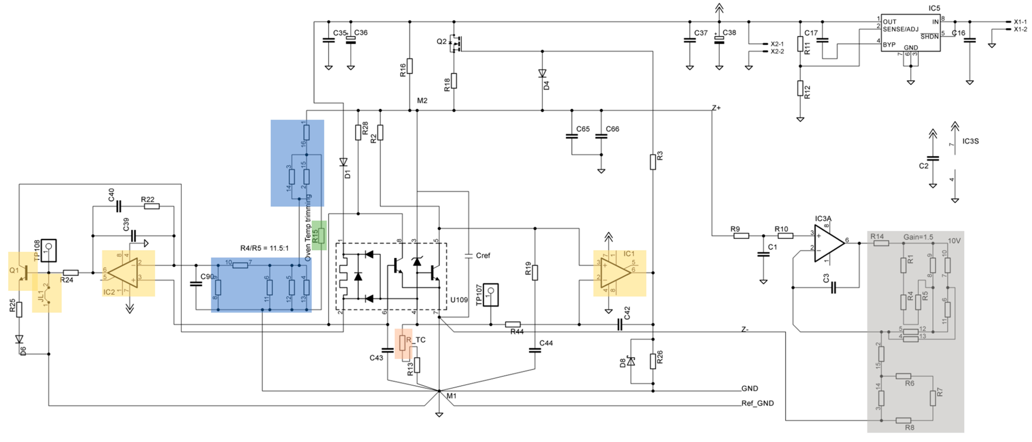
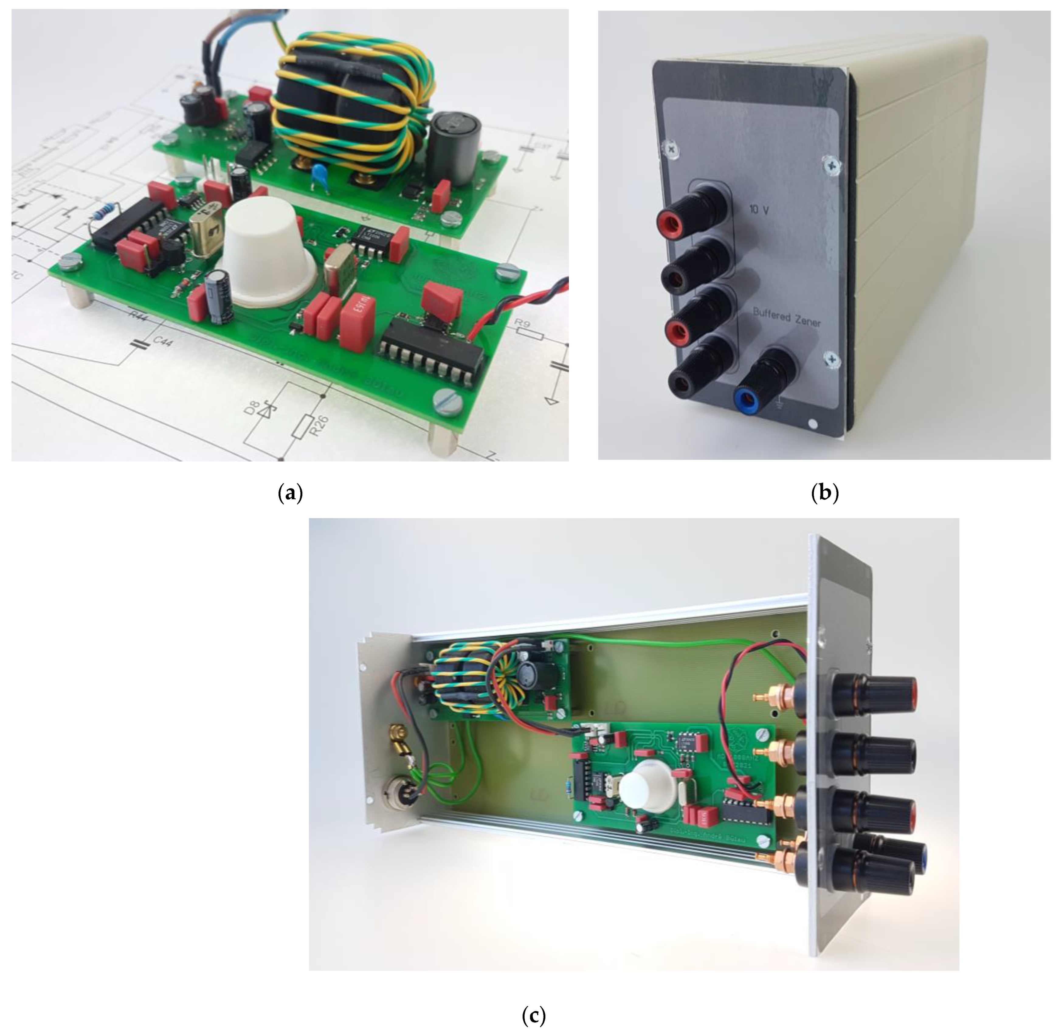
2.1. Design of the Reference

The schematic for the transfer standard prototype is provided in Figure 1. Differing from the example in [36], the reference internal heater is connected between the positive supply rail and the collector of Q1. This allows the heater to be turned off by simply tying the base of the transistor to the ground, which is achieved with jumper JL1. Similar to [37], the internal temperature-sensing transistor of the reference is used as a diode. Based on the results in [38], resistor networks exhibiting low-frequency noise were chosen for the oven setpoint R4/R5 as well as for the 10 V gain stage. The gain stage uses the low-noise chopper operational amplifier AD4522, while the operational amplifiers related to the heater and bootstrapped Zener are of type LT1006. An LDO type LT1763 provides 12 V to the whole circuit, leading to a large voltage from about 13 V up to 20 V at its input.
The assembled reference board is shown in Figure 2a together with the prospective power supply board in the background, which is basically a copy of the LT1533-based DC-DC converter used in F7000. The assembled 10 V transfer standard in its final enclosure is shown in Figure 2b. The ADR1000 voltage reference is covered on both sides of the board with a wind shield to prevent air drafts. A Fischer Elektronik 19” die-cast aluminum slide-in cassette and low thermal e.m.f. binding posts TBP3 are used to complete the assembly. Figure 2c gives an inside look at the slide-in cassette assembled with the reference and power supply boards.

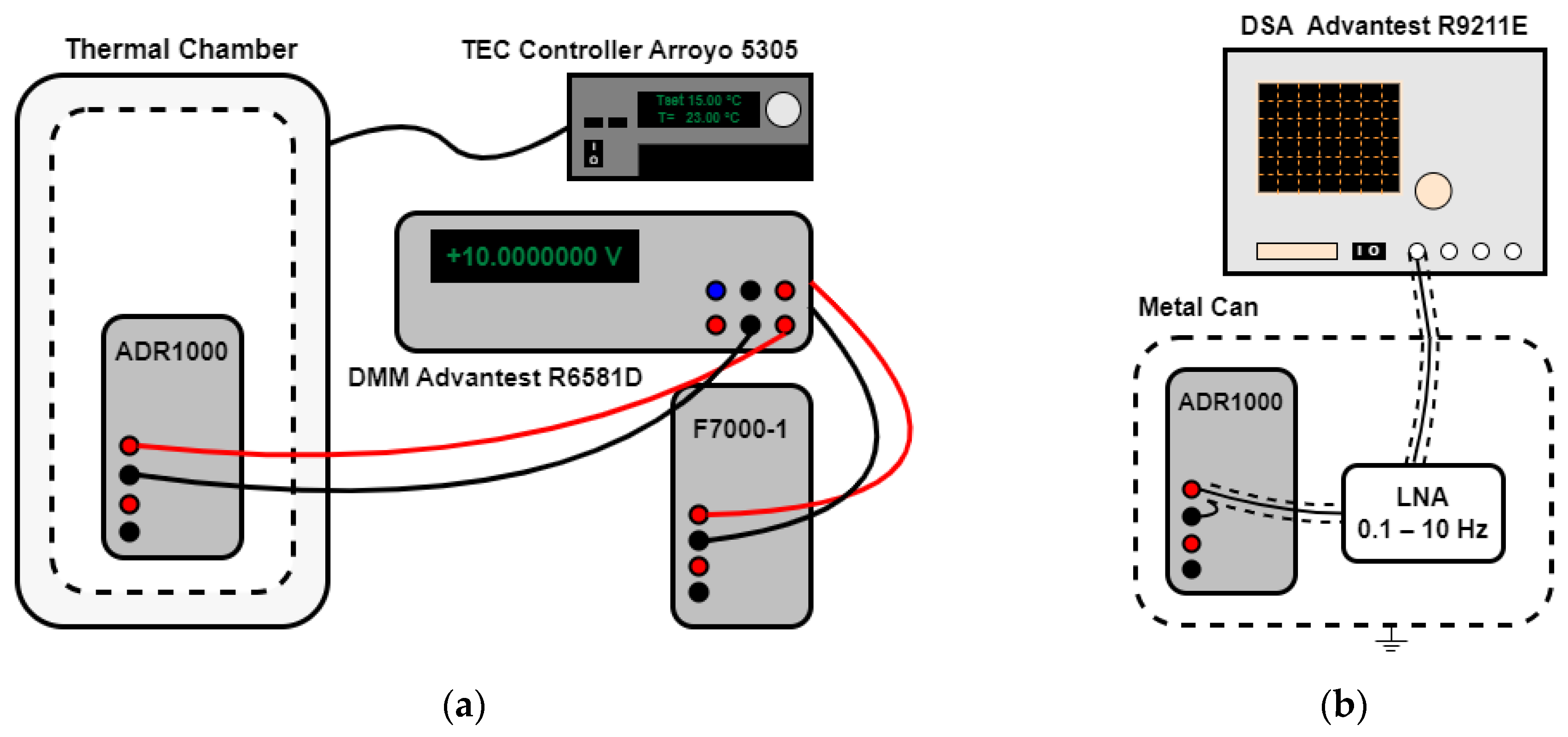
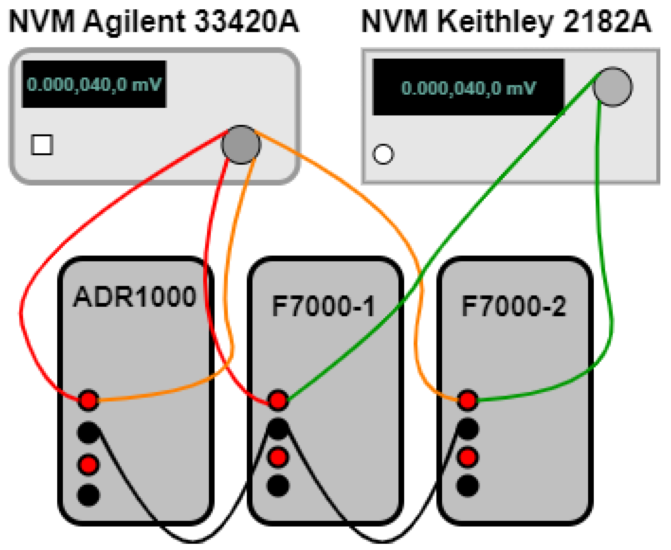
2.2. Procedure and Equipment

In Figure 3, the procedure for determining the z.t.c. temperature and the compensation of the temperature is shown. This procedure is suitable for references with the oven integrated on the chip. For the determination of the z.t.c. temperature, a temperature sweep in a thermal chamber is conducted with the oven on the reference chip turned off. By plotting the change in Zener voltage that can be monitored at the output of IC1 over the temperature in the thermal chamber, an area of the curve can be detected where the Zener voltage does not change with changes in temperature of the chamber. The curve is horizontal in this area, which means the slope in this point is zero. The temperature of the thermal chamber is correlated with the voltage of the internal temperature sensor on the reference chip. The temperature of the temperature diode inside the voltage reference can be measured at the input of IC2. This voltage is used as the setting parameter for the oven to operate it at its z.t.c. temperature. As this voltage and therefore the operating temperature are known, the oven can be tuned to operate at this specific voltage. It is desired that the voltage reference only have a small t.c, ideally, zero t.c. Therefore, another temperature sweep is conducted with the oven turned on. By plotting the change in Zener voltage over the temperature of the chamber and fitting the data to, e.g., a linear model, the t.c. can be derived. To decrease the t.c., resistor R_TC is introduced and adjusted. Several iterations can be performed to improve the t.c. to close to zero, resulting in a temperature-compensated voltage reference operating at its z.t.c. temperature.
Figure 4a shows a block diagram of the setup used for measuring the t.c. The reference board is located inside a thermal chamber, which is controlled via an Arroyo Instruments (San Luis Obispo, CA, USA) 5305 TECSource controller that is connected to a Raspberry Pi via USB. The change in voltage of the reference board is measured by an ADCMT (Namegawa, Japan) R6581D DMM, to which the standard is connected via the front terminals. A Fluke Corporation (Everett, WA, USA) 7000 is connected to the rear terminals of the DMM, which itself is connected to a Raspberry Pi that logs the data via a GPIB-USB-adapter.
In Figure 4b, the setup for measuring low-frequency noise, including the test equipment being used, is depicted. The Advantest Corporation (Tokyo, Japan) Digital Signal Analyzer (DSA) R9211E is connected to a Raspberry Pi via a GPIB-USB adapter. The reference board and the low-noise amplifier (LNA) are located inside a metal can acting as a shield, and the reference board is powered by batteries.
Figure 5 shows the block diagram of the test setup used for observing long-term stability. It consists of two commercial and well-aged voltage standards type Fluke 7000, and all differences are measured with fixed polarity by nanovoltmeters (NVMs) due to the lack of a low thermal electromotive force (t.e.m.f.) scanner. The setup was inspired by [38]. The transfer standard prototype with ADR1000 as the voltage reference and the first F7000 voltage standard are connected to channel 1, and the transfer standard prototype and the second F7000 are connected to channel 2 of an NVM Agilent 34420A measuring their differences. The difference between the first and the second F7000 is measured by an NVM Keithley 2182A. Both NVMs are connected to a Raspberry Pi that logs the data via a GPIB-USB adapter.

3. Results

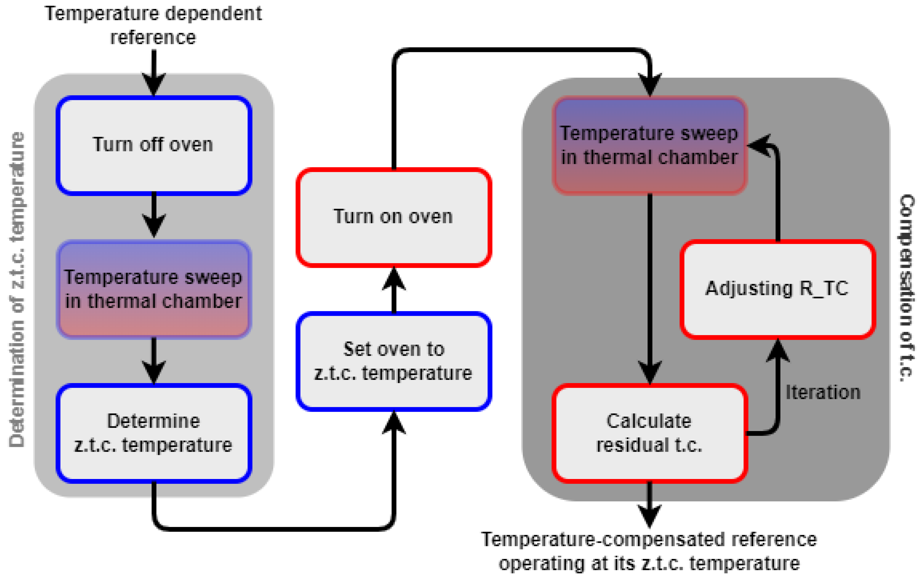
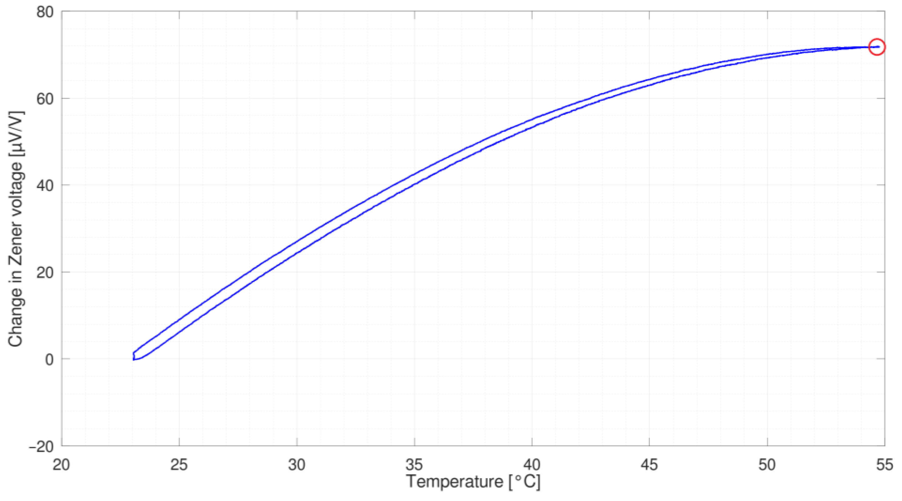
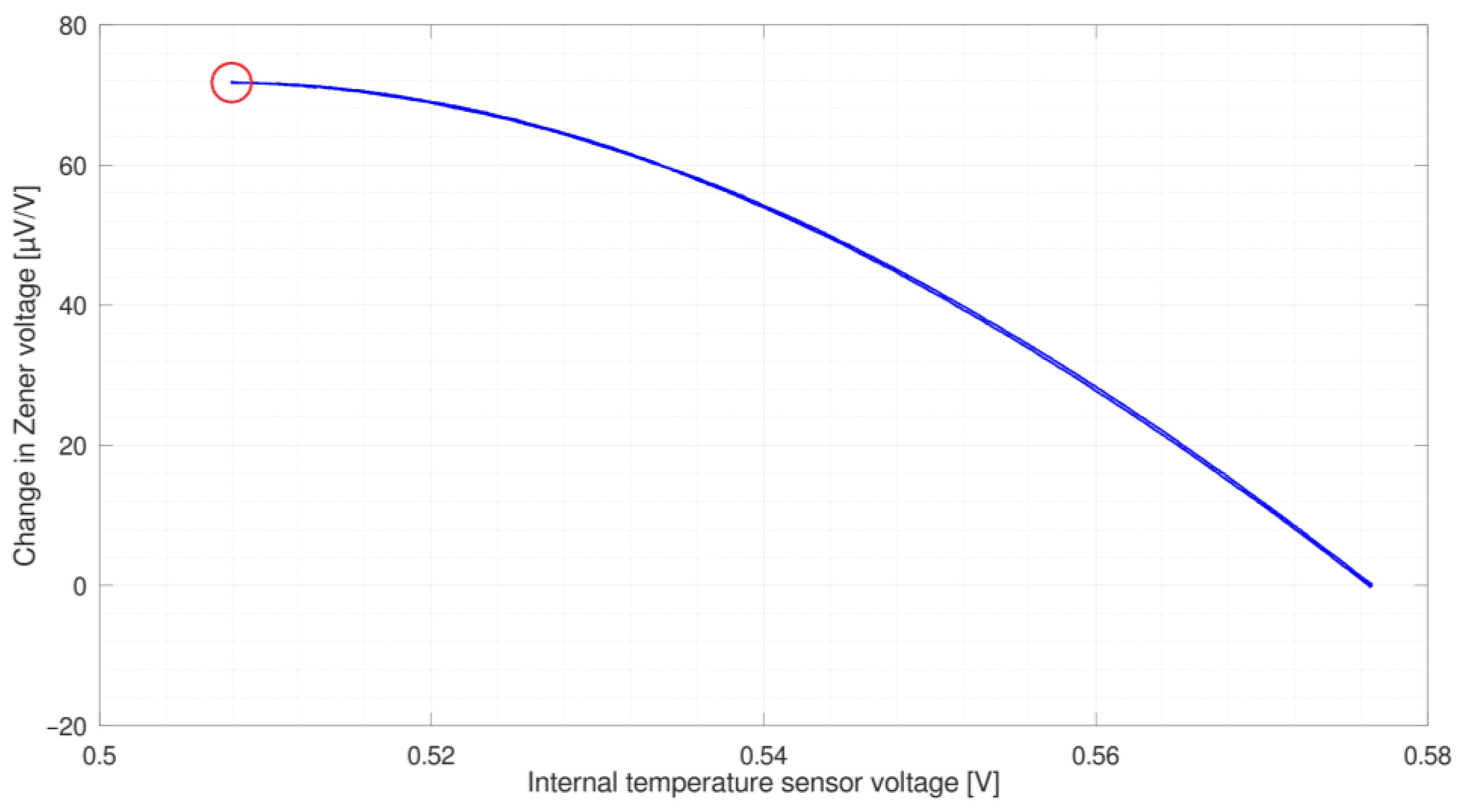
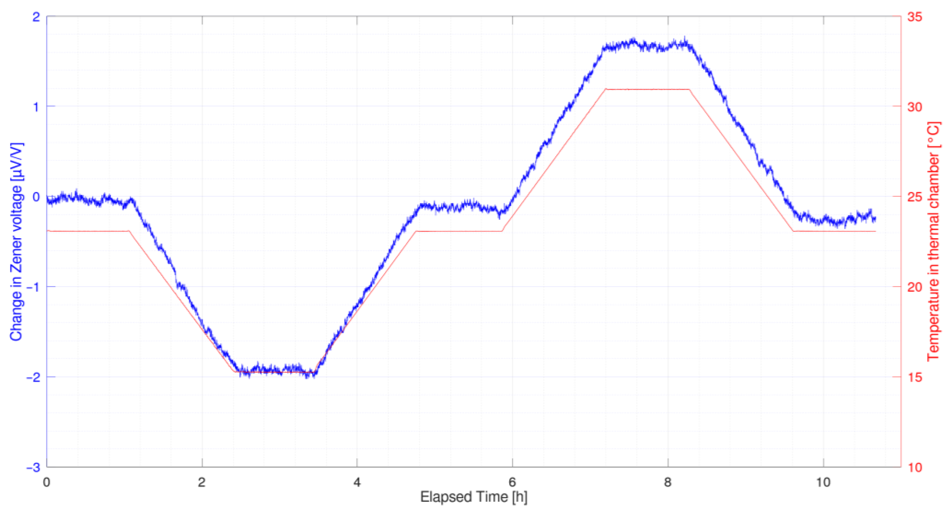
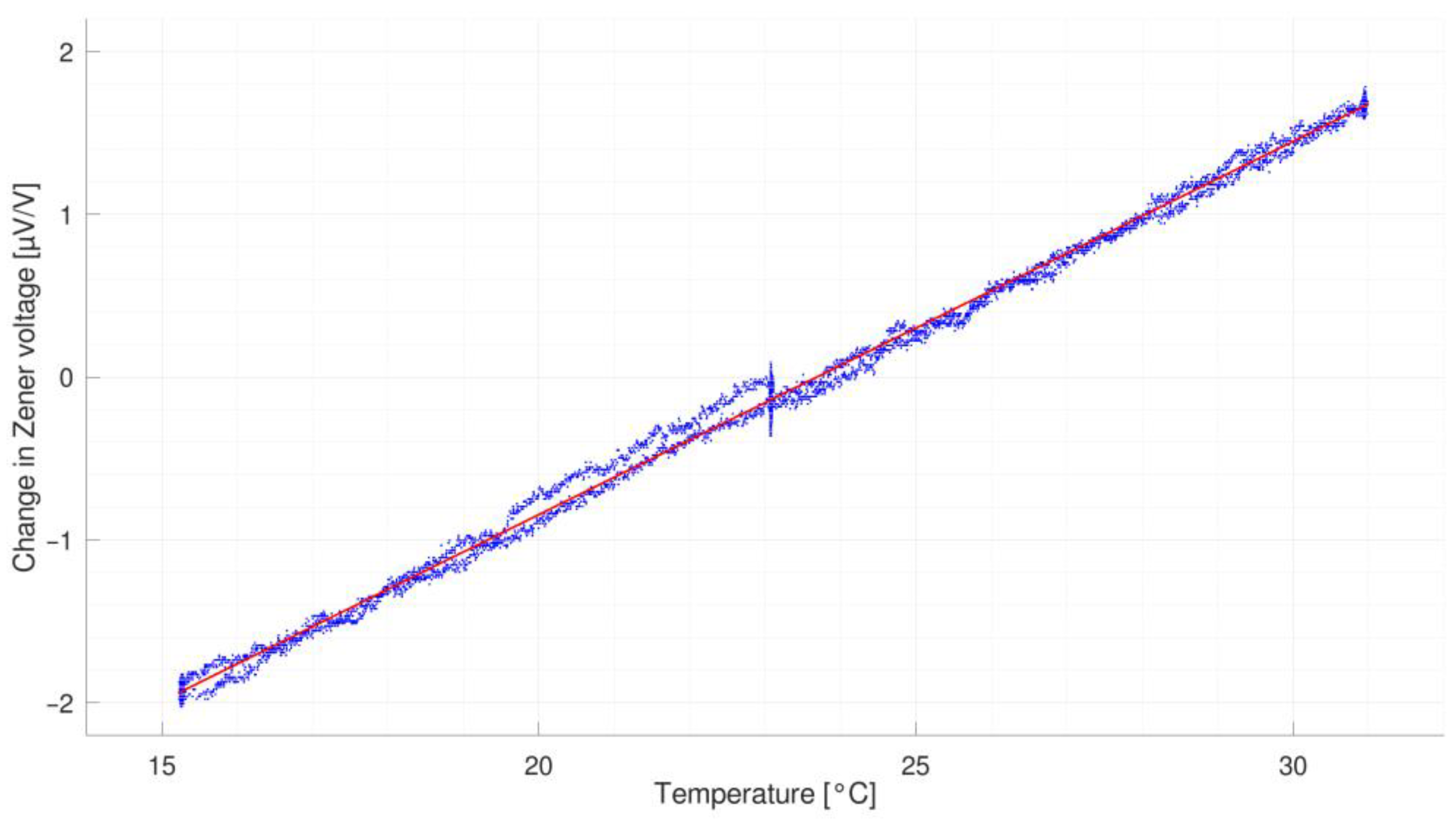
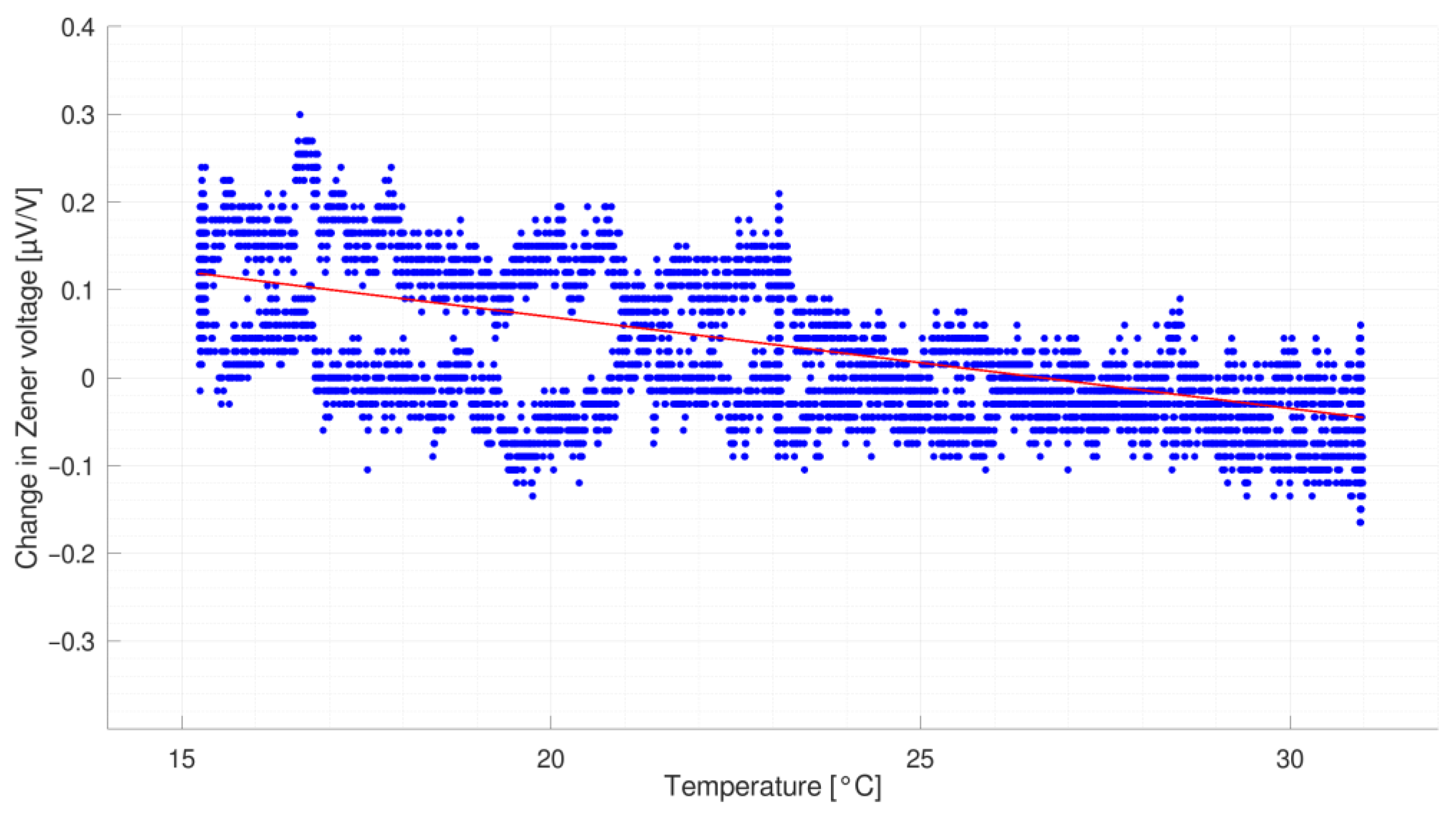
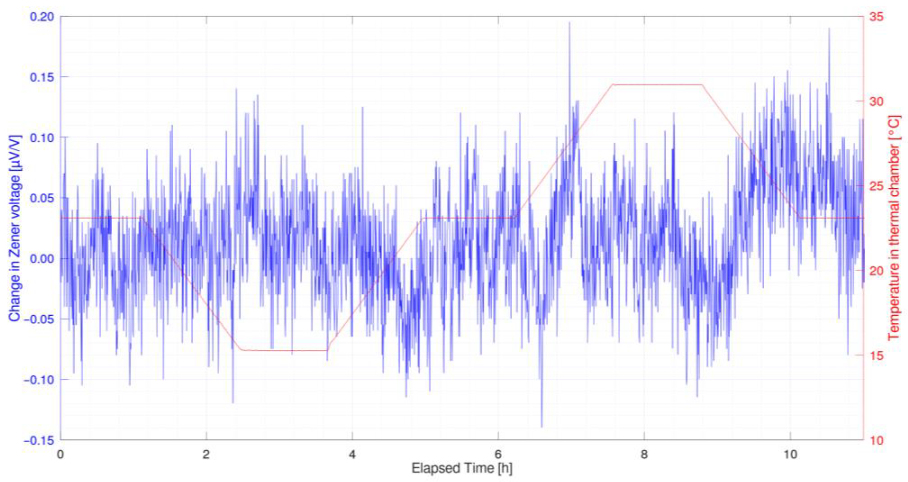
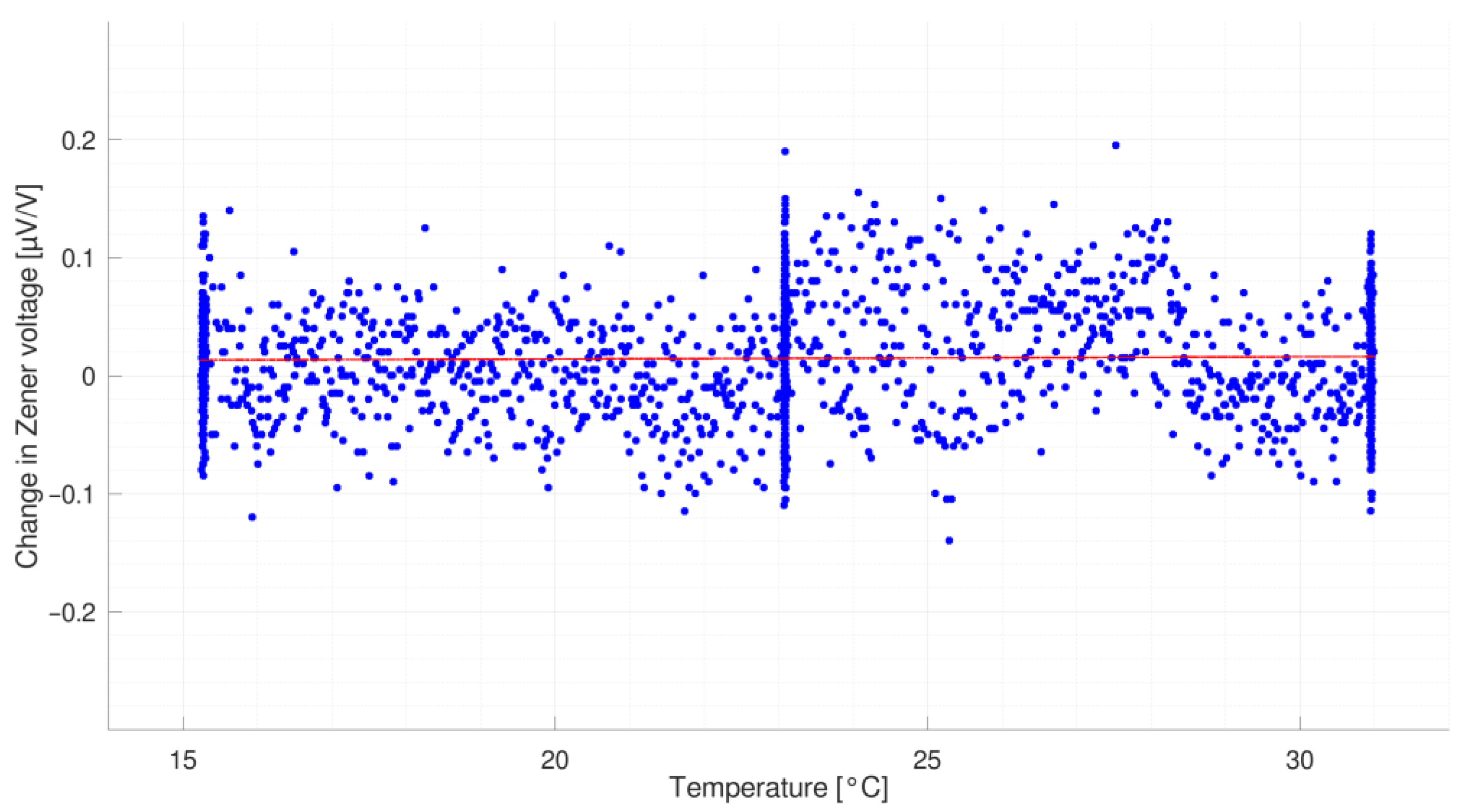
3.1. Temperature Coefficient

To determine z.t.c. temperature and t.c., the procedure from Figure 3 was applied. To set up the reference, the board of the transfer standard prototype was populated with the minimal necessary number of components, that is, the Zener diode, with its required components, including IC3, configured as a buffer. The oven of the Zener was turned off by placing a link at the base of transistor Q1 to ground. The reference board was then put into a thermal chamber and a temperature sweep was performed, while the Zener voltage and the voltage of the temperature-sensing diode were monitored.
Figure 6 reflects the change in Zener voltage over the temperature of the thermal chamber, while Figure 7 shows the same plot over the measured voltage of the internal temperature sensor. During the measurement, the humidity was 53.8 ± 1.2 %rH and the ambient pressure was 991.78 ± 0.3 hPa. As can be seen, the z.t.c. temperature was found to be ~55 °C, which equals a voltage of the internal temperature sensor of 508 mV and is highlighted by the red circles.
Afterwards, the oven was turned on, with the reference being operated at the above-found z.t.c. temperature. This was carried out by adjusting the voltage divider R4/R5 by means of fine trimming R15 to read a voltage of exactly 508 mV at the input of IC2. According to Figure 6 and Figure 7, the oven temperature could then be expected to be ~55 °C. The remaining t.c. of the reference board with the oven of the reference turned on was then measured by performing another temperature sweep, with the measured change in output voltage over time and the temperature profile over time shown in Figure 8 and the change in output voltage over temperature shown in Figure 9. During the sweep, the humidity was measured to be 56.8 ± 0.8 %rH and the ambient pressure was 989.45 ± 0.43 hPa. After applying a linear fit with
u ( T ) = α · T ,
where ∆u is the change in Zener voltage in µV/V, T is temperature in °C, and α is t.c. in µV/V/K, to the measured data in Figure 10 (red curve), a remaining t.c. of α = 0.229 µV/V/K was found.
The dwell time at 15 °C, 23 °C, and 31 °C explains the artifacts visible in the t.c. plots provided in Figure 9 and following figures showing change in Zener voltage over temperature. A comparison of the voltage reading of the internal temperature-sensing diode with the temperature of the thermal chamber revealed that the majority of this residual t.c. was coming from the surrounding circuitry and traces of the reference board and not from the reference itself, as it showed no change over temperature.
Introducing and adjusting R_TC in series to R13 resulted in a reduction in the t.c. down to α = −0.01 µV/V/K, as shown in Figure 10, with humidity measured to be 60.6 ± 0.7 %rH and ambient pressure 985.96 ± 0.33 hPa. At such low levels, it was unclear whether the t.c. was coming from the reference board itself or the used meter with which the measurements were taken.
Therefore, a temperature sweep was performed on the reference board, comparing it directly to a Fluke 7000 sitting at room temperature. During this temperature sweep, the humidity was measured to be 60.47 ± 0.5 %rH and the ambient pressure was 985.76 ± 1.18 hPa.
As shown in Figure 11 and Figure 12, the t.c. almost completely vanished in the observed temperature range of 15 to 31 °C, which proves that in the aforementioned measurement the t.c. of the DMM influenced the result.
Finally, a gain of ~1.5 was added to the output buffer IC3 using a TDP1603 resistor network since they are known to exhibit low noise [39]. We made use of the statistical approach as described in [40]. Consequent trimming of one of the resistor elements within the network by adding RN73 series resistors adjusted the output voltage to 10 V. The resistors used are specified to have a t.c. of 10 ppm/K, so their overall contribution to the t.c. of the resistor in the network should have been neglectable. This, however, led to an additional t.c. that had to be compensated again by adjusting R_TC. The final t.c. of the voltage standard is provided in Figure 13, showing a linear fit (green curve) with a slope of α = 0.003 µV/V/K. As can be seen, the gain stage also added some quadratic portion to the overall t.c. with a square fit (red curve):
u ( T ) = α · T + β · T 2 ,
giving β = −0.003 µV/V/K² and α = 0.147 µV/V/K. The humidity during this measurement was 61.7 ± 0.8 %rH and the ambient pressure was 983.09 ± 0.41 hPa.
Although larger than before, the t.c. was still small for the typical 23 ± 5 °C temperature range of a laboratory environment.

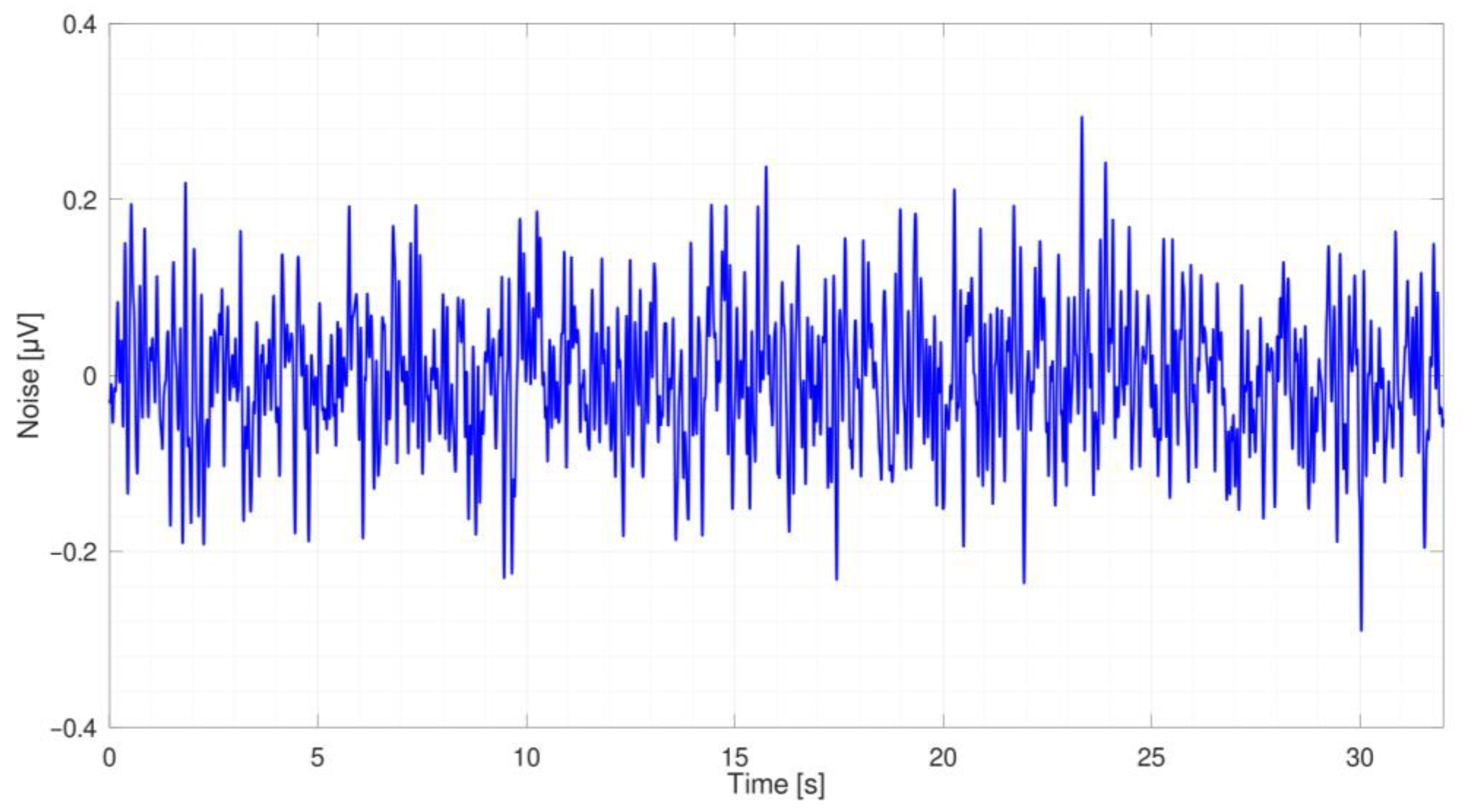
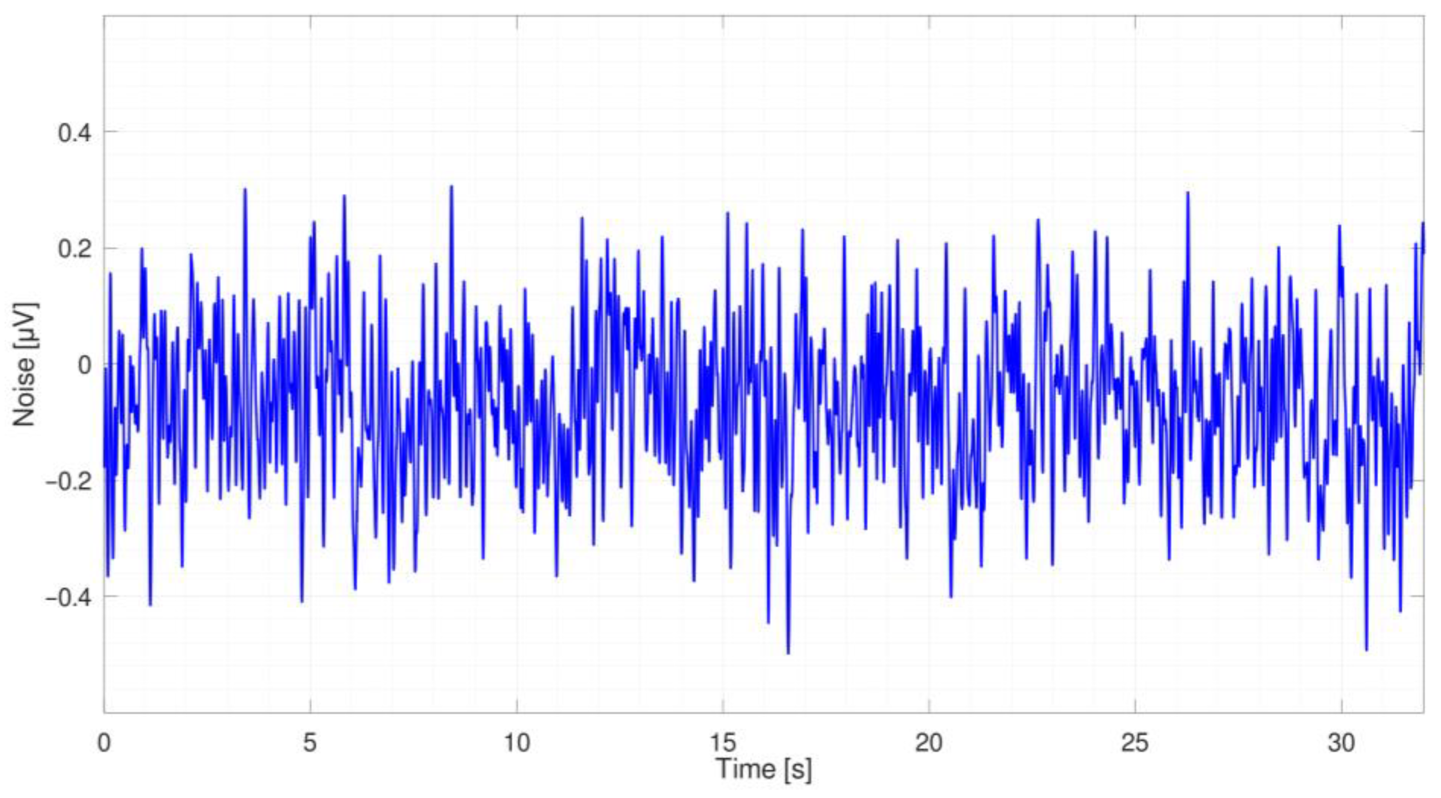
3.2. Noise Measurements

Low-frequency noise measurements of the buffered Zener voltage using an LNA, as depicted in Figure 4b, for the range of 0.1–10 Hz were performed over a course of 32 s. In datasheets of voltage references, a typical time span of 10 s is provided. However, more than one 10 s interval is desirable to see whether there is any popcorn noise present.
Therefore, the reference board was battery operated to prevent common mode noise and was put together with an LNA inside a metal can. The LNA has a noise floor of <100 nVp-p and amplifies the voltage noise by 80 dB. It is connected to the DSA, which captures an interval of 32 s in the time domain.
A noise of ~76 nVrms or ~584 nVp-p was obtained, as depicted in Figure 14, which is well below the value of 900 nVp-p provided in the datasheet for the ADR1000.
Finally, Figure 15 shows the low-frequency noise of the amplified 10 V output. A noise of ~143 nVrms or ~805 nVp-p was obtained, which is well within the expected order for the amplified Zener voltage.
From this point on, the 10 V reference board with ADR1000 was constantly powered by an ultra-low-noise lab power supply based on an R-core transformer and 3x LT3045 in parallel, while the F7000s were sitting in a F7000T rack, powered by the original Hitron 12.88 V linear wall adapter.

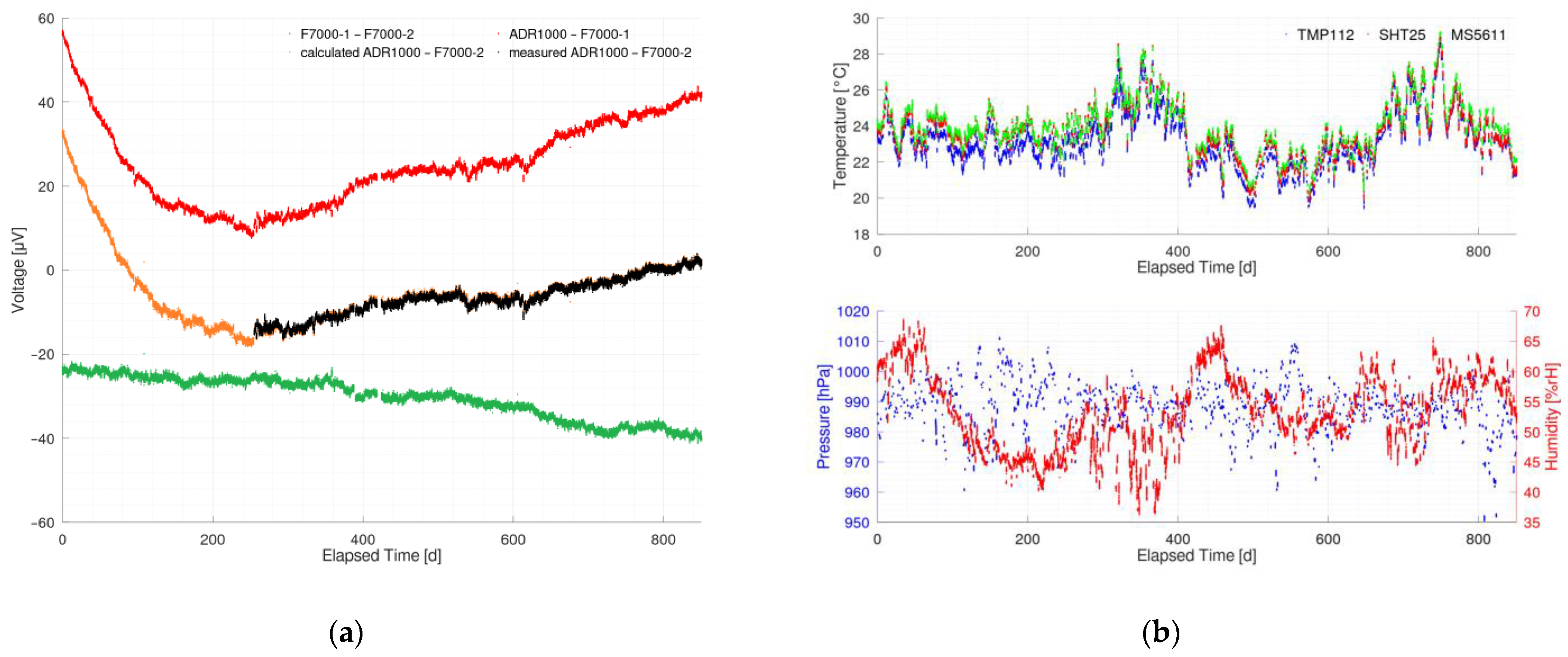
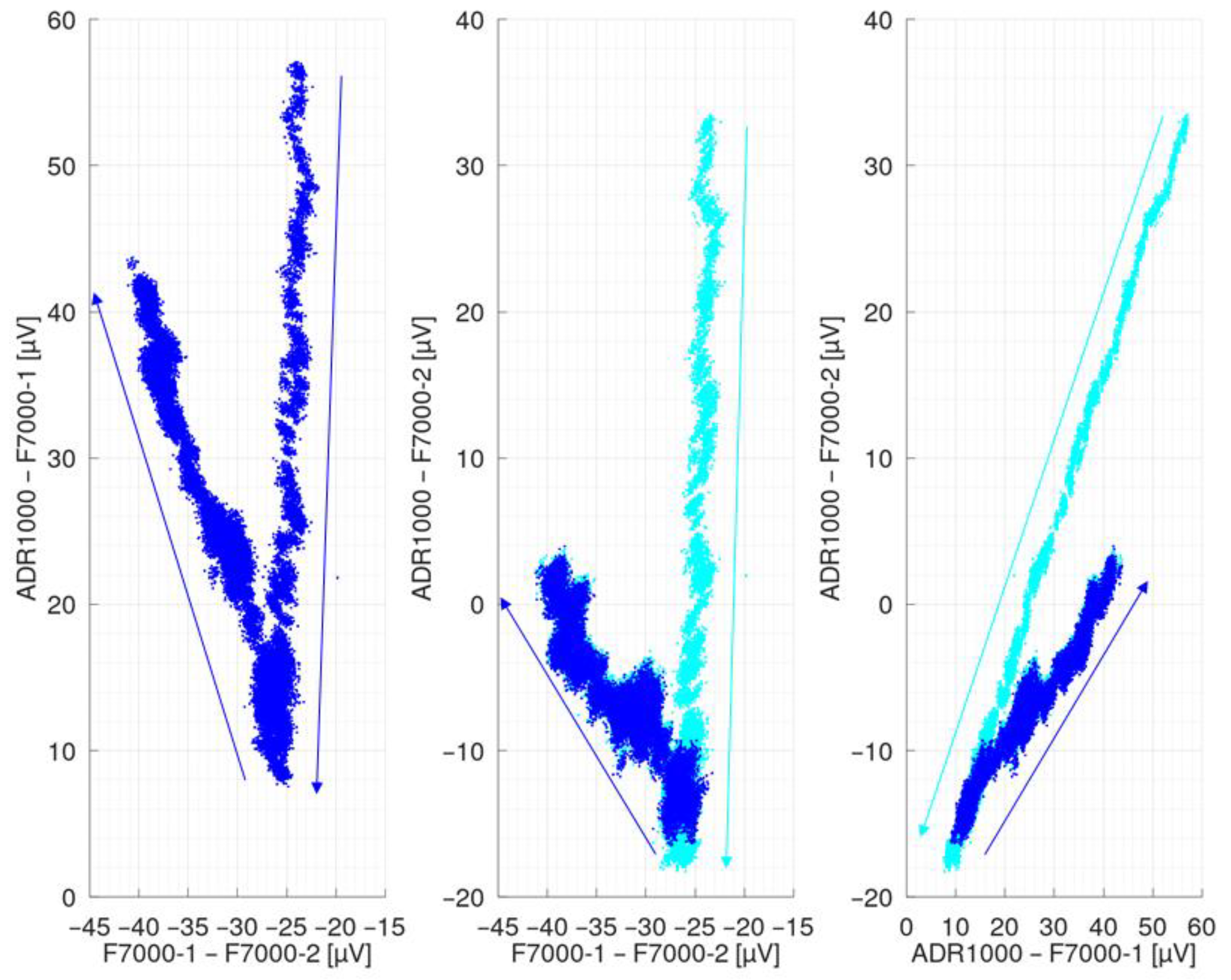
3.3. Long-Term Stability

Long-term drift was observed over a course of 850 days according to [41] and inspired by the procedure in [38] for clocks.
During the first 250 days, only the differences between F7000-1 and F7000-2 (green curve) as well as the difference between ADR1000 and F7000-1 (red curve) were measured using two Keithley 2182As due to the lack of a t.e.m.f. scanner. The orange curve in Figure 16 reflects a calculated difference for ADR1000 and F7000-2. With the presence of another NVM, the setup was rearranged using a Keithley 2182A measuring the difference between F7000-1 and F7000-2 and an Agilent 34420A measuring the difference between ADR1000 and F7000-1 on channel 1 and the difference between ADR1000 and F7000-2 on channel 2, as depicted in Figure 5. The results of this long-term observation are provided in Figure 16a, while the ambient conditions during this measurement are provided in Figure 16b.
In Figure 17, the differences of these measurements are plotted against each other, showing that the measured and the calculated differences, besides minor variations due to noise, match very well. Furthermore, the initial drift of the transfer standard prototype is clearly visible, additionally highlighted by the arrows in the diagrams to indicate the trend direction, which changed after 250 days.

4. Discussion

The noise of the buffered Zener voltage as well as the 10 V output are remarkably low for a single Zener-based voltage standard. The numbers exceed the expectations and are exceptionally good in comparison to existing commercial voltage references and standards.
The overall t.c. of the 10 V output after proper t.c. compensation is judged to be very low and neglectable for use in a normal 23 °C laboratory environment. However, the statistical resistor network added a quadratic portion to the overall t.c., which is unexpected. The reason for that might be investigated and found to be an uneven power distribution within the network. This is the reason why we suggest connecting the resistors in an interdigital fashion to handle this.
Next, long-term drift was observed. During the first 250 days, the low-noise solid-state 10 V transfer standard settled before an additional drift mechanism took over, which then led to a drift in the opposite direction. It is yet unclear whether this drift is related to the voltage reference itself or the statistical resistor network. Since the Zener voltage and ground star-points are accessible, we aim to add a piggyback board with a buffer stage for the raw Zener voltage. By measuring the difference between the buffered Zener voltage and 10 V output, the root cause for the drift can be ruled out.
For the long-term observation, a method according to [41] was used, though without polarity reversal due to the lack of a low t.e.m.f. scanner and using two nanovolt meters instead. One might argue that this might be an improper way of measuring the differences, as t.e.m.f. voltages do not cancel out, and that common mode jumps, which means that all three voltage standards jump by the same amount in the same direction, are not covered by such measurements. However, the ambient temperature was rather constant during the observation, and it is rather unlikely that all three standards jump in the same direction, as they can be assumed to be uncorrelated. The absence of a correlation can be explained by noting that F7000-1 was manufactured post year 2000, with its DC-DC converter based on LT1533, while F7000-2 was manufactured prior to year 2000, with a discrete built DC-DC converter [42,43,44,45]. The LTZ1000 references in both F7000 have different dates of manufacturing and should thus be uncorrelated to a large extent. The third voltage standard is based on the ADR1000, with a different manufacturing process made in a different fab, which underlines the argument.
The initial drift of the reference finished roughly after 250 days of observation time. From there on, a different drift mechanism took over, reversing the drift direction. This drift could be related to the resistor network of the 10 V gain stage and/or the reference itself, though no correlation to changes in humidity or temperature were observed.
Although the datasheet for the ADR1000 claims a drift of 0.5 ppm/year after the first 3000 h, we observed a longer period for the first stabilization and a drift in the opposite direction of ~−16 µV in the 800 days afterwards, without signs of settling just yet. The time for the longer initial drift could be due to the fact that the reference is operated at 55 °C instead of the 75 °C given in the datasheet. A rule of thumb based on the Arrhenius equation predicts a doubling to quadruplication of the reaction velocity for an increase in temperature of 10 K. Thus, the observed stabilization period of ~6000 h is well within these expectations, given that the reference did not undergo a burn-in procedure, as described for LTZ1000 in [46].
A comparison of the transfer standard prototype in this work to two selected commercial standards from Table 1 is given in Table 3. A t.c. smaller than Fluke 732C and Wavetek/Fluke 7000 for our prototype was obtained, with exceptionally good low-frequency noise.

5. Conclusions

A low-noise, low-t.c., solid-state 10 V transfer standard prototype based on ADR1000 for laboratory use was presented. The drift of the transfer standard prototype is still large and nowhere near the datasheet value given for the voltage reference.
The impact of the 10 V gain stage is unclear, hence why we propose implementing a buffered Zener output and, in addition, a separate 10 V gain stage output. By measuring the difference between both, the effects of t.c. and long-term drift can be ruled out. Different resistor networks and resistor schemes within the network for the 10 V gain stage should be tested to identify the ones with the lowest impact on t.c. and drift but also to test several different amplifier solutions, such as PWM-based ones, to avoid resistors completely.
Furthermore, we suggest treating the t.c. adjustment of the Zener voltage and the 10 V gain stage separately. Thus, the t.c. of the Zener voltage could be adjusted by R_TC, which resulted in very low temperature residues, as shown. For the 10 V gain stage, another location within the circuit has to be identified.
Some of the aforementioned aspects will be addressed in the future. It is planned to build more but slightly modified samples of the proposed transfer standard prototype considering the achieved findings.
We additionally plan to investigate the impact of the oven temperature on initial reference drift, as the drift value given in the datasheet of ADR1000 is specified for a reference operated at a 75 °C oven temperature. The aim is to apply the aforementioned procedure to identify z.t.c. temperature first; to adjust the remaining t.c. second; to then operate the oven of the voltage reference at a higher temperature, e.g., at 75 °C or 100 °C, to accelerate the initial drift until it has settled; and to then set back the oven to the previously found z.t.c. temperature. In this context, larger temperature ranges, extending temperatures below 15 °C and above 31 °C, could be investigated.

Author Contributions

Conceptualization, A.B.; methodology, A.B.; software, A.B.; validation, A.B. and D.W.; formal analysis, A.B.; investigation, A.B.; resources, A.B.; data curation, A.B. and D.W.; writing—original draft preparation, A.B. and D.W.; writing—review and editing, A.B. and D.W.; visualization, A.B. and D.W.; supervision, A.B., D.W. and A.Z.; project administration, A.B. All authors have read and agreed to the published version of the manuscript.

Funding

This research received no external funding.

Data Availability Statement

Data are contained within the article.

Conflicts of Interest

The authors declare no conflicts of interest.

References

  1. Elmquist, R.E.; Cage, M.E.; Tang, Y.H.; Jeffery, A.M.; Kinard, J.R., Jr.; Dziuba, R.F.; Oldham, N.M.; Williams, E.R. The ampere and electrical standards. J. Res. Natl. Inst. Stand. Technol. 2001, 106, 65. [Google Scholar] [CrossRef] [PubMed]
  2. Hamer, W.J. Standard Cells: Their Construction, Maintenance, and Characteristics; US Government Printing Office: Washington, DC, USA, 1965; Volume 84.
  3. Schlamminger, S.; Abbott, P.; Kubarych, Z.; Jarrett, D.; Elmquist, R. The units for mass, voltage, resistance, and electrical current in the SI. IEEE Instrum. Meas. Mag. 2019, 22, 9–16. [Google Scholar] [CrossRef]
  4. Rüfenacht, A.; Fox, A.E.; Butler, G.E.; Burroughs, C.J.; Dresselhaus, P.D.; Schwall, R.E.; Cular, S.; Benz, S.P. Compact DC Josephson Voltage Standard. In Proceedings of the 2020 Conference on Precision Electromagnetic Measurements (CPEM), Denver, CO, USA, 24–28 August 2020; IEEE: Washington, DC, USA, 2020; pp. 1–2. [Google Scholar] [CrossRef]
  5. Maruyama, M.; Urano, C.; Kaneko, N.-H.; Sannomaru, E.; Yonezawa, T.; Kanai, T.; Yoshida, H.; Yoshino, Y. Development of a compact Zener DC voltage standard with detachable module system. In Proceedings of the 2016 Conference on Precision Electromagnetic Measurements (CPEM 2016), Ottawa, ON, Canada, 10–15 July 2016; IEEE: Washington, DC, USA, 2016. [Google Scholar] [CrossRef]
  6. Maruyama, M.; Urano, C.; Kaneko, N.-H.; Yonezawa, T.; Kanai, T.; Sannomaru, E.; Honjo, J.; Yoshino, Y. Investigation of atmospheric-pressure dependence of compact detachable Zener module. In Proceedings of the 2018 Conference on Precision Electromagnetic Measurements (CPEM 2018), Paris, France, 8–13 July 2018; IEEE: Washington, DC, USA, 2018; pp. 1–2. [Google Scholar] [CrossRef]
  7. Meléndez, R.; Solano, A.; Sánchez, H. Zener DC Voltage Standard Shutdown Behavior. In Proceedings of the 2018 Conference on Precision Electromagnetic Measurements (CPEM 2018), Paris, France, 8–13 July 2018; IEEE: Washington, DC, USA, 2018; pp. 1–2. [Google Scholar] [CrossRef]
  8. Capra, P.P.; Cerri, R.; Galliana, F.; Lanzillotti, M. 10 V, 1 Ω, 10 kΩ high accuracy standard setup for calibration of multifunction electrical instruments and for inter-laboratory comparisons. In Proceedings of the 18th International Congress of Metrology, Paris, France, 18 September 2017; EDP Sciences: Les Ulis, France, 2017; p. 07006. [Google Scholar] [CrossRef]
  9. Power, O.; Walsh, J.E. Investigation of the long-and medium-term drift of Zener diode-based voltage standards. IEEE Trans. Instrum. Meas. 2005, 54, 330–336. [Google Scholar] [CrossRef]
  10. Manual User’s Handbook for the Datron 4910 and 4911 DC Voltage Reference Standards; Datron/Wavetek: San Diego, CA, USA, 1990; pp. 3–4.
  11. Manual Model 730A; DC Transfer Standard. John Fluke MFG. Co., Inc.: Seattle, WA, USA; pp. 1-1–1-3.
  12. Manual Model 731A; DC Transfer Standard. John Fluke MFG. Co., Inc.: Seattle, WA, USA; pp. 1-1–1-2.
  13. Manual Model 731B; DC Transfer Standard. John Fluke MFG. Co., Inc.: Mountlake Terrace, WA, USA, 1974; pp. 1–2.
  14. Manual Model 732A; DC Reference Standard. John Fluke MFG. Co., Inc.: Everett, WA, USA, 1986; p. 1-1.
  15. Manual Model 732B/734A; DC Reference Standard. Fluke Corporation: Everett, WA, USA, 1997; pp. 1-7–1-8.
  16. Manual Model 732C/734C; DC Reference Standard. Fluke Calibration: Everett, WA, USA, 2018; pp. 5–6. Available online: https://s3.amazonaws.com/download.flukecal.com/pub/literature/6010864a-fcal-datasheet-w.pdf (accessed on 18 December 2023).
  17. DC Reference & Transfer Standards, Automated Voltage Measurement System; Fluke Corporation: Everett, WA, USA, 2000; p. 4.
  18. Manual Portable DC Voltage Standard, Model 4410; Guildline Instruments Inc.: Orlando, FL, USA; p. 2.
  19. Manual 3000ZR Precision Voltage Standard, Operation Manual; Transmille Ltd.: Kent, UK, 2013; Version 3.00; p. 10. Available online: https://transmillecalibration.com/wp-content/uploads/2018/05/3000ZR-Operation-Manual-V2-00.pdf (accessed on 17 December 2023).
  20. Manual Valhalla Scientific, 2720GS Ultra-Precision Direct Voltage System; pp. 3–6. Available online: http://www.ko4bb.com/manuals/141.70.193.22/Valhalla_Scientific_2720GS_Ultra-Precision_DC_Voltage_System_Calibrator_Service_Manual.pdf (accessed on 18 December 2023).
  21. Walters, K.; Clark, M. An Introduction to Zener Diodes, MicroNotes Series No. 201. Microsemi Scottsdale. Available online: https://www.microsemi.com/document-portal/doc_view/14613-an-introduction-to-zener-diodes (accessed on 18 December 2023).
  22. Walters, Kent, Microsemi Scottsdale, Zero-Temperature Coefficient Reference Diodes, MicroNotes Series 205. 1997. Available online: https://www.microsemi.com/document-portal/doc_view/14616-zero-tc-reference-diodes (accessed on 18 December 2023).
  23. Richard, K. Linear Technology LTFLU. Available online: https://www.richis-lab.de/REF04.htm (accessed on 19 December 2023).
  24. Richard, K. Linear Technology LTFLU (Alibaba). Available online: https://www.richis-lab.de/REF25.htm (accessed on 19 December 2023).
  25. Richard, K. Motorola SZA263. Available online: https://www.richis-lab.de/REF24.htm (accessed on 19 December 2023).
  26. Bülau, A. Setting up a SZA263/LTFLU Voltage Reference. Available online: https://xdevs.com/article/ltflu_ref/ (accessed on 18 December 2023).
  27. Deaver, D. Predictability of Solid State Zener References. In Proceedings of the Measurement Science Conference, Anaheim, CA, USA, 18–19 January 2001. [Google Scholar]
  28. Ilić, D.; Šala, A.; Lenicek, I. Prediction of the Output Voltage of DC Voltage Standards. In Proceedings of the XIX IMEKO World Congress Fundamental and Applied Metrology, Lisbon, Portugal, 6–11 September 2009; Volume 1, pp. 601–606. [Google Scholar]
  29. Hamilton, C.A.; Tarr, L.W. Projecting Zener DC Reference Performance between Calibrations. IEEE Trans. Instrum. Meas. 2003, 52, 454–456. [Google Scholar] [CrossRef]
  30. Spreadbury, P.J. The Ultra-Zener… is it a portable replacement for the Weston cell? Meas. Sci. Technol. 1990, 1, 687. [Google Scholar] [CrossRef]
  31. Datasheet Linear Technology Corporation, LM129/LM329, 6.9V Precision Voltage Reference, Rev D Dec. 2014. Available online: https://www.analog.com/media/en/technical-documentation/data-sheets/129329fd.pdf (accessed on 18 December 2023).
  32. Datasheet National Semiconductor, LM199/LM299/LM399 Precision Reference, April 2005. Available online: https://www.symres.com/files/LM399.pdf (accessed on 18 December 2023).
  33. Datasheet Linear Technology Corporation, LM199/LM399, LM199A/LM399A Precision Reference, Rev C Dec. 2014. Available online: https://www.analog.com/media/en/technical-documentation/data-sheets/199399fc.pdf (accessed on 18 December 2023).
  34. Datasheet Linear Technology Corporation, LTZ1000/LTZ1000A Ultra Precision Reference, LT 1115 Rev E Nov. 2015. Available online: https://www.analog.com/LTZ1000/datasheet (accessed on 18 December 2023).
  35. Datasheet Analog Devices, Inc. ADR1399, Oven-Compensated, Buried Zener, 7.05 V Voltage Reference, Rev. A, March 2022. Available online: https://www.analog.com/ADR1399/datasheet (accessed on 18 December 2023).
  36. Datasheet Analog Devices, Inc. ADR1000, Oven-Compensated, Buried Zener, 6.62 V Voltage Reference, Rev. B, March 2022. Available online: https://www.analog.com/media/en/technical-documentation/data-sheets/adr1000.pdf (accessed on 1 November 2023).
  37. Marusenkov, A. Possibilities of further improvement of 1-second fluxgate variometers. Geosci. Instrum. Methods Data Syst. 2017, 6, 301–309. [Google Scholar] [CrossRef]
  38. Vernotte, F.; Addouche, M.; Delporte, M.; Brunet, M. The Three Cornered Hat Method: An Attempt to Identify Some Clock Correlations. In Proceedings of the 2004 IEEE International Frequency Control Symposium and Exposition, Montreal, QC, Canada, 24–27 August 2004; IEEE: Washington, DC, USA, 2004; pp. 482–488. [Google Scholar]
  39. Walter, D.; Bülau, A.; Zimmermann, A. Review on Excess Noise Measurements of Resistors. Sensors 2023, 23, 1107. [Google Scholar] [CrossRef] [PubMed]
  40. Fluke Calibration. A Practical Approach to Maintaining DC Reference Standards. Available online: https://www.elcal.ch/files/11749-eng-01-a.pdf (accessed on 19 December 2023).
  41. Eicke, W.G.; Cameron, J.M. Designs for Surveillance of the Volt Maintained by a Small Group of Saturated Standard Cells; US Government Printing Office: Washington, DC, USA, 1967; NBS Technical Note 430.
  42. Pickering, J.R.; Thompson, R.; Williams, J.M. A new compact isolated power supply for electrical metrology at low signal levels. In Proceedings of the BEMC 99–9th International Conference on Electromagnetic Measurement, Brighton, UK, 2–4 November 1999. [Google Scholar]
  43. Williams, J.M.; Smith, D.R.; Georgakopoulos, D.; Patel, P.D.; Pickering, J.R. Design and metrological applications of a low noise, high electrical isolation measurement unit. IET Sci. Meas. Technol. 2009, 3, 165–174. [Google Scholar] [CrossRef]
  44. Pickering, J.R.; Roberts, P. A Solid State DC Reference System. In Proceedings of the NCSL Conference, Dallas, TX, USA, 16–20 July 1995; p. 369. [Google Scholar]
  45. Crisp, P.B. Setting New Standards for DC Voltage Maintenance Systems, CalLab, Sep./Oct. 1999. In Proceedings of the IEE Seminar Measurement Dissemination by Transfer Methods (Ref. No. 1999/048), London, UK, 12 May 1999; IET: Stevenage, UK, 1999. [Google Scholar] [CrossRef]
  46. Cern, Burn in of the Voltage Reference for the 22-bit Delta-Sigma Converter, v. 10.1. 2009. Available online: https://cal.equipment/doc/CERN/1101699_V1_Burn_in_of_LTZ1000.pdf (accessed on 18 December 2023).
Figure 1. Schematic of the voltage standard.
Metrology 04 00007 g001
Figure 2. The 10 V transfer standard prototype with (a) the reference board in the foreground and the prospective power supply board in the background; (b) its enclosure; (c) the opened enclosure with the reference and power supply boards inside.
Metrology 04 00007 g002
Figure 3. Block diagram of the procedure used for determining the z.t.c. temperature and for temperature compensation. The procedure is suitable for references with an oven integrated on the chip.
Metrology 04 00007 g003
Figure 4. Test setup (a) for t.c measurement; (b) for noise measurement.
Metrology 04 00007 g004
Figure 5. Setup for long-term stability measurement. Wire colors are consistent with color of long-term observation plot.
Metrology 04 00007 g005
Figure 6. Measured change in output voltage of the buffered Zener voltage over temperature in the thermal chamber with the oven of the reference itself turned off. The red circle marks the z.t.c. temperature, as the slope of the change in Zener voltage is zero at this point.
Metrology 04 00007 g006
Figure 7. Change in output voltage of the buffered Zener voltage over the measured voltage of the internal temperature sensor during a temperature sweep with the oven of the reference itself turned off. The red circle marks the measured voltage of the internal temperature sensor, as the slope of the change in Zener voltage is zero at this point.
Metrology 04 00007 g007
Figure 8. Measured change in output voltage of the buffered Zener voltage and temperature over time within the thermal chamber during the temperature sweep.
Metrology 04 00007 g008
Figure 9. Measured change in output voltage of the buffered Zener voltage over temperature during a temperature sweep with the oven of the reference itself turned on. The blue curve shows the measured data, while the red curve shows the linear fit applied to them.
Metrology 04 00007 g009
Figure 10. Measured change in output voltage of the buffered Zener voltage over temperature after a first t.c. trimming during a temperature sweep with the oven of the reference itself turned on (blue). The red curve shows a linear fit applied to the data.
Metrology 04 00007 g010
Figure 11. Measured change in output voltage of the buffered Zener voltage and temperature within the thermal chamber during the temperature sweep over time. The influence of the DMM was excluded by comparing the reference board directly to a Fluke 7000.
Metrology 04 00007 g011
Figure 12. Measured change in output voltage of the buffered Zener voltage over temperature after t.c. trimming during a temperature sweep with the oven of the reference itself turned on and with the influence of the DMM excluded (blue). The red curve shows the linear fit.
Metrology 04 00007 g012
Figure 13. Final measured t.c. of the reference board over temperature after trimming the output voltage to 10 V and t.c. compensation (blue). The green curve shows the approach of a linear fit. Better agreement with measured points can be reached with a square fit (red).
Metrology 04 00007 g013
Figure 14. Low-frequency noise (0.1–10 Hz) of the buffered Zener voltage.
Metrology 04 00007 g014
Figure 15. Low-frequency noise (0.1–10 Hz) of the 10 V reference board.
Metrology 04 00007 g015
Figure 16. (a) Long-term observation of all three standards by measuring their differences; (b) ambient conditions showing ambient temperature, relative humidity, and air pressure.
Metrology 04 00007 g016
Figure 17. Differences of two standards each, plotted against each other (cyan dots are calculated data, blue dots are measured data, arrows indicate drift direction).
Metrology 04 00007 g017
Table 1. Commercial 10 V voltage standards and their most important specifications with respect to the 10 V output.
10 V Solid-State Voltage StandardReference ICStability [ppm]T.C. [ppm/°C]NoiseOven
30 d90 d1 y
ADCMT 6900 [5]LTZ1000--20.01-On chip
Datron/Wavetek 4910 [10]LTZ1000CH0.311.50.050.04 ppm rms
(0.01–2 Hz)
On chip
Fluke 730A [11]DH80417B<10Mean of four outputs within 1 ppm of a straight line-0.5 (20–30 °C) <1 (4–40 °C) <1.5 (0–4 and 40–55 °C)<1 ppm p-p
(DC–1 Hz), 20 µVrms
(1 Hz–1 MHz)
None
Fluke 731A [12]DH80417B10--0.5 (20–30 °C)
<1 (4–40 °C) <1.5 (0–4 and 40–55 °C)
<1 ppm p-p
(DC–1 Hz), 20 µV rms
(1 Hz–1 MHz)
Discrete
Fluke 731B [13]DH80417B±10±15±30<1 (10–45 °C)
<2 (0–10 and 45–55 °C)
<1 ppm p-p
(DC–1 Hz), 20 µV rms
(1 Hz–1 MHz)
Except <70 µV rms @ 10 V output
Discrete
Fluke 732A [14]SZA2630.513±0.05 (0–18 °C and 28–40 °C)<1 µV rms
(0.1–10 Hz)
Discrete
Fluke 732B [15]LTFLU-1±0.3±0.8±2<0.04 (15–35 °C)±0.06 ppm rms (0.01–10 Hz)Discrete
Fluke 732C [16]LTFLU-1A±0.3±0.8±2±0.04 (15–35 °C)±0.06 µV/V rmsDiscrete
Wavetek/Fluke 7000/7001
7004N/T
7010N/T
[17]
LTZ1000-
-
-
±0.9
±0.8
±0.7
±1.8
±1.2
±1
<0.05
<0.03
<0.02
(15–35 °C)
<0.1 ppm rms
<0.05 ppm rms
<0.03 ppm rms
(0.01–10 Hz)
On chip
Guildline 4410 [18]8x LM329AH--−3 ± 2
(1st year)
−2 ± 2
(2nd year)
±0.04 (16–28 °C)<0.1 ppm rms
(0.3–10 Hz)
None
Transmille 3000ZR [19]LTZ10000.8-2--On chip
Valhalla 2720GS/54-4T [20]4x LM3993.2 ppm + 2.3 µV @13 V5.3 ppm + 2.3 µV @13 V13.1 ppm + 2.3 µV @13 V0.01 ppm + 0.20 µV @13 V 130 µV rmsOn chip and discrete
Valhalla 2720GS [20]6x LM3992.0 ppm + 2.3 µV @13 V2.6 ppm + 2.3 µV @13 V5.3 ppm + 2.3 µV @13 V0.01 ppm + 0.20 µV @13 V 130 µV rmsOn chip and dis-crete
Valhalla 2720GS/HSR [20]8x LM3991.8 ppm + 2.3 µV @13 V2.1 ppm + 2.3 µV @13 V3.5 ppm + 2.3 µV @13 V0.01 ppm + 0.20 µV @13 V 130 µV rmsOn chip and dis-crete
1 Using internal cal, 0–35 °C.
Table 2. Comparison of different commercially available voltage references used in test equipment.
Voltage ReferenceZener Reference Voltage [V]Zener NoiseTemperature Coefficient [ppm/°C]Long-Term Stability
LM129A [31]Min. 6.7, typ. 6.9, max. 7.2typ. 7 µV, max. 20 µV p-pTyp. 6, max. 1020 ppm/√kHr
LM329A [31]Min. 6.6, typ. 6.9, max. 7.25typ. 7 µV, max. 100 µV p-pTyp. 6, max. 1020 ppm/√kHr
LM199AH (NS) [32]Min. 6.8, typ. 6.95, max. 7.1typ. 7 µV, max. 20 µV p-pTyp. 0.2, max. 0.5Typ. 20 ppm
LM299H (NS) [32]Min. 6.8, typ. 6.95, max. 7.1typ. 7 µV, max. 20 µV p-pTyp. 0.3, max. 1Typ. 20 ppm
LM399H (NS) [32]Min. 6.6, typ. 6.95, max. 7.3typ. 7 µV, max. 50 µV p-pTyp. 0.3, max. 2Typ. 20 ppm
LM399AH (NS) [32]Min. 6.6, typ. 6.95, max. 7.3typ. 7 µV, max. 50 µV p-pTyp. 0.3, max. 1Typ. 20 ppm
LM199 (LT) [33]Min. 6.8, typ. 6.95, max. 7.1typ. 7 µV, max. 20 µV p-pTyp. 0.3, max. 1Typ. 8 ppm/√kHr
LM199A (LT) [33]Min. 6.8, typ. 6.95, max. 7.1typ. 7 µV, max. 20 µV p-pTyp. 0.3, max. 1Typ. 8 ppm/√kHr
LM399 (LT) [33]Min. 6.75, typ. 6.95, max. 7.3typ. 7 µV, max. 50 µV p-pTyp. 0.3, max. 2Typ. 8 ppm/√kHr
LM399A (LT) [33]Min. 6.75, typ. 6.95, max. 7.3typ. 7 µV, max. 50 µV p-pTyp. 0.3, max. 2Typ. 8 ppm/√kHr
LTZ1000 [34]Min. 7.0, typ. 7.2, max. 7.5 @ 5 mA
Min. 6.9, typ. 7.15, max. 7.45 @ 1 mA
typ. 1.2 µV p-p, max. 2 µV p-p @ Iz = 5 mA,
0.1 Hz < f < 10 Hz
Typ. 0.05 Typ. 2 μV√kHr
ADR1399 [35]Min. 6.75, typ. 7.05, max. 7.300.2 ppm p-p, 1.44 µV p-p @ IREF = 3 mA,
0.1 Hz < f < 10 Hz
1.44 µV rms @ 10 Hz < f < 1 kHz
200 nV/√Hz @ f = 0.1 Hz
65 nV/√Hz @ f = 10 Hz
58 nV/√Hz @ f = 1 kHz
Typ. 0.2, max. 1Typ. 7 ppm/√kHr
ADR1000 1 [36]Min. 6.57, typ. 6.62, max. 6.67
@ 5 mA
Min. 6.54, typ. 6.59, max. 6.64
@ 1 mA
0.14 ppm p-p, 0.9 µV p-p
@ 0.1 Hz < f < 10 Hz 2
300 nV/√Hz @ f = 0.1 Hz 2 30 nV/√Hz @ f = 10 Hz 2
24 nV/√Hz @ f = 1 kHz 2
Typ. < 0.28.9 ppm @ 200 h (early life drift), 25 °C 2
7.7 ppm @ 1000 h, 25 °C 2
6.6 ppm @ 2000 h, 25 °C 2
6.2 ppm @ 3000 h, 25 °C 2
0.5 ppm @ 1 year (after first 3000 h), 25 °C 2
1 Chip set temperature (TSET) = 75 °C; 2 IBZ1 = 5 mA, ICQ1 = 100 μA.
Table 3. Comparison of commercial 10 V voltage standards and the reference of this work based on their most important specifications with respect to the 10 V output.
10 V Solid-State Voltage StandardReference ICStability [ppm]T.C. [ppm/°C]NoiseOven
30 d90 d1 y
Fluke 732C [11]LTFLU-1A±0.3±0.8±2±0.04 (15–35 °C)±0.06 µV/V rmsDiscrete
Wavetek/Fluke 7000/7001
7004N/T
7010N/T
[12]
LTZ1000-
-
-
±0.9
±0.8
±0.7
±1.8
±1.2
±1
< 0.05
<0.03
<0.02
(15–35 °C)
<0.1 ppm rms
<0.05 ppm rms
< 0.03 ppm rms
(0.01–10 Hz)
On chip
10V transfer standard prototypeADR1000---<0.01
(15–31 °C)
~143 nV rms
(0.1–10 Hz)
On chip
Disclaimer/Publisher’s Note: The statements, opinions and data contained in all publications are solely those of the individual author(s) and contributor(s) and not of MDPI and/or the editor(s). MDPI and/or the editor(s) disclaim responsibility for any injury to people or property resulting from any ideas, methods, instructions or products referred to in the content.

