Article

Spectroscopic Reflectometry for Optimizing 3D Through-Silicon-Vias Process

1
Center for Measurement Standards, Industrial Technology Research Institute, Bldg. 1, 321 Sec. 2, Kuang Fu Rd., Hsinchu 300, Taiwan
2
College of Semiconductor Research, National Tsing Hua University, 101 Sec. 2, Kuang Fu Rd., Hsinchu 300, Taiwan
*
Author to whom correspondence should be addressed.
Metrology 2023, 3(4), 365-376; https://doi.org/10.3390/metrology3040022
Submission received: 16 October 2023 / Revised: 18 November 2023 / Accepted: 20 November 2023 / Published: 22 November 2023

Abstract

:
The main challenges in 3D metrology involve measuring TSVs etched with very high aspect ratios, where the via depth to diameter ratio approaches 10:1–20:1. In this paper, we introduce an innovative approach to enhance our in-house spectroscopic reflectometer module by integrating aperture technology, resulting in a substantial amplification of interference signals. Our system offers the flexibility to conduct measurements on an average number of TSVs, individual TSVs, or specific periodic arrays of TSVs. Additionally, we demonstrate the utility of the spectroscopic reflectometer as a non-destructive, high-speed metrology solution for in-line monitoring of TSV etch uniformity. Through a series of experimental trials in a reactive ion etch (RIE) process, we show that leveraging feedback data from the reflectometer leads to marked improvements in etch depth uniformity.

1. Introduction

In recent years, 3D interconnect metrology requirements are largely driven by the activity in through-silicon vias (TSV) R&D. The 3D multi-chip integration technologies for higher density scaling of transistors uses TSVs to connect devices and power supply sources outside the chips [1,2,3,4,5]. The main challenges in 3D metrology involve measuring TSVs with very high aspect ratios, where the via depth to diameter ratio approaches 10:1–20:1. Cross-section SEM is commonly used to verify TSV dimensions. However, it is destructive, which hinders in-line applications. Additionally, another issue is that the selection of a suitable plane of cross-section influences the TSV dimensions measured [6]. Currently, there are several TSV etch-depth metrology tools capable of supporting in-line metrology requirements for high-volume manufacturing [7,8,9,10]. White light interferometry proves effective in measuring the etch depth of TSVs with a diameter of 5 μm and larger, particularly when the aspect ratio is less than 10:1. The determination of TSV depths across the sample is achieved through vertical scanning, with the interference fringe contrast reaching a maximum [11,12]. However, when there is a monolayer or stacked layers on top of the TSV sample, the signal from the top surface and the thin buried films become merged, requiring a more advanced algorithm for accurate TSV depth measurement. Backside infrared interferometry demonstrates capability in TSV etch-depth metrology without sidewall interference, allowing for measurement of vias with any aspect ratio [13,14]. However, the fundamental measurement resolution is constrained when vias are smaller than the spot size (approximately 5 µm). If two or more vias are closer together than the spot size, independent depth measurement becomes challenging.
Normal-incidence spectroscopic reflectometry on an array of TSVs has proven effective for depth measurements of diameters below 3 microns under the condition that the density of vias is high enough to obtain an interference signal [15,16,17]. This technique has been verified through measurements of traceable step heights within various ranges and by conducting numerous cross-section SEM analyses [18]. This paper explores the enhancement of our in-house spectroscopic reflectometer module through the innovative implementation of aperture technology to modulate the interference signal. This advancement now enables measurements on individual TSVs, an average TSV population, or specific periodic arrays of TSVs.
Uniform TSV etch depth is crucial for 3D integration in high-volume manufacturing (HVM) processes. Wafers, often thinned to expose metal-filled TSVs before or after bonding, require consistent TSV depths across the entire wafer for precise process control [19,20,21]. Understanding via depth at specific sites informs material removal needs from each die’s backside. This paper showcases a spectroscopic reflectometer as a non-destructive, high-speed metrology solution for monitoring wafer etch uniformity. Feedback control trials, adjusting dual-coil current ratios in a plasma source within a reactive ion etch (RIE) process chamber, demonstrate substantial improvements in etch uniformity.

2. Spectroscopic Reflectometer System and Sample Details

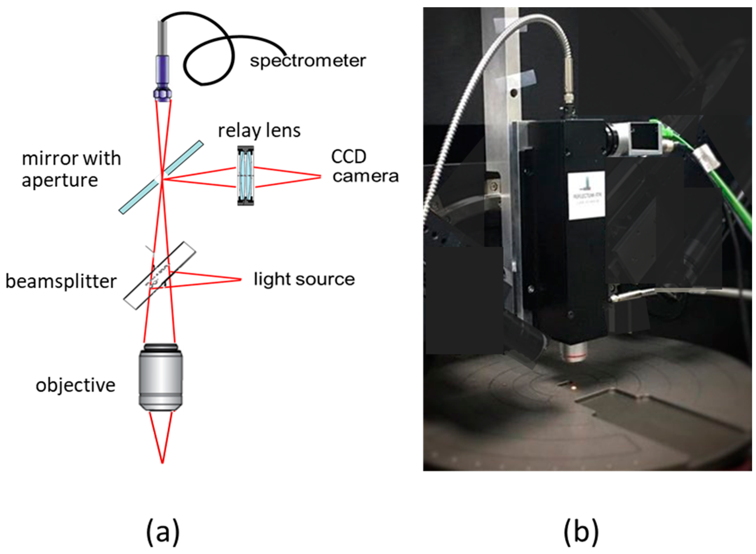
2.1. Reflectometer System Design

Figure 1 displays our in-house spectroscopic reflectometer module. This reflectometer is a nearly normal-incidence system equipped with an automated translation stage, primarily developed for measuring TSV depths and film thicknesses. We utilize a broadband tungsten halogen light source (Ocean Optics, Seminole, USA, HL-2000-HP) with an adjustable fiber connector (QP1000-2-UV-VIS+SMA 905) to maximize light throughput. A low numerical aperture (NA) of 0.1 and a low magnification (4×) microscope objective (Edmund, Barrington, IL, USA, achromatic 4×) are used to transmit nearly normal-incidence light to the high aspect ratio (HAR) TSV sample. The light waves reflected from the top and bottom of the via target structure interfere with each other and focus at an aperture before entering the spectrometer. The size of the aperture with effective areas of 50, 25, and 7.5 μm is used to control the spot size focused on the TSV sample. To enhance the amplitude of the interference spectrum, our aperture technology allows us to adjust the ratio between the illuminated area of the vias and the surface. When measuring high density via arrays, which is a common application for the spectroscopic reflectometer, we typically employ an illuminated spot size of 50 µm. However, for single via measurements, we can tailor the spot size to be slightly larger than the via diameter. A spectrometer (Ocean Optics, MAYA2000PRO) with a designed period grating and specified incident angle is used to separate the wavelengths of the captured beam. The reflectance spectrum is measured in a broadband wavelength range from 400 to 780 nm and typically exhibits regular oscillations over a large wavelength range. Spectral reflectance measurements in this range are carried out by the spectrometer with 1024 pixels. The limiting factor in this case is the pixel resolution of the spectrometer, which is approximately 0.4 nm at the upper wavelength limit of 780 nm. A viewing CCD camera (Basler, Ahrensburg, Germany, acA1600-60gm) is installed to view and identify the measurement location on the wafer.

2.2. Sample Details

Several groups of TSV samples from actual 3D interconnect processes were investigated. These TSVs have a CD (critical dimension) of 5 μm, pitches in the range of 10–45 μm, and an aspect ratio of approximately 10.

3. Theoretical Model

3.1. Basic Theoretical Model of Reflectance Spectrum

The theoretical model of the reflectance spectrum of the via structure was described in our previous publications [15,16,18]. The via structure is modeled as a film with an adjustable ratio of illuminated surface areas. The ratio of the illuminated area of the top silicon surface to the vias’ openings within the spot varies based on the sum of the total number of vias and their pitch. Let us assume the ratio coefficient α and (1 − α) represents the portion of the illuminated silicon top surface, and the total vias’ openings, respectively. E0 is the electrical field incident onto the silicon surface and the via area. The via depth is denoted as d and the wavelength as λ. The reflectance intensity I, which is the sum of the two reflected beams from the silicon surface and the via bottom surface, can be expressed as follows:
I ¯ = C o n s t α E 0 2 + ( 1 α ) E 0 2 + 2 α ( 1 α ) E 0 2 cos ( 2 π ( 2 d / λ ) )
The third term in Equation (1) indicates that the electrical field reflectance carries information about the TSV depth d. This result arises from the interference between the reflected light from the silicon top surface and the reflected light from the via bottom surface.
According to the Fresnel equation, light in air that reflects off a silicon surface will undergo a 180° shift and its electrical field reflectance will be influenced by a reflecting factor, rsi+. The simulated reflectance intensity can be calculated by multiplying the reflecting factor rsi+:
I ¯ = C o n s t α ( r S i + E 0 ) 2 + ( 1 α ) ( r S i + E 0 ) 2 + 2 α ( 1 α ) ( r S i + E 0 ) 2 cos ( 2 π ( 2 d / λ ) )

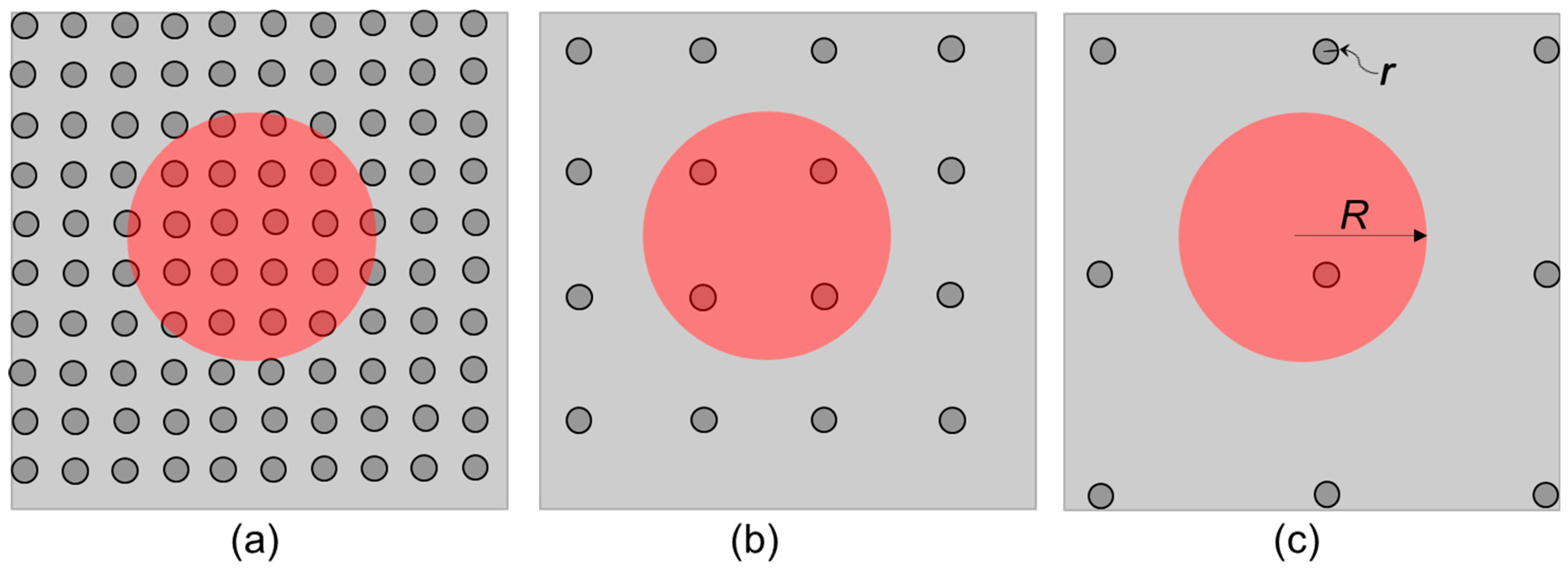
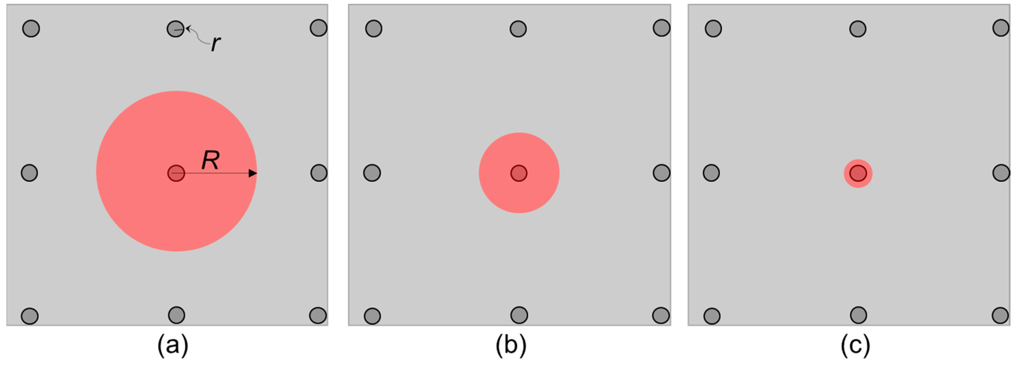
3.2. Modulation of Ratio of the Illuminated Areas

Figure 2 shows the case of an illuminated spot of 50 μm (spot radius R ≈ 25 μm), via CD of 5 μm (top via opening radius r ≈ 2.5 μm), and the pitch varies from 10, 25, to 45 μm in (a), (b), and (c), respectively. Note that only one via can be covered within the illuminated spot when the measuring vias’ pitch is 45 μm. Table 1 lists the ratio of the illuminated areas of the top silicon surface and vias’ openings to the total surface area at varying pitches.
Figure 3 shows the case of a single via measurement. Via CD is 5 μm (top via opening radius r ≈ 2.5 μm), and the illuminated spot varies from 50, 25, to 7.5 μm in (a), (b), and (c). Table 2 lists the ratio of the illuminated areas of the top silicon surface and via opening to the total surface area.

4. TSV Depth Measurement Algorithm

Evaluation of TSV depths can be accomplished using two approaches: Fast Fourier Transformation (FFT) analysis and physical model fitting. Figure 4 illustrates the measurement algorithm flow for assessing a TSV array (with a critical dimension of 3 μm and an aspect ratio of 9~10) that includes an oxide layer on top as an example. FFT analysis provides a quick and straightforward method for processing the measured reflectance spectrum and obtaining depth results, typically within 0.2 s. The model fitting for TSV depth determination involves fitting the measured reflectance spectrum data to a modified thin-film model, as described in Section 3.1. This model’s parameters include the depth of the TSV and the thickness of the top surface layer, which are adjustable. Both methods will be discussed in detail in the following two sections.

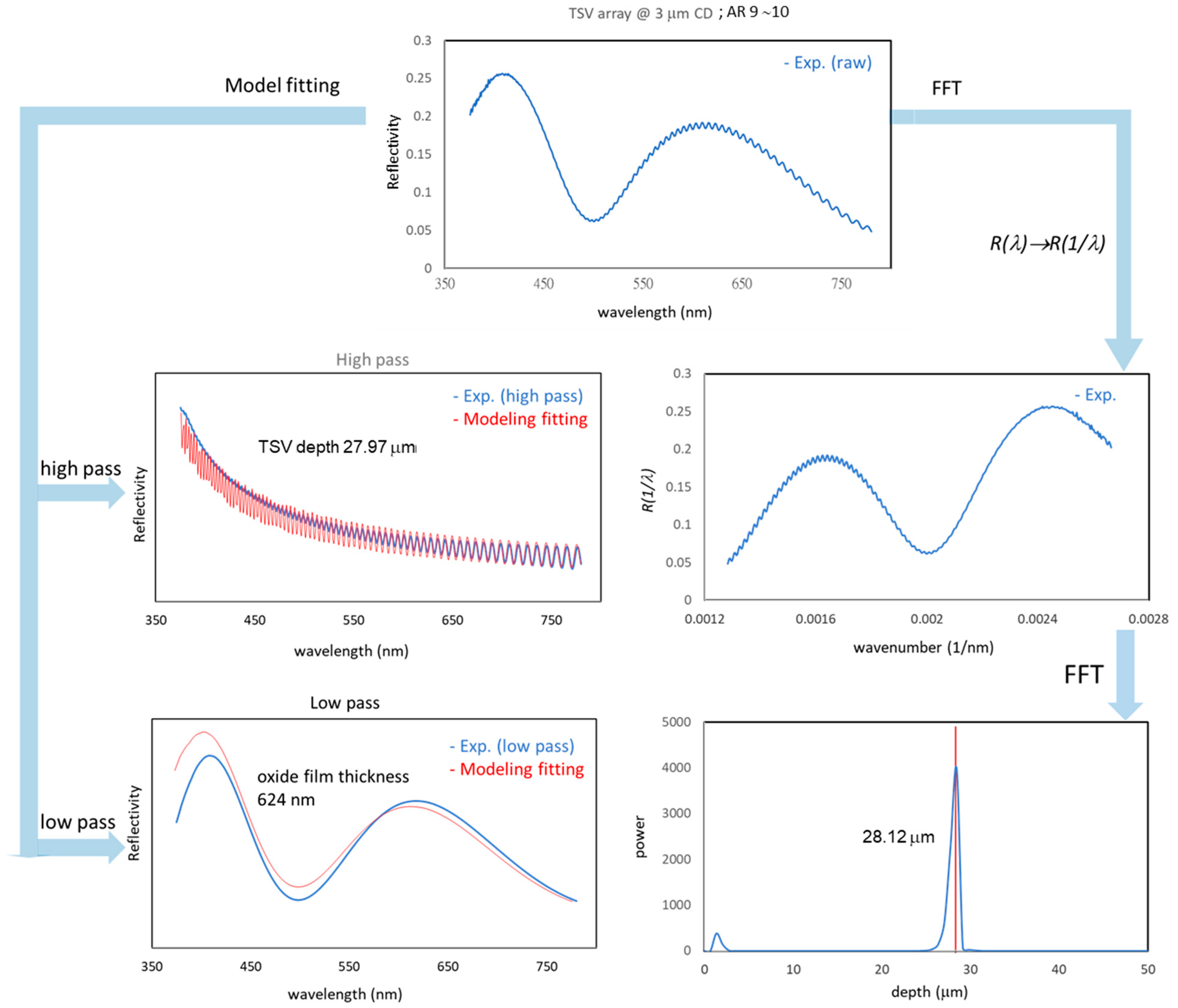
4.1. Fast Fourier Transformation (FFT)

The FFT algorithm flow is depicted in the right-hand portion of Figure 4. Initially, we convert the acquired reflectance spectrum, which is based on the wavelength (λ), into the frequency domain (1/λ). This conversion is necessary because the cosine term in Equations (1) and (2) depends on 1/λ, as does the via depth, d. To apply the FFT method for obtaining depth information, the converted reflectance spectrum needs to undergo recalibration through spline interpolation and zero-padding. This process ensures evenly spaced intervals, and the total number of sampled data points must be a power of 2 [22].
Subsequently, we implement the FFT analysis approach to determine the via depth, which in this case is measured at 28.12 μm. However, it is important to note that another FFT result appears at a depth of approximately 1–2 μm. We choose not to consider this result because it approaches the minimum resolvable depth for the applicability of the FFT. Typically, FFT analysis is limited to depths greater than around 1 μm, depending on the spectral range of the spectrometer and optical constants. In general, FFT is highly effective in handling dense oscillations and serves as an efficient method for acquiring via depth information.

4.2. Electromagnetic Model Fitting

The model fitting algorithm flow is illustrated in the left-hand part of Figure 4. The via critical dimension (CD) is approximately 3 μm, and the via pitch is around 6 μm. The illuminated areas of the top oxide surface and the via openings are roughly 80% (α) and 20% (1 − α) of the total surface area, respectively. Low and high-frequency oscillations were extracted using a spectrum processing algorithm and fitted with the modeled spectrum calculated from Equation (2). We selected a fitting metric that assesses the agreement between the number of matching oscillations and their intervals within the spectral range of 500 nm to 780 nm, comparing the measured data to the model. The fitting parameters, depth, and film thickness, which directly affects the number of modeled oscillations and their intervals, are automatically adjusted to minimize the merit function, achieving the best-fit result. It is important to note that the measured reflectance is influenced by the TSV bottom surface profile and roughness, causing exponential attenuation. The shorter the wavelength range, the stronger the attenuation. This attenuation was previously addressed in our publication [18] and is not included in the current theoretical model to save iteration time for fitting multiple parameters. Via bottom profile and roughness affect only the reflectance attenuation and do not change the density of spectral oscillations.
We achieved an excellent model fit for both high-pass and low-pass reflectance spectra, resulting in an associated via depth of 27.97 μm and an oxide thickness of 624 nm. In conclusion, the model fitting algorithm excels in providing high-resolution TSV depth determination and can measure top layer thicknesses in the tens of nanometers range. However, it is noteworthy that achieving the best-fit results may require a significant number of iterations, which can take several tens of seconds.

5. Experimental Results and Discussion

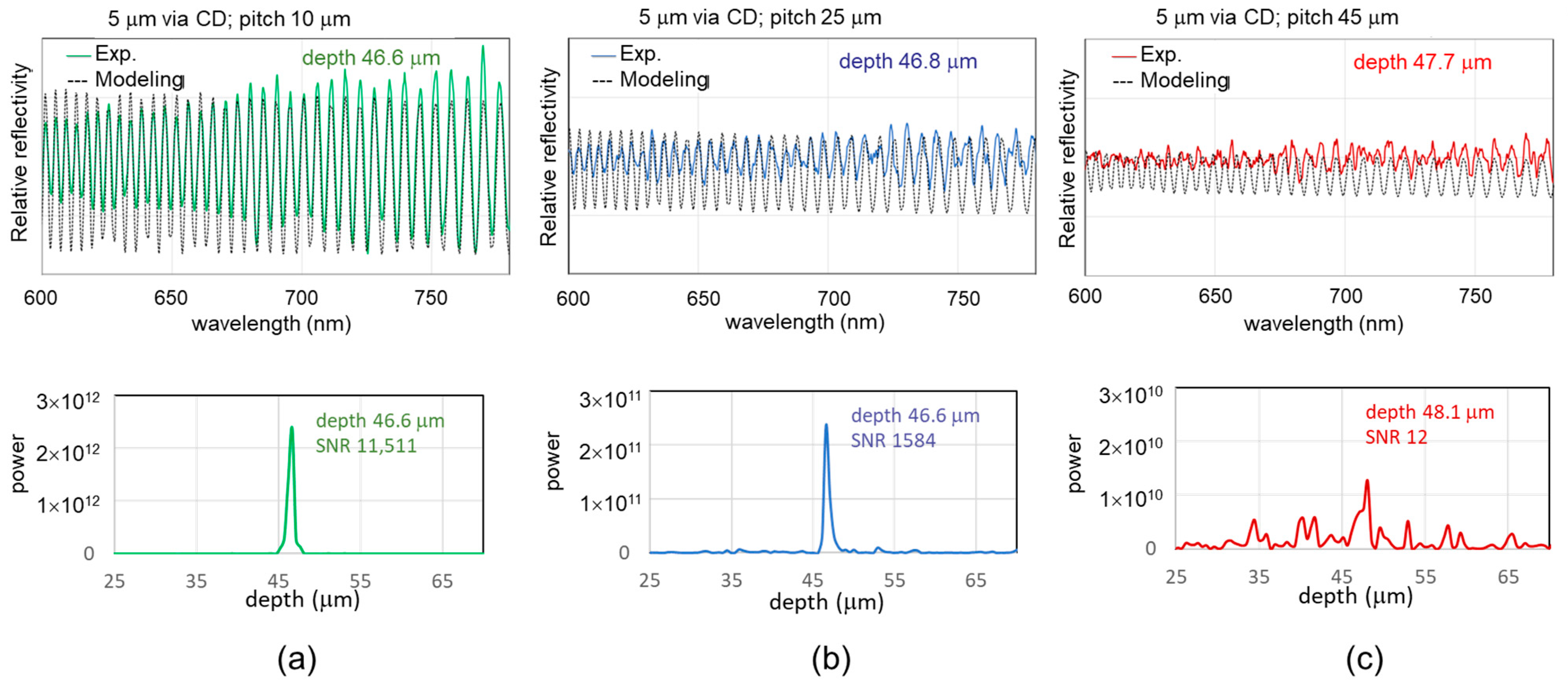
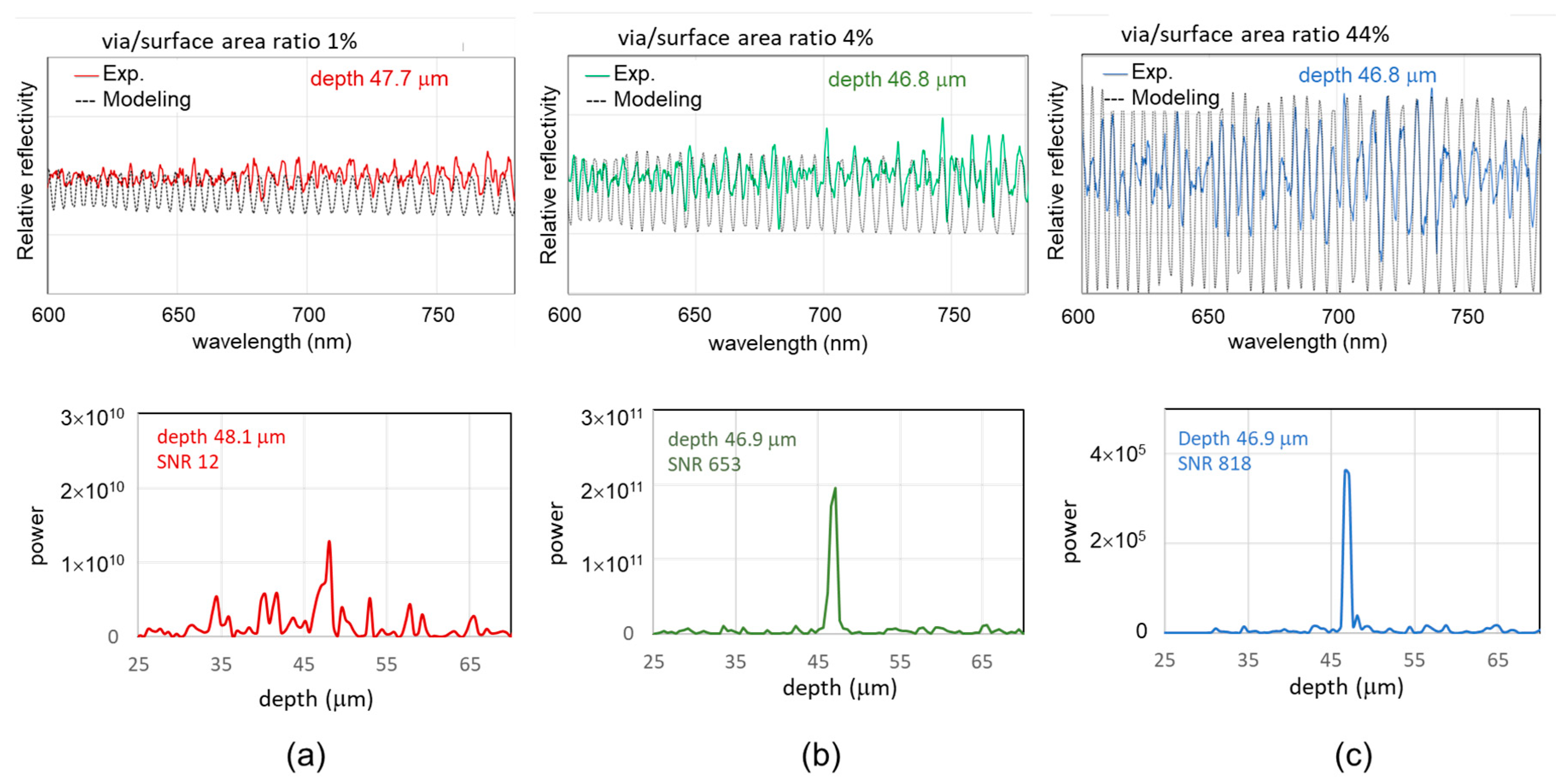
5.1. TSV Measurement Results of Varying the Ratio of Illuminated Area

Figure 5 displays the measurement results of three TSV samples with via diameters of 5 μm and pitches at 10, 25, and 45 μm. With a measuring spot size of 50 μm, the ratio of the illuminated area of the vias openings to the surface is approximately 20%, 4%, and 1%, as plotted in Figure 3. The exposure time of the spectrometer for these results was set at 100 ms with an average of 8 times. Pre-measurement setup of dark signal and reference signal were performed to reduce noise. The nominal power of the light source is 8.8 mW. The modeling fitting and FFT analysis results are presented in the upper and lower parts of Figure 5. We employed a gradient measure to analyze the zero-cross points, which reflect the number of oscillations and intervals of each oscillation. Figure 5 only depicts the fitting results in the spectral range of 600 nm to 780 nm to clearly demonstrate the level of agreement. In Figure 5a, the experimental data shown in the upper part exhibits a good fit with the modeling at a depth of 46.6 μm in terms of the number of oscillations and their intervals. The FFT result displays a distinct, sharp peak at a depth of 46.6 μm with a high signal-to-noise ratio (SNR) of 11,511. Similarly, in Figure 5b, the experimental data is well-fitted with the modeling data at 46.8 μm, and the FFT result also presents a clear power spectrum at a depth of 46.6 μm, with an SNR of 1584. However, in the case of measuring a single via, where the ratio of the illuminated area of the via to the surface drops to 1%, as shown in Figure 5c, the modeling fitting could not reach an acceptable minimum, either in terms of the number of oscillations or their intervals. Therefore, the result of a depth of 47.7 μm is not reliable. Furthermore, the FFT result exhibits a very noisy spectrum with a low SNR of only 12.

5.2. Aperture Technology Optimizing TSV Measurement

Figure 6 illustrates the measurement results of TSV samples with a via diameter of 5 μm and a pitch of 45 μm, with the illuminated spot size varying as follows: (a) 50 μm, (b) 25 μm, and (c) 7.5 μm. As the spot size varies, the ratio of the illuminated area of the vias openings to the surface changes to approximately 1%, 4%, and 44%, as plotted in Figure 4. The modeling fitting and FFT analysis results are presented in the upper and lower parts of Figure 6. In Figure 6a, we encounter the same scenario as measuring a single via, with a 1% ratio of the illuminated area of the via to the surface, as discussed in Figure 5c. The modeling fitting and FFT calculation results are not acceptable due to the low signal-to-noise ratio (SNR). Moving to Figure 6b, where the sample has a 4% ratio of the illuminated area of the via to the surface, the experimental data exhibits a reasonable fit at 46.8 μm, and the FFT calculation results in a depth of 46.9 μm with an SNR of 653. In the upper part of Figure 6c, we observe that when measuring a sample with a 44% ratio of the illuminated area of the via to the surface, the experimental data fits well with a depth of 46.8 μm, and the FFT result shows a clear peak at a depth of 46.9 μm with a high SNR of 818.
Clearly, reducing the aperture size from larger to smaller decreases the incident light intensity in the spectrometer. However, it simultaneously increases the ratio of illumination on vias to the top surface, enhancing the interference signal and FFT SNR.

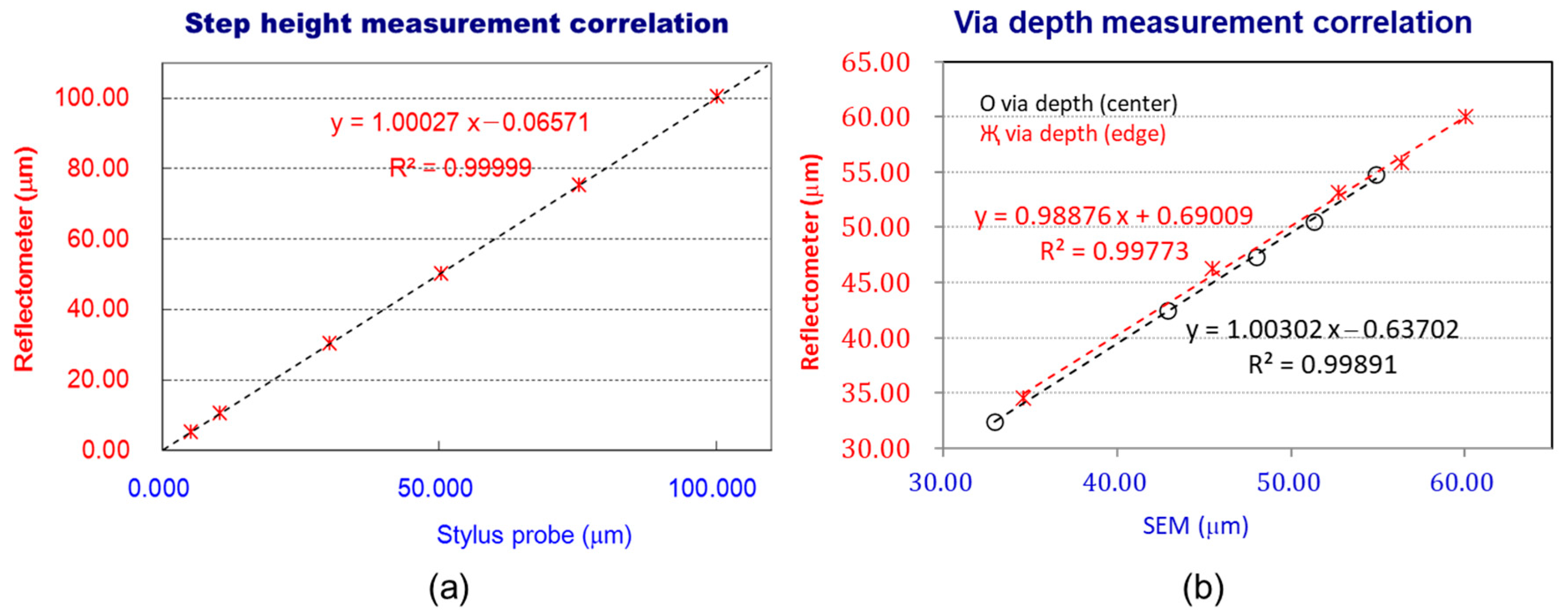
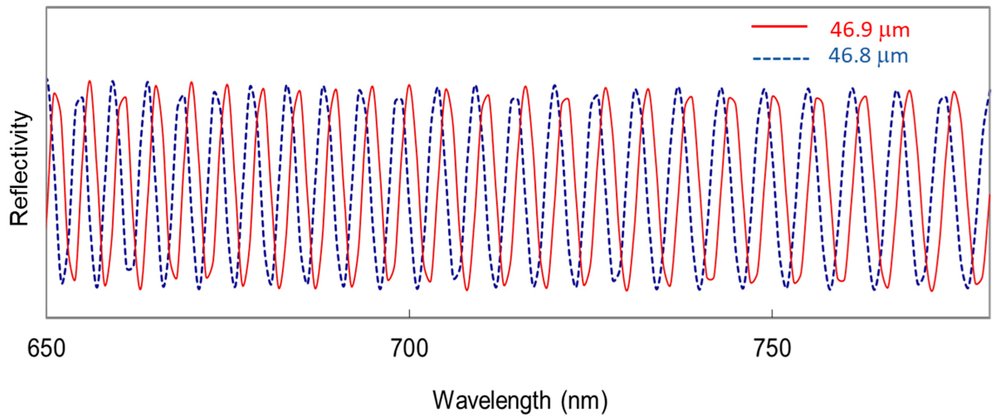
5.3. Accuracy and Resolution of Measuring TSV Depth

While there are no traceable standards for TSV depth determination, we have adopted two methods to verify the accuracy of our TSV measurements [16,18]. One approach involves comparing the results of measuring certified step heights between our reflectometer and a traceable stylus probe. These step heights serve as a relative depth reference. The second method involves establishing the correlation between TSV depths measured using cross-sectional SEM and the reflectometer within a range of several tens of micrometers. Figure 7a displays the investigation results of calibrated step heights with nominal values of 5, 10, 25, 50, and 100 μm, as measured by our reflectometer and a stylus tool. It reveals a strong linearity between the calibration data and the optical data within the entire range of step heights, with nearly zero offset in the extrapolation. The discrepancy in each individual measurement is less than 0.5%. In Figure 7b, we present the measurement correlation between cross-sectional SEM and the reflectometer in the TSV depth range from 30 to 60 μm. The results demonstrate a robust linearity, and the discrepancies within the range of 30 to 60 μm are within submicron limits.
The resolution of TSV depth determination primarily relies on the spectrometer’s entrance slit and the density of the diffraction grating. The entrance slit limits the amount of light that can be collected by the spectrometer, while the grating spacing determines the angular range of diffraction versus wavelength. In general, smaller slit widths and grating spacings result in greater resolution, but they may require some sacrifice in signal intensity. Commercial spectrometers typically strike a balance between spectral resolution and sensitivity. Figure 8 presents the theoretical modeling of the reflectance spectrum for via depths of 46.8 μm and 46.9 μm. The spectra for the two via depths are well separated from each other. Ideally, the TSV depth measurement resolution should fall within the range of tens of nanometers. While acknowledging that some noise may introduce challenges in accurately discerning true peaks, we can conclude that the resolution for TSV depth determination through model regression analysis is ≤0.1 μm.
If the spectral range of the spectrometer is given by λmin and λmax, the first complete oscillation in the spectrum of a TSV sample with refractive index, nair = 1, can be considered if one maximum appears at λmin and the second maximum appear at λmax as derived in Equation (3). Note that FFT analysis requires at least one full oscillation in the spectrum, and it delivers the depth result through a discrete integer number m multiplying by Δd. The resolution Δd is given by the smallest step spectral range of our spectrometer’s range, which is 0.4 μm, covering the range from 400 nm to 780 nm.
Δ d = 1 2 n a i r 1 λ m i n 1 λ m a x

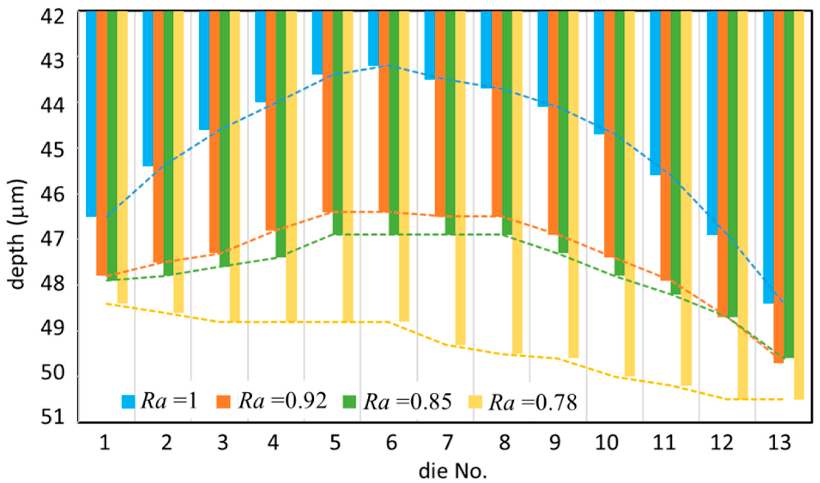
5.4. Uniformity of High Aspect Ratio TSV Etch

Many factors affect etch performance, as discussed in previous studies [19,23]. Two main issues, temperature control and chemistry control, were the focus of advanced tools to improve wafer etching uniformity. Recently developed etching tools provide multiple independent heaters to control micro-zone temperatures across the wafer, which significantly impacts etched depth uniformity. Additionally, tuning various parameters to control the chemistry across the wafer has been addressed to achieve better uniformity. This has been achieved by introducing tuning gases at separate locations from the main reactant gas.
Our current reactive ion etch (RIE) system, which was developed in the early 2000s, does not allow for adjustable settings of the chuck temperature or the percentage of chemistry gas injection. However, we carefully tune the ratio of the R.F. current applied to the outer and inner coils, which is a tunable parameter to control plasma ion density over the wafer’s outer and inner zones, thereby achieving better uniformity. In Figure 9, we present the variation in the etched depths of TSV arrays with a nominal 5 μm critical dimension and an aspect ratio of 10. We measured die-to-die variations as a function of position across a 300 mm diameter test wafer. The uniformity of via depth is defined as
U n i f o r m i t y % = d e p t h m a x d e p t h m i n 2 d e p t h a v e 100 %
Ra represents the current ratio applied to the outer/inner coil of the dual tunable plasma sources in the RIE process chamber. Initially, Ra was set at 1, which meant an equal current was applied to both the outer and inner coils to generate etching plasma covering the entire wafer. However, the uniformity of etched TSV depth, measured from the bottom wafer edge across the center to the upper wafer edge, was surprisingly poor at 5.79%. The minimum etch depth was observed in the center area, and it became deeper as we moved toward the wafer edges. This phenomenon was most likely attributable to chemical concentration gradients across the wafer. These gradients encompassed variations in reactant consumption, by product emission rates, and discrepancies in temperature between the center and the edges of the wafer.
To reduce the depth variations, we adjusted Ra to several different settings: 0.92, 0.85, and 0.78 in subsequent experiments. These adjustments increased the ion density in the center wafer zone to some extent. Table 3 lists the die-to-die via depth measurement results at different Ra settings. The uniformities improved significantly, from 5.79% to 2.13%, as Ra was tuned from 1 to 0.78. Significantly, the minimum etch depth was no longer observed in the center die when Ra was set to 0.78. This indicates a substantial reduction in the influence of the chemical concentration gradient between the center and wafer edges. It is worth mentioning that for all four Ra settings the maximum etch depths were consistently observed in the top edge die (no. 13 die). We believe this was caused by the turbomolecular pump located on the side of the chamber, corresponding to the top side of the wafer. This led to side-to-side depth variations due to the convective flow of reactants and byproducts laterally across the wafer.

6. Summary

This paper presents an in-house designed spectroscopic reflectometer equipped with an adjustable aperture capable of measuring an average number of TSVs, an individual TSV, or other specific periodic arrays of TSVs. The fact that our module can perform non-destructive and extremely fast via depth measurements opens up the possibility of mapping via depth data within a die and across the entire wafer. It can also be used to optimize etch-depth uniformity based on quick reflectometer feedback data obtained during the reactive ion etch (RIE) process.
Future work will involve exploring measurement algorithms by combining modeling fitting and FFT methods for more complicated samples, providing rapid solutions for high aspect ratio TSV depths and thicknesses of multiple material layers on top of the TSV structure.

Author Contributions

Conceptualization, Y.-S.K.; methodology, C.-H.C.; software, C.-W.L.; formal analysis, C.-K.L.; validation, W.-Q.C. and P.-W.C. writing—original draft preparation, Y.-S.K.; writing—review and editing, Y.-S.K.; All authors have read and agreed to the published version of the manuscript.

Funding

This work was funded by MOEA (Ministry of Economic Affairs) grant number 111-EC-17-D-11-1801.

Data Availability Statement

The data presented in this study are available on request from the corresponding author.

Acknowledgments

The authors thank Mike Chang and Ying-Tzu Hung at the EOSL/ITRI (Electronic and Optoelectronic System Research Laboratories/Industrial Technology Research Institute) for their great help on manufacturing HAR TSV wafers.

Conflicts of Interest

The authors declare no conflict of interest.

References

  1. IRDS Metrology 2023. Available online: https://irds.ieee.org/images/files/pdf/2023/2023IRDS_MET.pdf (accessed on 15 October 2023).
  2. Wang, J.; Duan, F.; Lv, Z.; Chen, S.; Yang, X.; Chen, H.; Liu, J. A Short Review of Through-Silicon via (TSV) Interconnects: Metrology and Analysis. Appl. Sci. 2023, 13, 8301. [Google Scholar] [CrossRef]
  3. Huang, P.K.; Lu, C.Y.; Wei, W.H.; Chiu, C.; Ting, K.C.; Hu, C.; Tsai, C.H.; Hou, S.Y.; Chiou, W.C.; Wang, C.T.; et al. Wafer Level System Integration of the Fifth Generation CoWoS®-S with High Performance Si Interposer at 2500 mm2. In Proceedings of the Electronic Components and Technology Conference (ECTC), San Diego, CA, USA, 1 June–4 July 2021; pp. 101–104. [Google Scholar] [CrossRef]
  4. Banijamali, B.; Lee, T.; Liu, H.; Ramalingam, S.; Barber, I.; Chang, J.; Kim, M.; Yip, L. Reliability evaluation of an extreme TSV interposer and interconnects for the 20 nm technology CoWoS IC package. In Proceedings of the Electronic Components and Technology Conference (ECTC), San Diego, CA, USA, 26–29 May 2015; pp. 276–280. [Google Scholar] [CrossRef]
  5. Zhang, X.; Lin, J.K.; Wickramanayaka, S.; Zhang, S.; Weerasekera, R.; Dutta, R.; Chang, K.; Chui, K.; Li, H.; Ho, D.; et al. Heterogeneous 2.5D integration on through silicon interposer. Appl. Phys. Rev. 2015, 2, 021308. [Google Scholar] [CrossRef]
  6. Semi Draft Document 5410. Guide for Metrology Techniques to be used in Measurement of Geometrical Parameters of Through-Silicon Vias (TSVs) in 3DS-IC Structures; Semiconductor Equipment and Materials International: San Jose, CA, USA, 2013. [Google Scholar]
  7. de Groot, P.; de Lega, X.C. Valve cone measurement using white light interference microscopy in a spherical measurement geometry. Opt. Eng. 2003, 42, 1232. [Google Scholar] [CrossRef]
  8. Belk, J.H.; Hulsey, D.E. Non-Contact Hole Depth Gage. U.S. Patent 2003/0107728 A1, 12 June 2003. [Google Scholar]
  9. Grimberg, H.; Bloomhill, M.; Koren, S. Depth Measurement of Narrow Holes. U.S. Patent 2011/0184694 A1, 28 July 2011. [Google Scholar]
  10. Teh, W.H.; Caramto, R.; Qureshi, J.; Arkalgud, S.; O’Brien, M.; Gilday, T.; Maekawa, K.; Saito, T.; Maruyama, K.; Chidambaram, T.; et al. A route towards production-worthy 5 μm × 25 μm and 1 μm × 20 μm non-Bosch through-silicon-via (TSV) etch, TSV metrology, and TSV integration. In Proceedings of the IEEE International Conference on 3D System Integration, San Francisco, CA, USA, 28–30 September 2009. [Google Scholar]
  11. Knowles, M. Optical metrology for TSV process control. In Proceedings of the 3D Interconnect Metrology at the SEMATECH Workshop during SEMICON West, San Francisco, CA, USA, 14–16 July 2009. [Google Scholar]
  12. Timoney, P.; Fisher, D.; Ko, Y.; Vaid, A.; Thangaraju, S.; Smith, D.; Kamineni, H.; Zhang, D.; Alapati, R.; Kim, W.; et al. New Interferometric Measurement Technique for Small Diameter TSV. In Proceedings of the 25th Annual SEMI Advanced Semiconductor Manufacturing Conference (ASMC 2014), Saratoga Springs, NY, USA, 19–21 May 2014; pp. 37–41. [Google Scholar] [CrossRef]
  13. Marx, D.; Grant, D.; Dudley, R.; Rudack, A.; Teh, W.H. Wafer Thickness Sensor (WTS) for Etched Depth Measurement of TSV. In Proceedings of the International Wafer-Level Packaging Conference (IWLPC), Santa Clara, CA, USA, 27–30 October 2009. [Google Scholar]
  14. Teh, W.H.; Marx, D.; Grant, D.; Dudley, R. Backside Infrared Interferometric Patterned Wafer Thickness Sensing for Through-Silicon-Via (TSV) Etch Metrology. IEEE Trans. Semicond. Manuf. 2010, 23, 419–422. [Google Scholar] [CrossRef]
  15. Ku, Y.S.; Yang, F.S. Reflectometer-based metrology for high-aspect ratio via measurement. Opt. Express 2010, 18, 7269–7280. [Google Scholar] [CrossRef] [PubMed]
  16. Ku, Y.S.; Huang, K.C.; Hsu, W. Characterization of high density through silicon vias with spectral reflectometry. Opt. Express 2011, 19, 5993–6006. [Google Scholar] [CrossRef] [PubMed]
  17. Fursenko, O.; Bauer, J.; Marschmeyer, S. In-line through silicon vias etching depths inspection by spectroscopic reflectometry. Microelectron. Eng. 2014, 122, 25–28. [Google Scholar] [CrossRef]
  18. Ku, Y.S. Spectral reflectometry for metrology of three-dimensional through-silicon vias. J. Micro/Nanolith. MEMS MOEMS 2014, 13, 011209. [Google Scholar] [CrossRef]
  19. Wu, B.; Kumar, A.; Pamarthy, S. High aspect ratio silicon etch: A review. J. Appl. Phys. 2010, 108, 051101. [Google Scholar] [CrossRef]
  20. Singh, H.; Rusu, C.; Vahedi, V. Etch challenges for 3-D integration. In Proceedings of the 3rd Workshop on Plasma Etch and Strip in Microelectronics, Grenoble, France, 4–5 March 2010. [Google Scholar]
  21. Puech, M.; Thevenoud, J.M.; Gruffat, J.M.; Launay, N.; Arnal, N.; Godinat, P. Fabrication of 3D packaging TSV using DRIE. In Proceedings of the Symposium on Design, Test, Integration and Packaging of MEMS/MOEMS, Nice, France, 9–11 April 2008. [Google Scholar]
  22. Quinten, M. A Practical Guide to Optical Metrology for Thin Films; Wiley-VCH Verlag GmbH & Co. KGaA: Weinheim, Germany, 2012; ISBN 978-3-527-66434-4. [Google Scholar]
  23. Chen, L.; Wang, Q.; Griesmann, U. Plasma etching uniformity control for making large and thick dual-focus zone plates. Microelectron. Eng. 2011, 88, 2466–2469. [Google Scholar] [CrossRef]
Figure 1. TSV measurement module: (a) schematic design, (b) photo.
Metrology 03 00022 g001
Figure 2. Illustration of an illuminated spot of 50 μm (red area), via CD of 5 μm (dark gray circle), and the pitch varies from (a) 10 μm, (b) 25 μm, and (c) 45 μm, respectively.
Metrology 03 00022 g002
Figure 3. Illustration of an illuminated spot (red) of (a) 50 μm, (b) 25 μm, and (c) 7.5 μm, respectively. Via CD is 5 μm (dark gray), and the pitch is 45 μm.
Metrology 03 00022 g003
Figure 4. The algorithm flow for TSV depth measurement. The FFT and modeling fitting analysis flow is illustrated on the right-hand side and left-hand side, respectively.
Metrology 03 00022 g004
Figure 5. Measurement results of TSV samples with via diameter of 5 μm, pitches at (a) 10, (b) 25, and (c) 45 μm. The measuring spot size is 50 μm.
Metrology 03 00022 g005
Figure 6. Measurement results of TSV samples with via diameter of 5 μm, pitches of 45 μm, spot size varying at (a) 7.5 μm, (b) 25 μm, and (c) 50 μm, respectively.
Metrology 03 00022 g006
Figure 7. (a) Comparison of reflectometer measuring results with certified values (nominal step heights are 5, 10, 30, 50, 75, and 100 μm). (b) Comparison of measurements between SEM instrument and reflectometer while measuring via depths from 30 to 60 μm [18].
Metrology 03 00022 g007
Figure 8. Theoretical modeling of reflectance spectrum for via depth 46.8 and 46.9 μm. The spectrum for via depth 46.8 μm is well separated from the one for 46.9 μm.
Metrology 03 00022 g008
Figure 9. Etched depths of TSV arrays of nominal 5 μm CD, aspect ratio 10 with the measured die-to-die as a function of position across a 300 mm diameter test wafer.
Metrology 03 00022 g009
Table 1. Ratio of illuminated areas (50 μm spot; 5 μm via CD).
Pitch
(50 μm Spot; 5 μm Via Top CD)
10 µm25 µm45 µm
1 − α
ratio of illuminated area (via)
20%4%1%
α
ratio of illuminated area (silicon surface)
80%96%99%
Table 2. Ratio of illuminated areas (5 μm via CD; 45 μm pitch).
Spot Size
(5 μm Via Top CD)
50 μm
Pitch 45 µm
25 μm
Pitch 45 µm
7.5 μm
Pitch 45 µm
1 − α: ratio of illuminated area (via)1%4%44%
α: ratio of illuminated area (silicon surface)99%96%56%
Table 3. Die-to-die TSV etch uniformity.
Ra\Die no. Depth (μm)12345678910111213Ave.Uniformity (%)
146.545.444.644.043.443.243.743.744.144.745.646.948.444.925.79
0.9248.647.547.346.846.446.446.546.546.947.447.948.749.747.323.48
0.8547.947.847.447.446.946.946.946.947.347.848.248.749.647.682.83
0.7848.448.648.848.848.848.849.349.549.650.050.250.550.549.372.13
Disclaimer/Publisher’s Note: The statements, opinions and data contained in all publications are solely those of the individual author(s) and contributor(s) and not of MDPI and/or the editor(s). MDPI and/or the editor(s) disclaim responsibility for any injury to people or property resulting from any ideas, methods, instructions or products referred to in the content.

