Article

UV Nanoimprint Lithography—Impact of Coating Techniques on Pattern Quality

EV Group, DI Erich Thallner Str. 1, 4782 St. Florian am Inn, Austria
*
Author to whom correspondence should be addressed.
Nanomanufacturing 2024, 4(1), 69-80; https://doi.org/10.3390/nanomanufacturing4010005
Submission received: 7 December 2023 / Revised: 9 January 2024 / Accepted: 8 February 2024 / Published: 14 March 2024
(This article belongs to the Special Issue Nanoimprinting and Sustainability)

Abstract

:
In this work, three different coating techniques are compared and their applicability for ultraviolet nanoimprint lithography (UV-NIL) is investigated. As UV-NIL is considered a suitable volume manufacturing production solution for various emerging applications, it is mandatory to consider environmental aspects such as operational energy use and material consumption as well as waste management. In this paper, spin coating, spray coating, and inkjet coating are used to coat both a high refractive index resin (n = 1.9) and a filler-free resin (n = 1.5), respectively. Variable Angle Spectroscopy Ellipsometry (VASE) was used to analyze the influence of different process parameters on the resin thickness as well as to compare the refractive index achieved from each coating technology. Finally, the applicability of the different coating methods for UV-NIL was investigated by imprinting the resin layers with different test structures. For the final imprints, the resolution, the surface roughness, and the pattern fidelity over 25 imprints was assessed using AFM. Finally, a comparison of the resin consumption and the process time was performed for each coating method.

1. Introduction

In recent years, ultraviolet nanoimprint lithography (UV-NIL) has emerged as an attractive patterning technique and is nowadays recommended as a suitable volume manufacturing production solution for applications in wafer level optics [1], augmented reality [2], and biomedical diagnostics [3]. The continuous development of materials, equipment, and process technology broadened the field of applications and confirmed UV-NIL as a very flexible and efficient technology applicable to fabricate a large variety of 3D pattern sizes with various shapes [4,5]. Nowadays, UV-NIL is the method of choice for various emerging applications due to the maturity of this scalable technology and its compatibility with standard semiconductor manufacturing environment [6].
For a high-volume suitable replication technique, it is mandatory to consider environmental aspects such as operational energy use and material consumption as well as waste management. Typically, UV-NIL imprints are already fully crosslinked after several seconds when exposed using a 400 mW LED light source (365 nm), which is quite a low power compared to the ones used by lithography techniques such as deep UV (DUV) and extreme UV (EUV) [7]. More importantly, the impact of material consumption generated by the coating technique can be considered as a major factor to reduce the costs and the CO2 footprint of products fabricated with UV-NIL.
Spin coating, as shown in Figure 1a, is the most established method for depositing a UV-NIL resin film on a substrate. The spin coating process starts with dispensing the resin solution on the substrate surface. The wafer is spun subsequently at high speed to homogenize the layers. The final film thickness is controlled by the spinning speed, the surface tension, and the viscosity of the resin precursor [8]. However, the material use efficiency of spin coating technique is very low: generally, about 95–98% of the material is spun off and disposed of during the process, while only 2–5% of the material remains on the substrate for use after spin-off [8]. An alternative coating technique with reduced resin consumption is shown in Figure 1b: spray coating is a promising technique for depositing thin and homogenous layers on substrates with no limitation on shape, size, and surface topography [9,10]. During the coating process, the wafer is held static while an ultrasonic spray nozzle is moving with a defined speed profile across the substrate. The film thickness is determined by the viscosity of the resin, the type, and the speed of the spray nozzle as well as the dispense rate. Another static coating technique enabling low resin consumption is the inkjet coating, shown in Figure 1c. Inkjet coating is utilizing single drops of resist allowing for precise volume control and eliminates the typical resist waste encountered with spin coating [11,12,13]. Droplets with defined volume of material are placed on predefined positions, which enable the achievement of highly customized coatings adjusted to the layout of a specific NIL stamp. The film thickness is defined by the viscosity of the resin, the droplet size, and the placement density.
This work aims to make a comparison of the different coating techniques and their impact on the imprint results. Experimental results using augmented reality typical pattern geometries and the assessment of the required resin consumption will be presented.

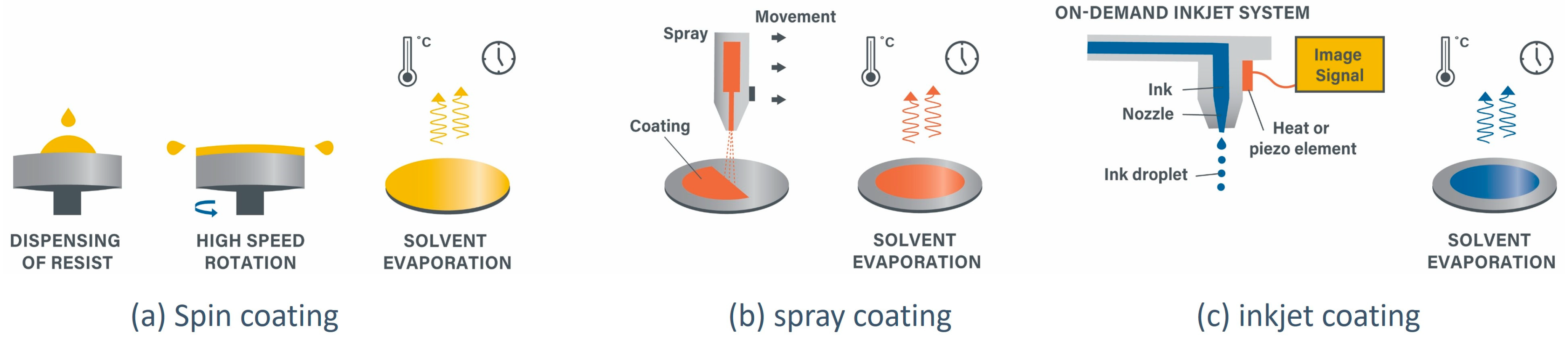
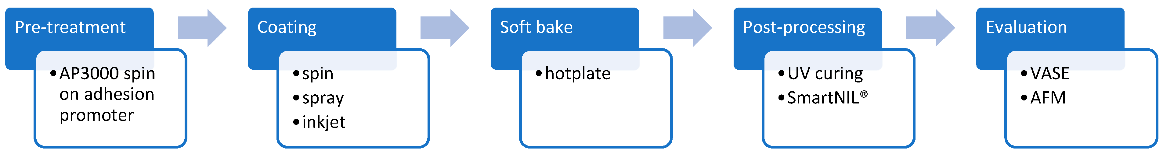
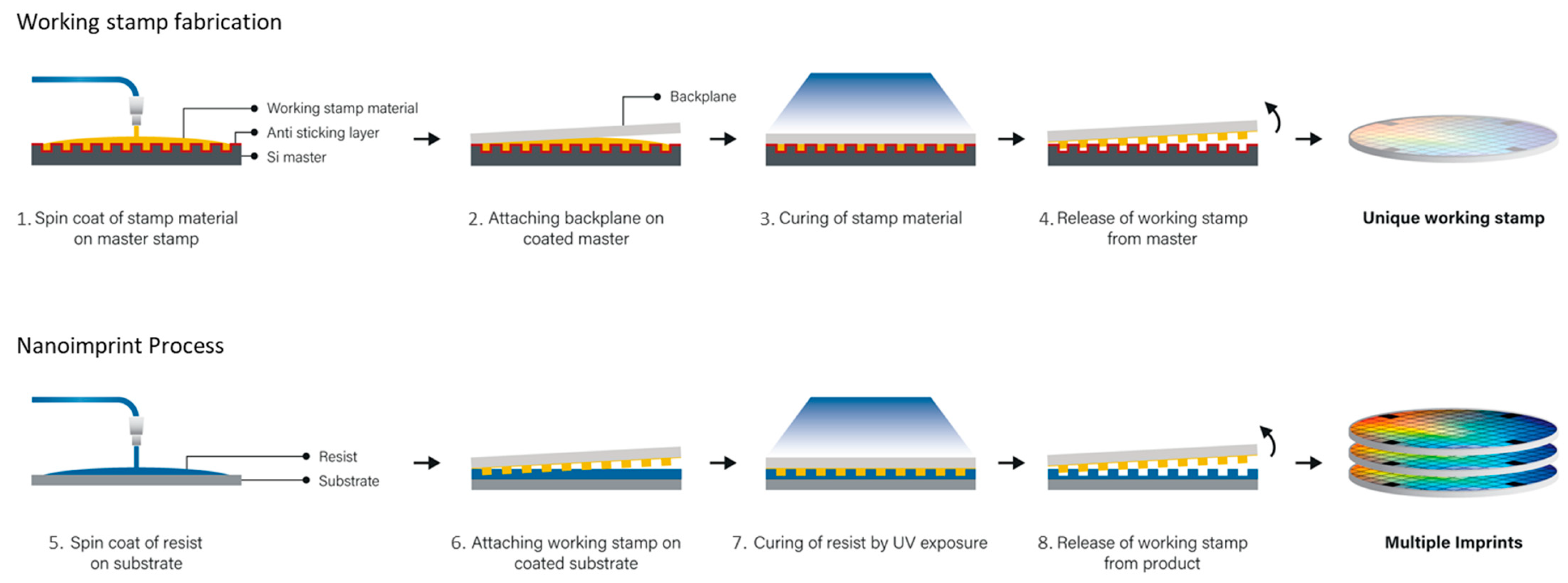
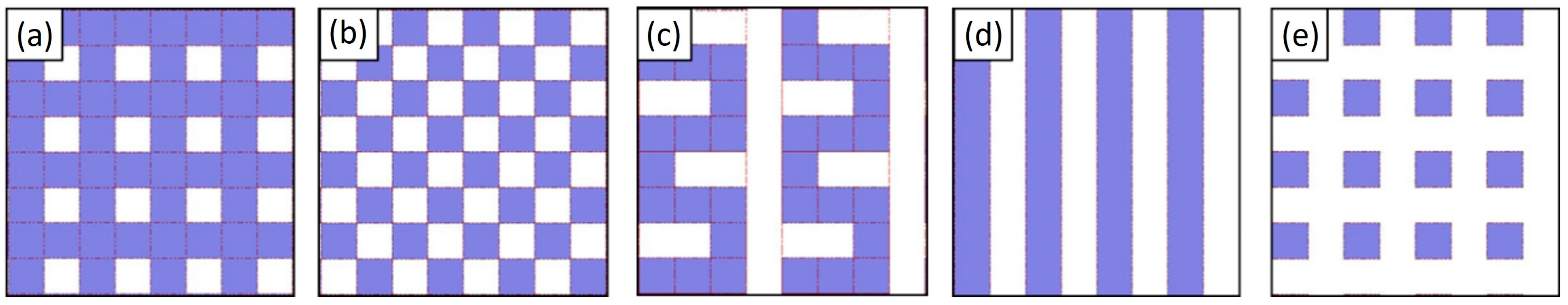
2. Materials and Methods

For the study of the spin- and spray-coating process, EVG 100® series coating equipment was used as this system can accommodate both process flows. Inkjet coating tests have been performed on a ImageXpert system equipped with a Xaar print head. In order to allow for a high degree of freedom in terms of materials choice to address the desired range in terms of viscosity and in refractive index, a syringe-based dispense method was employed. A NIL resin without fillers (n = 1.5; EVG NIL UV/A) has been investigated as well as a high refractive index resin containing TiO2 nanoparticles (n = 1.9; INKRON). Single-side polished, 200 mm-diameter, (100) orientation silicon wafers prepared with an adhesion promoter (AP3000, Rohm and Haas Electronic Materials) were used as substrates for all tests. Thin resin layers (typical for NIL in the range of 100–200 nm) were processed in a single coating step using precise dispensing. When using spin coating to achieve a specific resin layer thickness, the viscosity of the resin and the spinner speed are the most important parameters. For spray coating, the solvent content of the resin, the speed of the nozzle moving across the substrate, and the dispense rate define the final layer thickness. The resin thickness of an inkjet-coated layer is, like spray coating, defined by the solvent content, the dispense rate (drop size, number of droplets), and the speed profile of the stage. In Figure 2, the process flow is illustrated, and in Table 1, the investigated parameters are listed: for spin coating the spinner speed, for spray coating the dispense rate and for inkjet coating the droplet size. After each coating, the solvent was removed by a soft bake process performed on an EVG 105® hotplate. The soft bake temperature and duration varied depending on the resin type and solvent content between 80 °C and 120 °C for either 60 s or 90 s.
The resin layers have been characterized after coating with respect to layer thickness and uniformity using Variable Angle Spectroscopic Ellipsometry (VASE). For this purpose, a Woollam M-2000 Ellipsometer with rotating compensator was used, working in a wide spectral range (190–1687 nm). The ellipsometry measurements were performed at three different angles of incidence (60°, 65°, and 70°) in 49 sampling locations using an automated stage and the data were modelled using the CompleteEASE software (Version 6.72). To compare the effect of the coating techniques on the imprintability of the coated layer, an EVG 7200® imprint system was used to perform the SmartNIL™ process. The complete wafer level SmartNIL™ process flow shown in Figure 3 consists of the fabrication of the working stamp (steps 1–4) and the actual imprint process on the substrate (steps 5–8) [5,14,15]. Typically, the master stamp providing the actual topography of the desired structures for the replication is prepared on silicon using e-beam lithography and subsequent etching. The replication process (imprinting on the layer coated on the substrate) is using a working stamp which is produced based on the master stamp. To ensure a defect-free working stamp fabrication, the master stamp must be coated with an anti-sticking layer (ASL) to minimize the surface energy and allow for good detachment at the end of the imprinting process. The working stamp fabrication starts with dispensing the material by spin coating on the master template and mounting a flexible backplane in the EVG 7200® system. Secondly, the coated master stamp is contacted with the backplane, the working stamp material is cured and thus the negative of the master stamp surface topography is replicated in the working stamp polymer. Finally, the working stamp can be demolded after solidification and is then used for the actual nanoimprint process. With respect to restriction under consideration (ECHA), the materials used for all investigations did not contain Polyfluorinated Acrylate (PFA) substances.
The evaluation of the imprint process was performed on test structures with a geometry typically used for waveguides (Figure 4; 400 nm line/space template) and a template with different geometric layouts and resolution down to 50 nm (Figure 5). The comparison of the imprintability of the differently coated resin layers has been assessed measuring the imprinted structures using a Bruker Fast Scan Dimension Atomic Force Microscope (AFM), equipped with FastScan C needles with 5 nm tip radius and working in scan assist mode (similar to tapping mode). Typical scan fields were 10 × 10 µm2 or 1 × 5 µm2.

3. Results

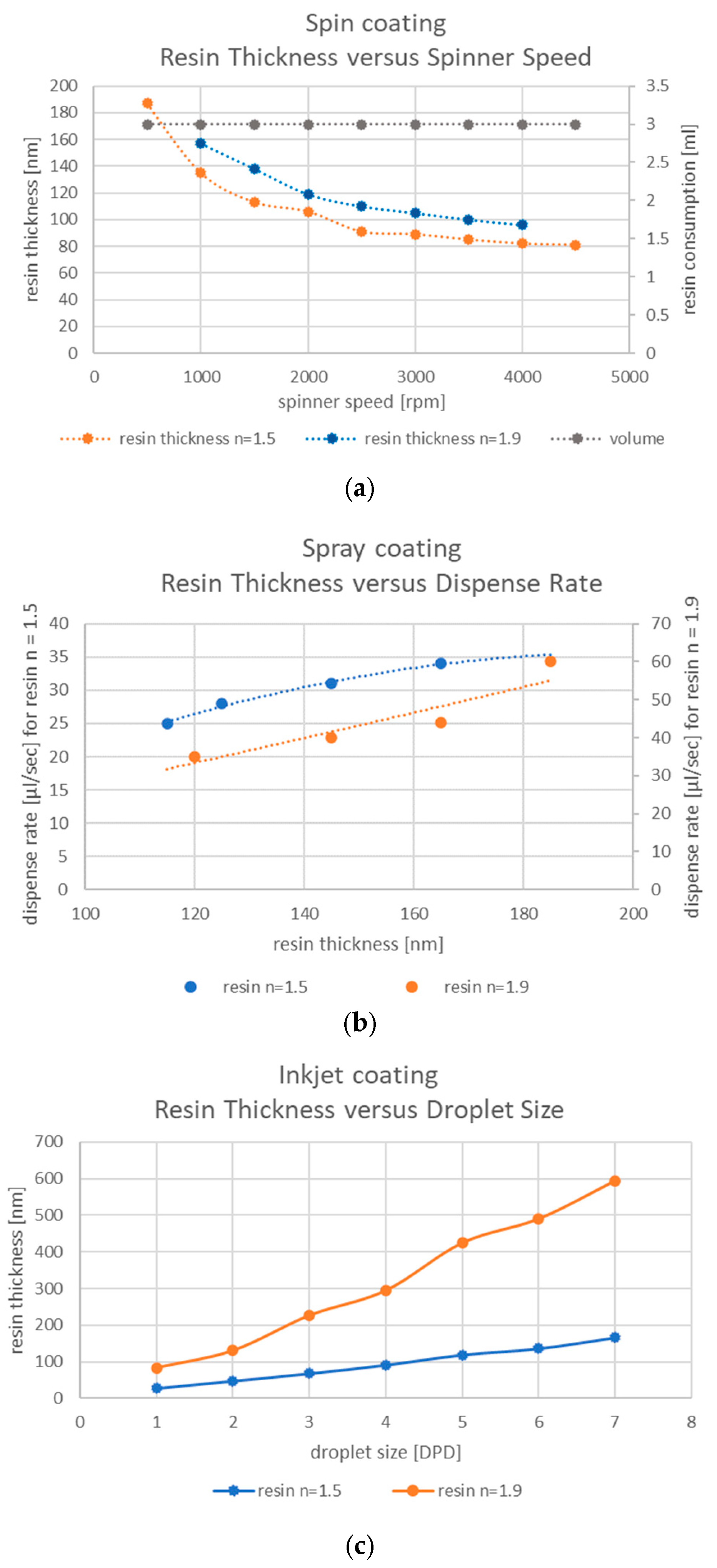
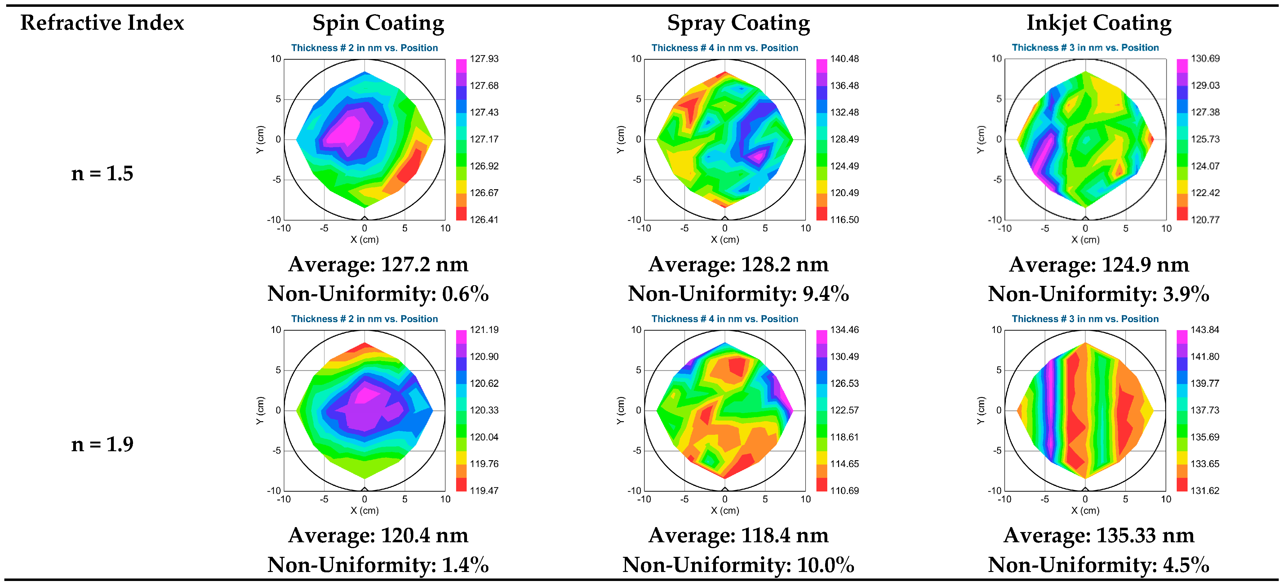
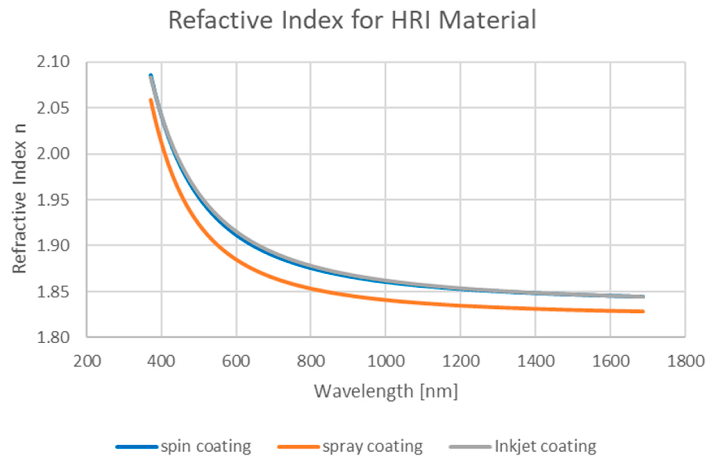
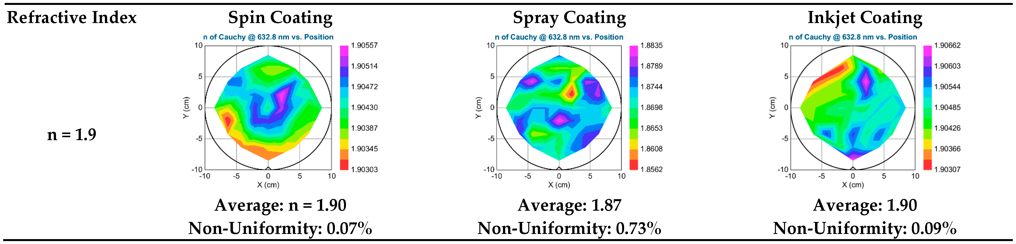
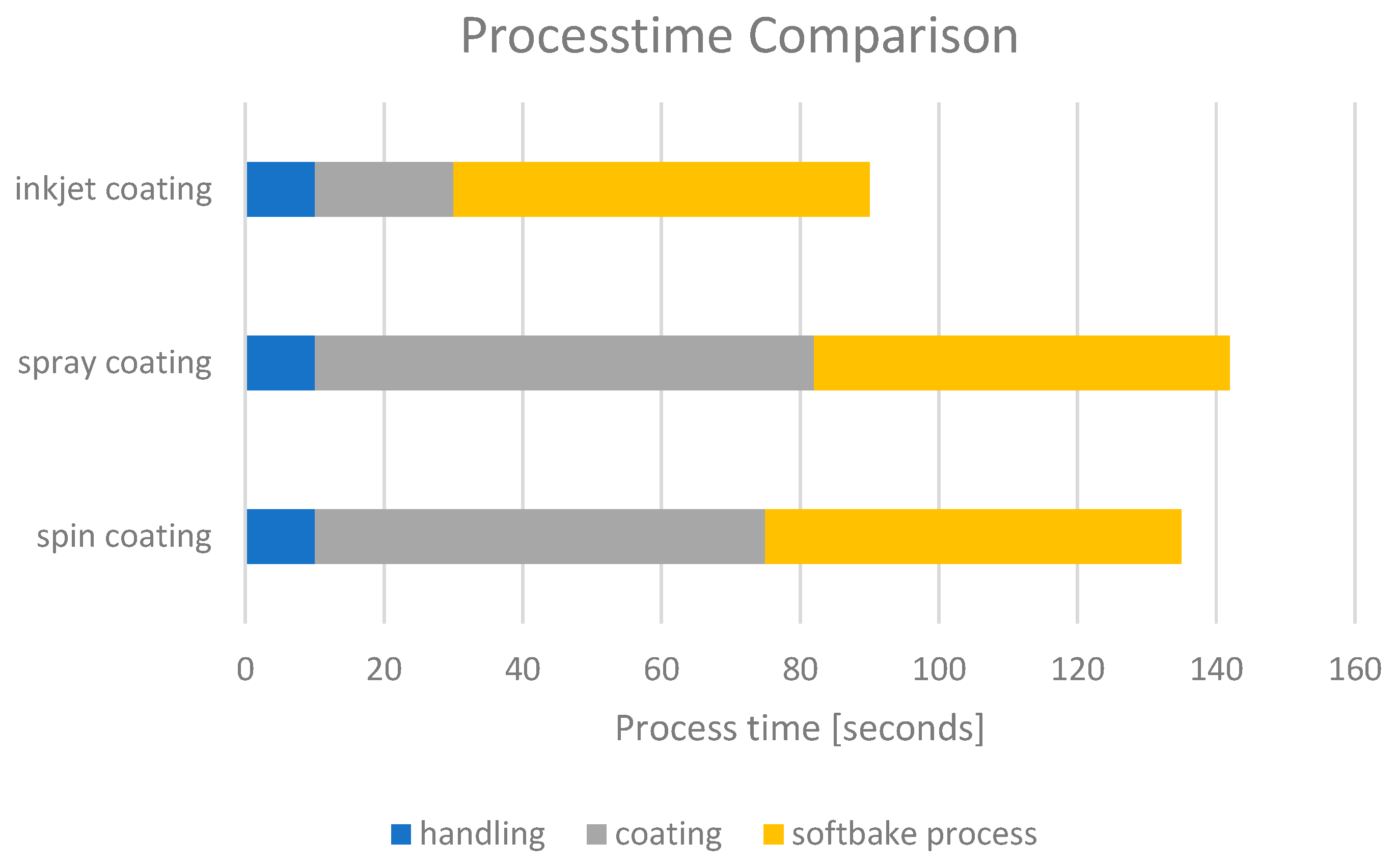
3.1. Coating Performance

For the imprint processes, the layer thickness and uniformity control is often crucial to achieve the desired imprint quality. In particular, this is required if the residual layer thickness has to be minimized in order to facilitate subsequent etching processes using the imprinted features as an etching mask. If the imprint is already the final device, typically functional resins like high refractive index materials are used, and a uniform layer thickness is crucial for the functionality of an index matching waveguide. Therefore, the resist thickness and uniformity dependence on the coating technique were investigated in detail for a standard refractive index resin (n = 1.5, application: etching mask) as well as for a high refractive index resin (n = 1.9, application: permanent waveguide).
As shown in Figure 6, it is possible to achieve deposited resin films addressing a waveguide typical layer thickness in the range of 100–200 nm with spin, spray, and inkjet coating. For spin coating, the dispense volume is constant and the layer thickness is defined by the rotation speed during spin-off, which is why the dispense volume does not change depending on the layer thickness. For spray coating as well as for inkjet coating, the resin consumption increases with higher film thicknesses.
The layer thickness data in Figure 7 show the uniformity of the coated resin layers on 200 mm substrates measured using VASE. For the work presented here, the wafer-to-wafer non-uniformity was qualified at first by calculating the average thickness mean values determined for each wafer. In the next step, the non-uniformity was calculated by using the equation:
Non-Uniformity = ± M a x M i n 2 × A v e r a g e × 100 %
As expected, the spin coated layers show the best uniformity. The high refractive index resin layer shows a low quality in terms of uniformity, which can be explained by the presence of the TiO2 nanoparticle fillers in the material. Although for spray coating the drops created by vibration using an ultrasonic spray nozzle are rather uniform in size, there are some variations when the drops reach the wafer surface as a fine mist. Additionally, the movement of the nozzle in a x/y meander across the wafer introduces a wavy stitch error. Both facts result in non-uniformity typically in the range of 10%, which can be seen in the VASE data in Figure 7.
The nanoparticle fillers slightly increase the non-uniformity of the spray-coated high index resin layer compared to the filler-free material. For the inkjet coating process, the stage moves in a particular direction underneath the printhead to deposit the droplets on the substrate. The droplets merge at the balance of spreading and shrinking, which is influenced mainly by the surface tension of the material and the surface energy of the substrate.
When measuring the refractive index using VASE at 632.8 nm wavelength, the values show a low variation in the measured values for the filler-free resin and similar results for the different coating techniques (see Table 2). For the high refractive index resin containing nanoparticles, the VASE data show for spin coating and inkjet coating an expected result of n = 1.9, with a low variation, whereas the spray-coated layer shows a reduced refractive index and a rather high range: this is most probably a result of the non-uniform distribution of the nanoparticles within the coated layer.
In Figure 8, the refractive index over the wavelength range from 370 nm to 1680 nm shows a very similar curve for spin coating and inkjet coating, whereas the refractive index values for the spray-coated layer are lower.
The uniformity evaluation across the 200 mm diameter wafer in Figure 9 confirms the indication that spray coating is causing an un-even distribution of the nanoparticles in the high refractive index resin which causes variation in the layer thickness and the refractive index. The droplets produced by the piezo spray coat nozzle at high frequency may already contain a different amount of nanoparticles. The distance between the nozzle and the wafer surface is in the range of several cm, and it has to be assumed that differently loaded droplets merge in the time of flight, and additionally, the exhaust during the spray process can withdraw an uncontrolled number of nanoparticles. The variation in droplet size and nanoparticle contingent when contacting the wafer as well as the exhaust effect could explain the non-uniform distribution and the lower refractive index using spray coating.

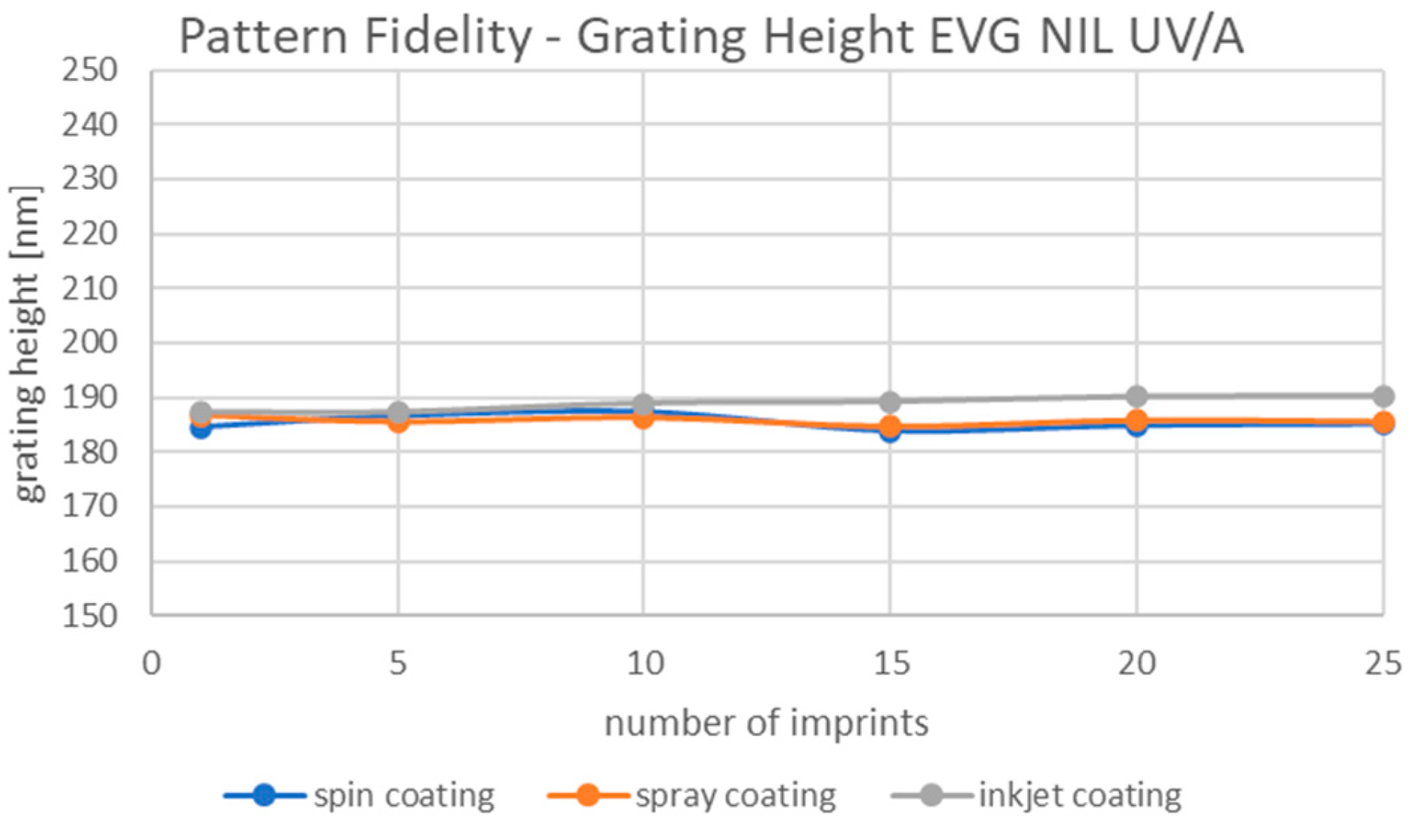
3.2. SmartNIL® Process Performance

Ensuring a reliable, stable pattern fidelity with a high number of imprints per working stamp are the main criteria to fulfill for a successful application based on SmartNIL® process. A 400 nm line/space grating template has been used to imprint 25 wafers for each type of coating process (spin, spray, and inkjet coating). The grating height was measured using AFM. Figure 10 shows a stable pattern height of 187 nm ±3 nm over 25 imprints for all three coating techniques used. These data support the conclusion that there is no influence of the coating technique when using the same working stamp with a specific geometry.
The surface roughness has been evaluated on the top surface of the imprinted gratings using AFM. The results confirm that there is no difference in the surface quality of the imprinted gratings caused by the coating method (Table 3); the AFM data show similar surface roughness with maximum Rmax < 10 nm for both materials used, the filler-free material and the one containing nanoparticles (the high refractive index material). This shows that the surface roughness of an imprint is not related to the coating technology but to the surface quality of the imprint mold.
As the high refractive index resins contain nanoparticles which limit the fluidic properties of the material, increased attention was focused on imprint results with high-resolution structures. The resolution template shown in Figure 5 was used to imprint the n = 1.9 resin, and the results were compared using AFM measurements. The AFM results show the successful replication of 100 nm pillars, wells, and lines independent from the coating technique (Table 4). These results prove that the solvent used for the dilution required for the different coating techniques and the subsequent post-coating soft bake process do not have a negative impact on the fluidic properties of the coated NIL resin and therefore on the overall imprint result.

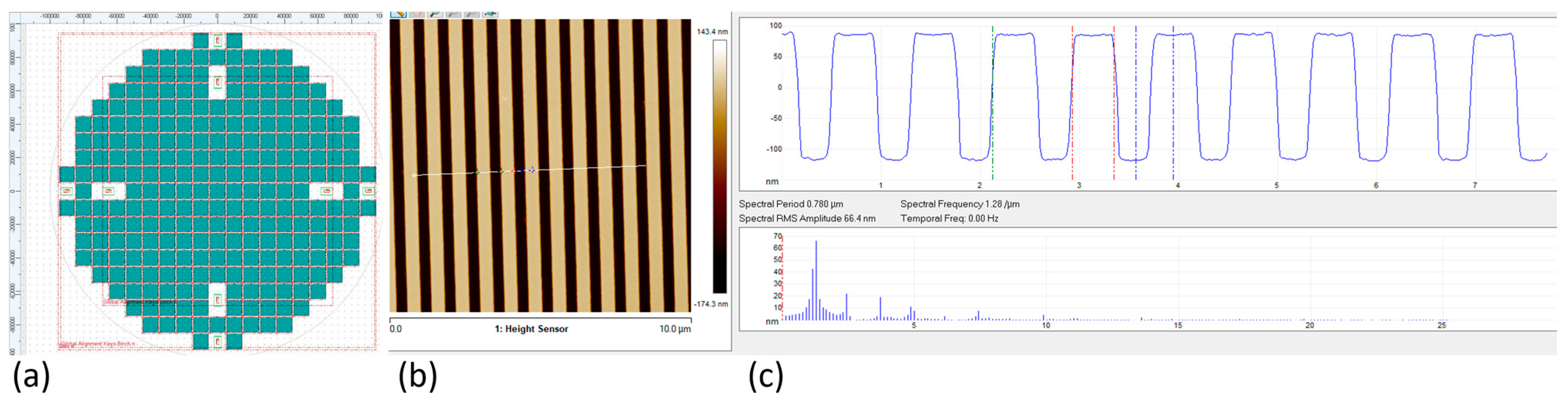
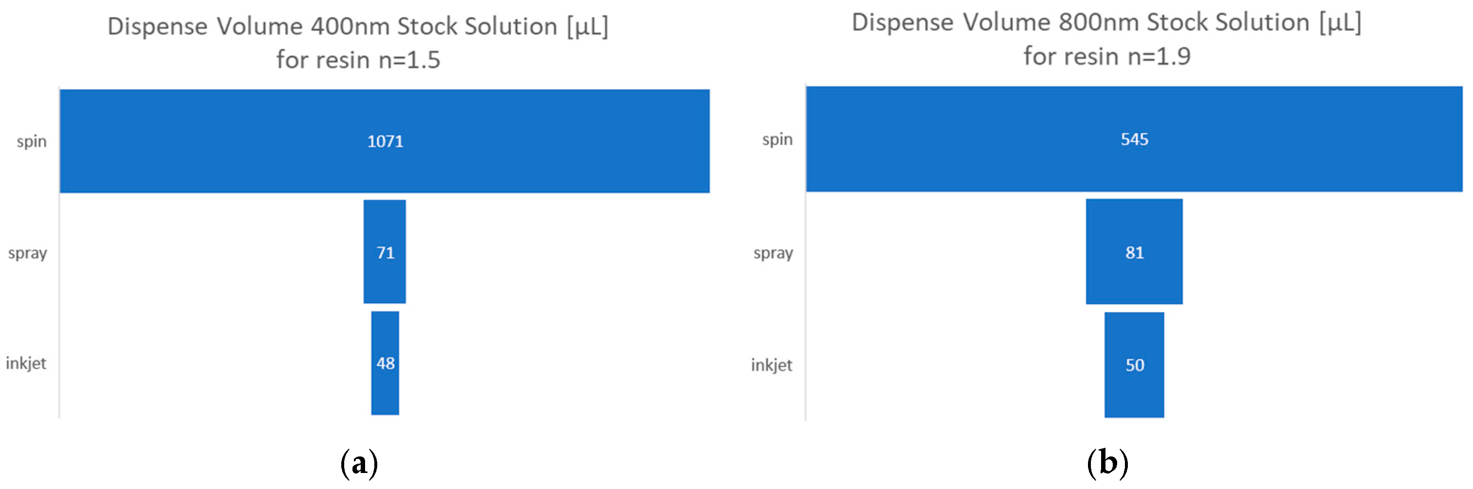
3.3. Volume Comparison

To compare the real resin consumption for achieving a 125 nm-thick layer on a 200 mm diameter wafer, standard composition solutions have been used and diluted according to the coating technology applied. For the filler-free resin, a 400 nm EVG NIL UV/A standard solution was used and modified with different solvent ratios to achieve the target layer thickness of 125 nm. As presented in Figure 11a, the filler-free resin consumption used for the spin coating process is 15 times higher compared to spray coating and 22 times higher compared to inkjet coating. This is an expected result as in the spin coating process most of the material is spun-off from the surface due to the high centrifugal forces during spinning process, whereas spray coating and inkjet coating are static coating processes. For the high refractive index resin, 800 nm standard composition solutions were used. It was necessary to dilute the standard solution for spin coating and for spray coating to achieve the target layer thickness of 125 nm, whereas the inkjet standard composition solution could be used without further modification. Figure 11b shows, similarly to the filler-free resin, a much higher resin consumption based on the standard composition solution for spin coating compared to spray and inkjet coating.
In addition to the resin consumption, the process time for coating is an important factor for production. Assuming that the process times necessary for robot handling and the final soft bake to remove the solvent are similar for all three coating techniques, inkjet coating provides the fastest coating process time (Figure 12).

4. Discussion

Spin coating is the most established coating technique in photonics and semiconductor applications, but when considering the amount of the resin volume necessary to coat a wafer compared to the amount of resin which is used to form the layer on the wafer, it is economically very inefficient, particularly when the coating resins are expensive. Additionally, a high amount of waste is created (e.g., containing nanofillers if dealing with high refractive index resins or other materials difficult to dispose of). Although the layer uniformity achieved with a spin coating process is excellent and typically within 1% variation across a 200 mm wafer, there is a disadvantage if only specific areas on the surface need to be coated. To achieve such defined resist structures, additional steps like photolithography or lift-off must be used, which require additional materials and energy consumption with a negative impact on the costs and the sustainability of a product.
Compared to spin coating, spray coating reduces the resin consumption significantly. The main disadvantage of spray coating processes for NIL resins is that this technique is—compared to spin coating—less established, and therefore, the supply chain for spray coating compatible NIL resins is not readily available, and topics like the distribution of nanoparticles in the final layer are not yet fully understood. Another negative aspect is the integration on product wafers as locally defined coating spots are difficult to realize even by using a shadow mask. Shadow masks are limited regarding spot size and require frequent cleaning procedures. A clear benefit of spray coating—in addition to the resin savings—is the possibility to coat a conformal layer on topography by choosing a solvent with a low boiling point [10,16].
Inkjet coating proved to be an interesting alternative to spin coating. While it shows similar imprint results with a layer uniformity below 5%, it entails a significant reduction in both the resin consumption and the amount of waste created. Even though the supply chain is not yet the same as that for the well-established spin coating technology, the recently emerging interest in this technology is driving resin suppliers to invest in developing inkjet resins for different applications and refractive indices. Another advantage is the possibility to adjust a layer thickness according to the layout of a device by dispensing drops on demand. This enables the formation of a uniform residual layer of an imprint even when the fill factor of the structures varies, which is crucial if the imprint is used as an etching mask. Additionally, it is possible to coat on specifically defined spots using inkjet coating which is beneficial for product integration.

5. Conclusions

In this study, spin coating, spray coating, and inkjet coating were compared as coating methods for the deposition of resins for UV-NIL. The thickness uniformity of the coated layers as well as the pattern fidelity of the final imprints were investigated for both a high refractive index material and a filler-free material. In addition, resin volume consumption and process time were compared for all three techniques.
All three techniques were found to be suitable coating methods, with spin coating and inkjet coating providing slightly better film quality and refractive index uniformity than spray coating. For the high refractive index resin containing nanoparticles, further investigation would be required to better understand the distribution of the nanoparticles in the spray-coated layer, which influences the refractive index of the final layer.
Overall, inkjet proved to be a very promising coating method for the deposition of UV-NIL resins, resulting a high layer quality similar to spin coating. Although the ability to adjust control the film thickness to suit the layout and to coat only defined areas are significant advantages over spin coating, there are still a number of challenges associated with this technology. One major issue is understanding of fluid dynamics: Due to the local deposition of single droplets, the interaction between the resin properties and the surface wetting properties is crucial for the formation of uniform resin layers [12,13,17,18,19]. Further research is therefore required to optimize and match resins, substrate surface properties, and jetting processes in order to establish inkjet coating as an alternative to spin coating for a wide number of applications.

Author Contributions

Conceptualization, C.T. and J.R.; methodology, C.T. and J.R.; investigation, C.T., J.R., P.S. and L.V.; data curation, J.R., P.S. and L.V.; writing—original draft preparation, C.T.; writing—review and editing, J.R. All authors have read and agreed to the published version of the manuscript.

Funding

The development of inkjet coating high refractive index resins was supported from the European Union’s Horizon 2020 program (Grant Agreement No. 958472).

Data Availability Statement

The original contributions presented in the study are included in the article, further inquiries can be directed to the corresponding author.

Acknowledgments

The authors would like to thank IMS CHIPS and Fraunhofer ENAS for providing the master templates which were used in this study and INKRON for supplying the high refractive index resin.

Conflicts of Interest

The authors declare no conflict of interest. All work reported here was part of the authors’ employment by EV Group, DI Erich Thallner Str. 1, 4782 St. Florian am Inn, Austria. The publication of the paper is approved and supported by the employer.

References

  1. Kast, M. High Precision Wafer Level Optics Fabrication and Integration. Photonics Spectra 2010, 44, 34–36. [Google Scholar]
  2. Thanner, C.; Dudus, A.; Treiblmayr, D.; Berger, G.; Chouiki, M.; Martens, S.; Jurisch, M.; Hartbaum, J.; Eibelhuber, M. Nanoimprint lithography for augmented reality waveguide manufacturing. In Proceedings of the SPIE AR | VR | MR, San Francisco, CA, USA, 2–4 February 2020; pp. 290–295. [Google Scholar]
  3. Dielacher, B.; Eibelhuber, M.; Uhrmann, T. High-volume processes for next-generation biotechnology devices. Solid State Technol. 2016, 59, 11–16. [Google Scholar]
  4. Schift, H. Nanoimprint lithography: 2D or not 2D? A review. Appl. Phys. A 2015, 121, 415–435. [Google Scholar] [CrossRef]
  5. Thanner, C.; Eibelhuber, M. UV Nanoimprint Lithography: Geometrical Impact on Filling Properties of Nanoscale Patterns. Nanomaterials 2021, 11, 822. [Google Scholar] [CrossRef] [PubMed]
  6. Eibelhuber, M.; Uhrmann, T.; Glinsner, T.; Lindner, P. Nanoimprint Lithography enables cost effective photonics production. Photonics Spectra 2015, 49, 34–37. [Google Scholar]
  7. ASML 2020 Annual Report. Available online: https://www.asml.com/en/investors/annual-report/2020 (accessed on 13 September 2023).
  8. Nguyen, N. Fabrication Technologies. In Micromixers, 2nd ed.; William Andrew: Norwich, NY, USA, 2012; pp. 113–161. ISBN 9781437735208. [Google Scholar]
  9. Rimböck, J.; Gasiorowski, J.; Pires, M.; Zenger, T.; Burggraf, J.; Dragoi, V. Adhesive Wafer Bonding Using Ultra-Thin Spray-Coated BCB Layers. ECS Trans. 2020, 98, 67–78. [Google Scholar] [CrossRef]
  10. Redburn, R.; Gay, K.; Monroe, M.; Oakes, G.; Sorrentino, S. Advanced MEMS and packaging: Photoresist, adhesive and thin film processing solutions for lift-off processing. In Proceedings of the IWLPC, San Jose, CA, USA, 12–14 October 2015. [Google Scholar]
  11. Levinson, H.J. Principles of Lithography, 4th ed.; SPIE Press: Bellingham, WA, USA, 2019; ISBN 978-0819456601. [Google Scholar]
  12. Derby, B. Inkjet Printing of Functional and Structural Materials: Fluid Property Requirements, Feature Stability, and Resolution. Annu. Rev. Mater. Res. 2010, 40, 395–414. [Google Scholar] [CrossRef]
  13. Martin, G.D.; Hoath, S.D.; Hutchings, I.M. Inkjet printing—The physics of manipulating liquid jets and drops. J. Phys. Conf. Ser. 2008, 105, 012001. [Google Scholar] [CrossRef]
  14. Teyssedre, H.; Landis, S.; Thanner, C.; Laure, M.; Khan, J.; Bos, S.; Eibelhuber, M.; Chouiki, M.; May, M.; Brianceau, P.; et al. A full-process chain assessment for nanoimprint technology on 200-mm industrial platform. Adv. Opt. Technol. 2017, 6, 277–292. [Google Scholar] [CrossRef]
  15. Teyssedre, H.; Landis, S.; Brianceau, P.; Mayr, M.; Thanner, C.; Laure, M.; Zorbach, W.; Eibelhuber, M.; Pain, L.; Chouiki, M.; et al. Rules-based correction strategies setup on sub-micrometer line and space patterns for 200 mm wafer scale SmartNIL process within an integration process flow. In Proceedings of the SPIE Advanced Lithography + Patterning, San Jose, CA, USA, 27 February–1 March 2017; Volume 10144, pp. 125–131. [Google Scholar]
  16. Eibelhuber, M.; Rimböck, J.; Zenger, T.; Uhrmann, T.; Matthias, T. Combined Thick Resist Processing and Topography Patterning for Advanced Metal Plating. In Proceedings of the IEEE 20th Electronics Packaging Technology Conference (EPTC), Singapore, 4–7 December 2018; pp. 191–194. [Google Scholar]
  17. Matavž, A.; Uršič, U.; Močivnik, J.; Richter, D.; Humar, M.; Čopar, S.; Malič, B.; Bobnar, V. From coffee stains to uniform deposits: Significance of the contact-line mobility. J. Colloid Interface Sci. 2022, 608, 1718–1727. [Google Scholar] [CrossRef] [PubMed]
  18. Iervolino, F.; Suriano, R.; Scolari, M.; Gelmi, I.; Castoldi, L.; Levi, M. Inkjet Printing of a Benzocyclobutene-Based Polymer as a Low-k Material for Electronic Applications. ACS Omega 2021, 6, 15892–15902. [Google Scholar] [CrossRef] [PubMed]
  19. Deegan, R.; Bakajin, O.; Dupont, T.; Huber, G.; Nagel, S.; Witten, T. Capillary flow as the cause of ring stains from dried liquid drops. Nature 1997, 389, 827–829. [Google Scholar] [CrossRef]
Figure 1. Schematic process flows of various coating techniques suitable for UV-NIL.
Nanomanufacturing 04 00005 g001
Figure 2. Schematic illustration of the general process flow.
Nanomanufacturing 04 00005 g002
Figure 3. Schematic illustration of the process flow. Steps 1–4 show the typical manufacturing steps for creating a transparent working stamp. Steps 5–8 illustrate the actual imprint process which can be repeated multiple times using the same working stamp. (Reproduced with permission from Thanner, C. and Eibelhuber, M. [5]).
Nanomanufacturing 04 00005 g003
Figure 4. Illustrations of 400 nm line/space template: (a) mask layout, (b) AFM image of structures, and (c) AFM height profile measurement of structures.
Nanomanufacturing 04 00005 g004
Figure 5. Schematic illustration of the different geometrical layouts used to investigate the filling behavior of nanostructures: (a) crossbar, (b) checkerboard, (c) meanders, (d) line and space (L/S), and (e) pillars. (Reproduced with permission from Thanner, C. and Eibelhuber, M. [5]).
Nanomanufacturing 04 00005 g005
Figure 6. Graphs showing the relation between layer thickness and different coating parameters: (a) layer thickness and dispense volume vs. spinner speed for the spin coat process; (b) layer thickness vs. dispense rate for the spray coat process; (c) layer thickness vs. droplet size (DPD).
Nanomanufacturing 04 00005 g006
Figure 7. Non-uniformity comparison of the different coating techniques for n = 1.5 and n = 1.9 resin, obtained using VASE.
Nanomanufacturing 04 00005 g007
Figure 8. Refractive index comparison over the full wavelength spectrum.
Nanomanufacturing 04 00005 g008
Figure 9. Refractive index uniformity comparison for resin n = 1.9 at 632.8 nm wavelength, obtained using VASE.
Nanomanufacturing 04 00005 g009
Figure 10. Pattern height stability over 25 imprinted wafers for resin n = 1.5.
Nanomanufacturing 04 00005 g010
Figure 11. Illustration of resin consumption referring to standard composition solutions: (a) resin n = 1.5, (b) resin n = 1.9.
Nanomanufacturing 04 00005 g011
Figure 12. Illustration of process time necessary to coat a 200 mm wafer.
Nanomanufacturing 04 00005 g012
Table 1. Overview of investigated process parameters.
Coating TechnologyConstant ParametersVariable Parameters
SpinDilution, acceleration, spin-off timeSpinner speed
SprayDilution, speed profile Dispense rate
InkjetDilution, speed profileDispense rate
Table 2. Refractive index comparison for wavelength 632.8 nm.
Refractive IndexSpin CoatingSpray CoatingInkjet Coating
n = 1.5Average 1.49Average 1.48Average 1.50
Range 1.491–1.492Range 1.475–1.476Range 1.502–1.503
n = 1.9Average 1.90Average 1.87Average 1.90
Range 1.903–1.905Range 1.856–1.883Range 1.903–1.906
Table 3. Surface roughness comparison—top surface of 400 nm imprinted gratings.
Refractive IndexSpin CoatingSpray CoatingInkjet Coating
n = 1.5Rmax: 9.4 nmRmax: 7.6 nmRmax: 9.8 nm
n = 1.9Rmax: 6.3 nmRmax: 7.2 nmRmax: 8.9 nm
Table 4. AFM images of 100 nm resolution imprints for resin n = 1.9.
100 nm Pillars100 nm Wells100 nm Lines
Spin coating n = 1.9Nanomanufacturing 04 00005 i001Nanomanufacturing 04 00005 i002Nanomanufacturing 04 00005 i003
Spray coating n = 1.9Nanomanufacturing 04 00005 i004Nanomanufacturing 04 00005 i005Nanomanufacturing 04 00005 i006
Inkjet coating n = 1.9Nanomanufacturing 04 00005 i007Nanomanufacturing 04 00005 i008Nanomanufacturing 04 00005 i009
Disclaimer/Publisher’s Note: The statements, opinions and data contained in all publications are solely those of the individual author(s) and contributor(s) and not of MDPI and/or the editor(s). MDPI and/or the editor(s) disclaim responsibility for any injury to people or property resulting from any ideas, methods, instructions or products referred to in the content.

