
Effect of Textured Glasses on Conversion Efficiency in Dye-Sensitized Solar Cells

Abstract
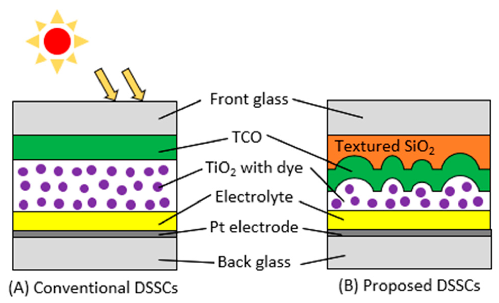
:1. Introduction
2. Methods
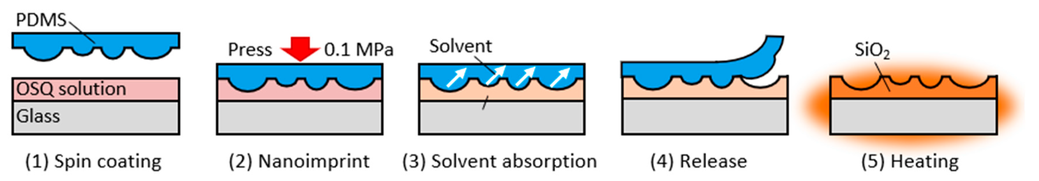
2.1. Master and Replica Molds Preparation
2.2. PDMS Nanoimprinting Process
2.3. Fabrication of DSSCs
3. Results
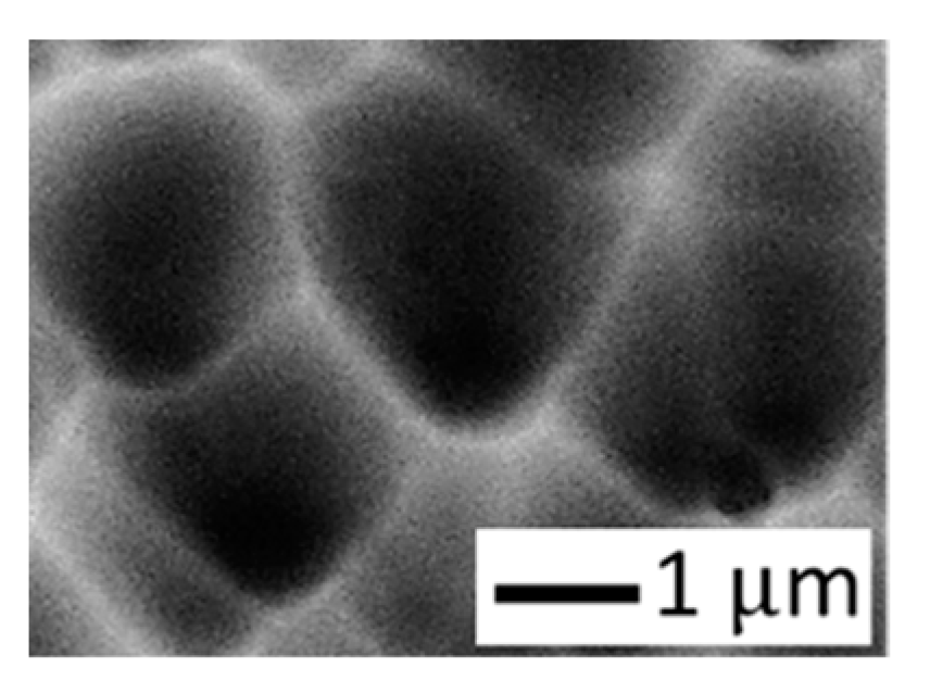
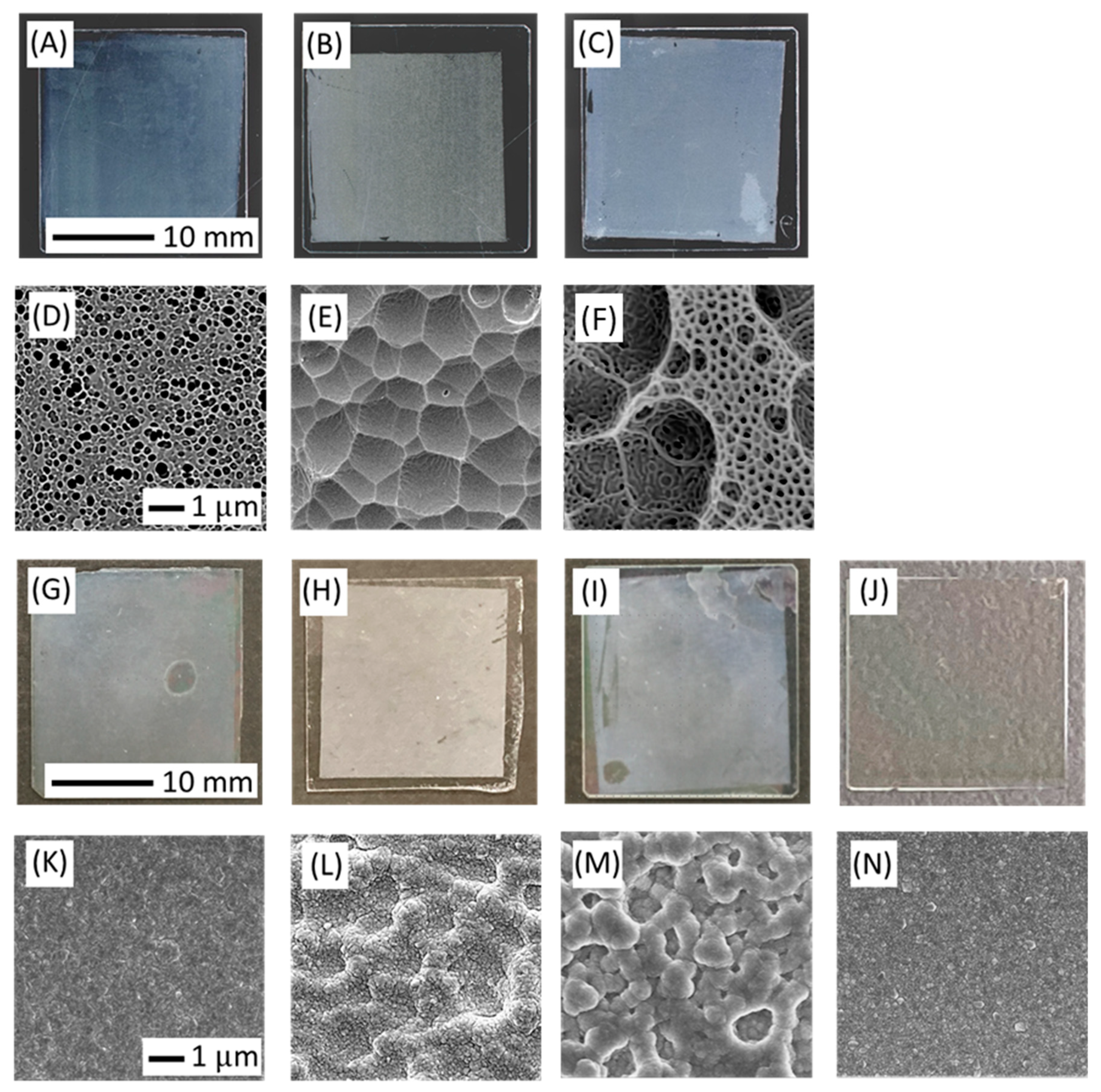
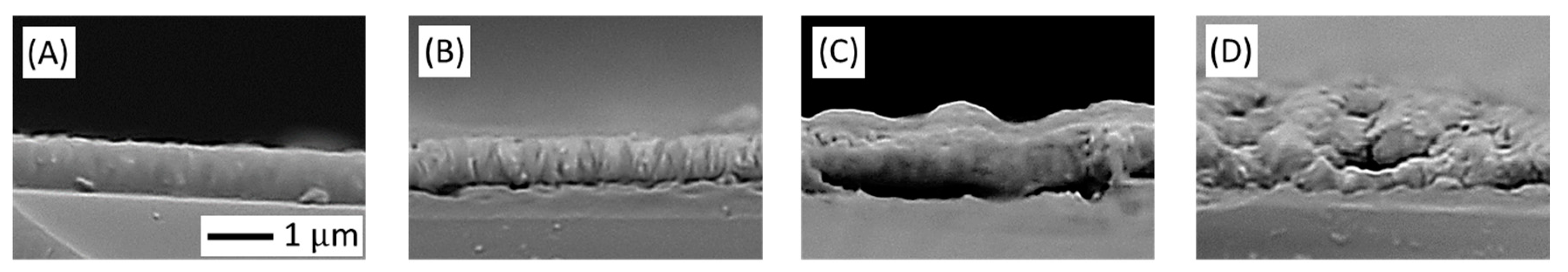
3.1. Textured Glass Substrates
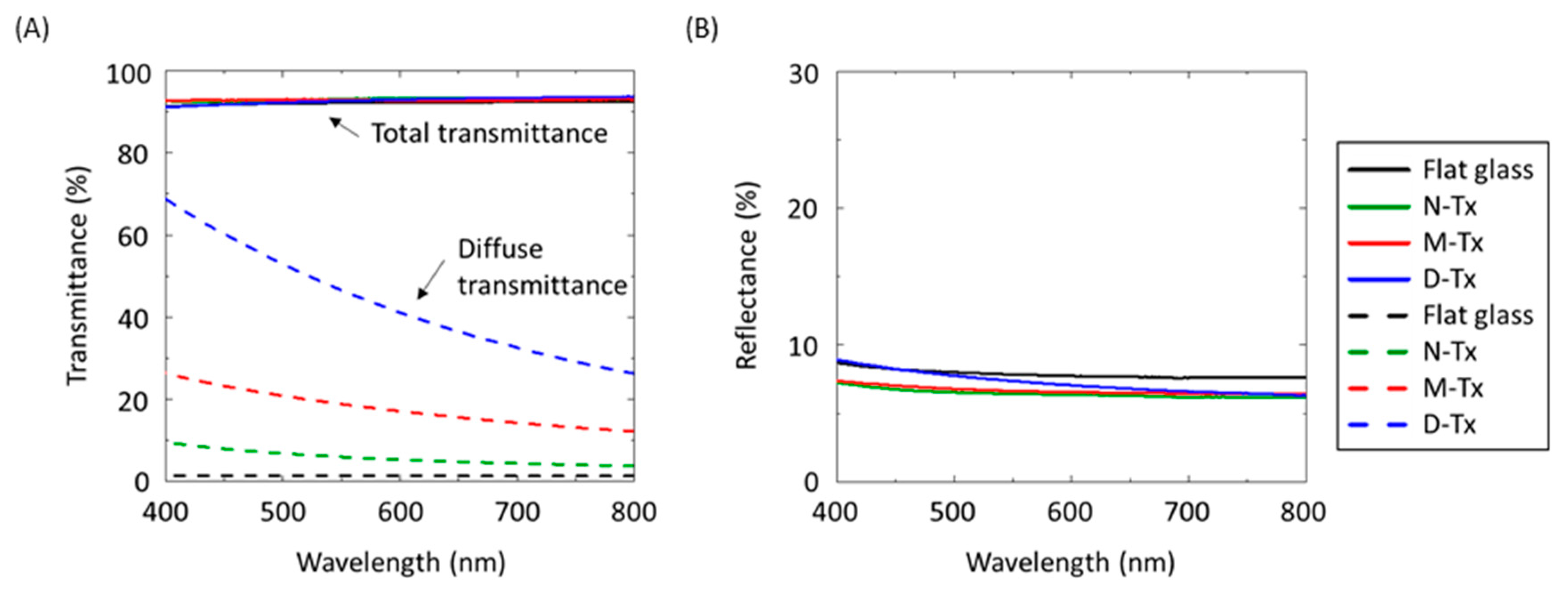
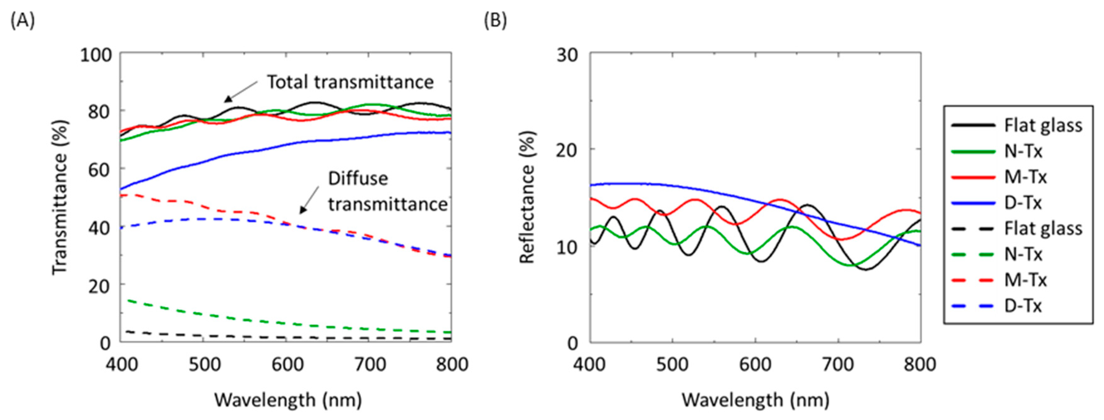
3.2. Optical Properties
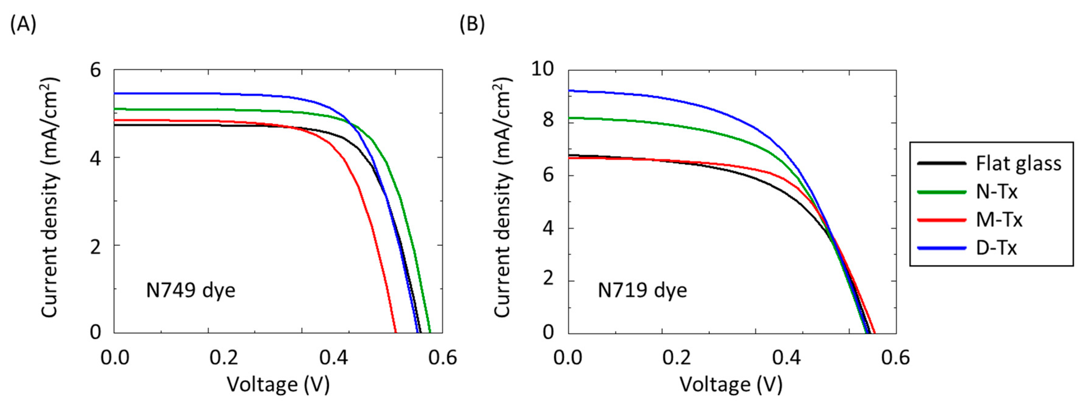
3.3. Characteristics of DSSCs
4. Discussion
5. Conclusions
Author Contributions
Funding
Data Availability Statement
Conflicts of Interest
References
- Jacak, J.; Jacak, W. Routes for Metallization of Perovskite Solar Cells. Materials 2022, 15, 2254. [Google Scholar] [CrossRef] [PubMed]
- Yang, N.; Oka, C.; Hata, S.; Sakurai, J. Fabrication of textured substrates for dye-sensitized solar cells using polydimethylsiloxane nanoimprint lithography. Adv. Opt. Technol. 2019, 8, 491. [Google Scholar] [CrossRef]
- O’regan, B.; Grätzel, M. A low-cost, high-efficiency solar cell based on dye-sensitized colloidal TiO2 films. Nature 1991, 353, 737. [Google Scholar] [CrossRef]
- Hagfeldt, A.; Boschloo, G.; Sun, L.; Kloo, L.; Pettersson, H. Dye-sensitized solar cells. Chem. Rev. 2010, 110, 6595. [Google Scholar] [CrossRef]
- Karim, N.A.; Mehmood, U.; Zahid, H.F.; Asif TKarim, N.A.; Mehmood, U.; Zahid, H.F.; Asif, T. Nanostructured photoanode and counter electrode materials for efficient Dye-Sensitized Solar Cells (DSSCs). Sol. Energy 2019, 185, 165. [Google Scholar] [CrossRef]
- Gnanasekar, S.; Kollu, P.; Jeong, S.K.; Grace, A.N.; Gnanasekar, S.; Kollu, P.; Jeong, S.K.; Grace, A.N. Pt-free, low-cost and efficient counter electrode with carbon wrapped VO2 (M) nanofiber for dye-sensitized solar cells. Sci. Rep. 2019, 9, 5177. [Google Scholar] [CrossRef] [Green Version]
- Yang, X.; Yanagida, M.; Han, L. Reliable evaluation of dye-sensitized solar cells. Energy Environ. Sci. 2013, 6, 54. [Google Scholar] [CrossRef]
- Dette, C.; Pérez-Osorio, M.A.; Kley, C.S.; Punke, P.; Patrick, C.E.; Jacobson, P.; Giustino, F.; Jung, S.J.; Kern, K. TiO2 anatase with a bandgap in the visible region. Nano Lett. 2014, 14, 6533. [Google Scholar] [CrossRef]
- Griffith, M.J.; Mozer, A.J. Porphyrin Based Dye Sensitized Solar Cells; IntechOpen: London, UK, 2011. [Google Scholar]
- Green, M.; Dunlop, E.; Hohl-Ebinger, J.; Yoshita, M.; Kopidakis, N.; Hao, X. Solar cell efficiency tables (version 57). Prog. Photovolt. 2021, 27, 3. [Google Scholar] [CrossRef] [Green Version]
- Prado, R.; Beobide, G.; Marcaide, A.; Goikoetxea, J.; Aranzabe, A. Development of multifunctional sol–gel coatings: Anti-reflection coatings with enhanced self-cleaning capacity. Sol. Energy Mater. Sol. Cells 2010, 94, 1081. [Google Scholar] [CrossRef]
- Menna, P.; Di Francia, G.; La Ferrara, V. Porous silicon in solar cells: A review and a description of its application as an AR coating. Sol. Energy Mater. Sol. Cells 1995, 37, 13. [Google Scholar] [CrossRef]
- Zhang, J.; Shen, S.; Dong, X.X.; Chen, L.S. Low-cost fabrication of large area sub-wavelength anti-reflective structures on polymer film using a soft PUA mold. Opt. Express 2014, 22, 1842. [Google Scholar] [CrossRef] [PubMed]
- Tsai, J.K.; Tu, Y.S. Fabrication of polymeric antireflection film manufactured by anodic aluminum oxide template on dye-sensitized solar cells. Materials 2017, 10, 296. [Google Scholar] [CrossRef] [PubMed] [Green Version]
- Müller, J.; Rech, B.; Springer, J.; Vanecek, M. TCO and light trapping in silicon thin film solar cells. Sol. Energy 2004, 77, 917. [Google Scholar] [CrossRef]
- Winz, K.; Fortmann, C.M.; Eickhoff, T.; Beneking, C.; Wagner, H.; Fujiwara, H.; Shimizu, I. Novel light-trapping schemes involving planar junctions and diffuse rear reflectors for thin-film silicon-based solar cells. Sol. Energy Mater. Sol. Cells 1997, 49, 195. [Google Scholar] [CrossRef]
- Mustafa, M.N.; Sumlaimah, Y. Fully flexible dye-sensitized solar cells photoanode modified with titanium dioxide-graphene quantum dot light scattering layer. Sol. Energy 2020, 212, 332. [Google Scholar] [CrossRef]
- Tsai, C.-H.; Hsu, S.-Y.; Huang, T.-W.; Tsai, Y.-T.; Chen, Y.-F.; Jhang, Y.; Hsieh, Y.; Wu, C.-C.; Chen, Y.-S.; Chen, C.-W.; et al. Influences of textures in fluorine-doped tin oxide on characteristics of dye-sensitized solar cells. Org. Electronics 2011, 12, 2003. [Google Scholar]
- Huang, S.; He, Q.; Chen, W.; Zai, J.; Qiao, Q.; Qian, X. 3D hierarchical FeSe2 microspheres: Controlled synthesis and applications in dye-sensitized solar cells. Nano Energy 2015, 15, 205. [Google Scholar] [CrossRef]
- Ahmad, Z. Increasing the efficiency of TiO2-based DSSC by means of a double layer RF-sputtered thin film blocking layer. Optik 2020, 207, 164419. [Google Scholar]
- Klimm, E.; Lorenz, T.; Weiss, K.-A. Can Anti-Soiling Coating on Solar Glass Influence the Degree of Performance Loss over Time of PV Modules Drastically? In Proceedings of the 28th EU PVSEC, Paris, France, 30 September–4 October 2013; p. 3099. [Google Scholar]
- Midtdal, K.; Jelle, B.P. Self-cleaning glazing products: A state-of-the-art review and future research pathways. Sol. Energy Mater. Sol. Cells 2013, 109, 126. [Google Scholar] [CrossRef] [Green Version]
- Wu, J.T.; Chang, W.Y.; Yang, S.Y. Fabrication of a nano/micro hybrid lens using gas-assisted hot embossing with an anodic aluminum oxide (AAO) template. J. Micromech. Microeng. 2010, 20, 075023. [Google Scholar] [CrossRef]
- Swati, S.; Mohan, P.; Kumar, V.A.; Prakash, S.S.; Sanjay, T. Enhanced photovoltaic performance via co-sensitization of Ruthenium (II)-based complex sensitizers with metal-free indoline dye in dye-sensitized solar cells. Org. Photonics Photovolt. 2017, 5, 9. [Google Scholar]


| Process | Conditions |
|---|---|
| Spin coat | 6000 rpm × 10 s |
| Press | 0.1 Mpa for Several hours |
| baking | 1st: 150 °C × 1 h |
| 2nd: 250 °C × 30 min | |
| 3rd: 480 °C × 30 min | |
| Heating rate: 20 °C/min | |
| Furnace cooling |
| Dye Texture | N749 | N719 | ||||||
|---|---|---|---|---|---|---|---|---|
| Flat Glass | N-tx | M-tx | D-tx | Flat Glass | N-tx | M-tx | D-tx | |
| η % | 2.17 | 2.41 | 1.97 | 2.38 | 2.55 | 3.01 | 2.74 | 3.22 |
| Rate of change % | - | 11 | −9 | 10 | - | 18 | 7 | 26 |
| Jsc (mA/cm2) | 4.75 | 5.11 | 4.85 | 5.48 | 6.83 | 8.19 | 6.69 | 9.22 |
| Rate of change % | - | 8 | 2 | 15 | - | 20 | −2 | 35 |
| Voc (V) | 0.65 | 0.67 | 0.60 | 0.64 | 0.65 | 0.64 | 0.66 | 0.64 |
| Rate of change % | - | 3 | −8 | −2 | - | −2 | 2 | −2 |
| FF | 0.70 | 0.70 | 0.68 | 0.67 | 0.57 | 0.58 | 0.62 | 0.54 |
| Rate of change % | - | 0 | −3 | −4 | - | 2 | 9 | −5 |
Disclaimer/Publisher’s Note: The statements, opinions and data contained in all publications are solely those of the individual author(s) and contributor(s) and not of MDPI and/or the editor(s). MDPI and/or the editor(s) disclaim responsibility for any injury to people or property resulting from any ideas, methods, instructions or products referred to in the content. |
© 2023 by the authors. Licensee MDPI, Basel, Switzerland. This article is an open access article distributed under the terms and conditions of the Creative Commons Attribution (CC BY) license (https://creativecommons.org/licenses/by/4.0/).
Share and Cite
Kimura, R.; Nishiyasu, Y.; Oka, C.; Hata, S.; Sakurai, J. Effect of Textured Glasses on Conversion Efficiency in Dye-Sensitized Solar Cells. Nanomanufacturing 2023, 3, 315-325. https://doi.org/10.3390/nanomanufacturing3030020
Kimura R, Nishiyasu Y, Oka C, Hata S, Sakurai J. Effect of Textured Glasses on Conversion Efficiency in Dye-Sensitized Solar Cells. Nanomanufacturing. 2023; 3(3):315-325. https://doi.org/10.3390/nanomanufacturing3030020
Chicago/Turabian StyleKimura, Ryutaro, Yuji Nishiyasu, Chiemi Oka, Seiichi Hata, and Junpei Sakurai. 2023. "Effect of Textured Glasses on Conversion Efficiency in Dye-Sensitized Solar Cells" Nanomanufacturing 3, no. 3: 315-325. https://doi.org/10.3390/nanomanufacturing3030020