1. Introduction
In addition to the opaque solar cells used for conventional installations in photovoltaic plants or buildings roofs, new semitransparent photovoltaic systems are being developed for applications in skylights and windows [
1,
2]. Semitransparent cells are designed to convert a portion of the solar irradiance into electricity while transmitting the remaining sunlight into the building. They can also reduce the cooling load in summer by reducing radiation indoors while maintaining visible comfort [
3].
Among the various semiconductor materials that can act as photovoltaic absorbers, compounds with a chalcopyrite structure such as CuInSe
2, CuGaSe
2 and CuIn
1-xGa
xSe
2 have demonstrated long-term stability and high conversion efficiencies at low manufacturing costs [
4,
5]. The analogous sulfide chalcopyrites, CuInS
2 and CuGaS
2, are now of renewed interest due to their broader bandgap, which make them good candidates for semitransparent devices [
6,
7,
8]. Also, the newly discovered wurtzite (cation-disordered) polytype of CuInS
2 [
9], as well as the wurtzite ZnSnN
2 [
10] and mixed ZnSnN
2 (cation-ordered and -disordered phases) [
11], all have similar absorption coefficient values. The chalcopyrite absorbers are commonly prepared as thin films on glass substrates [
4,
7], because their high absorption coefficient (~10
4 cm
−1) allows a low thickness (~1 μm) to be used to absorb the radiation energy greater than the bandgap [
12]. Therefore, semitransparency can be straightforwardly achieved by growing thinner chalcopyrite layers below the absorption length in the visible spectral range [
13], resulting in less material consumption and reduced deposition time as additional advantages [
12,
13]. Considering that the maximum photovoltaic conversion efficiency is 23% for chalcopyrite semiconductors with 2.0 μm thickness [
12], high efficiencies of around 8% have also been reported for a thickness of 200 nm [
12] and 3% for a thickness of 50 nm [
13].
Solar radiation undergoes various absorptions in the Earth’s atmosphere, and the average energy falling on the Earth’s surface at air-mass 1.5 (AM1.5) is the standard spectrum applied to test the conversion efficiency of photovoltaic cells [
4,
12], which is used here to determine the solar absorptance (α
S). On the other hand, for transparent and semitransparent building elements, European directives define luminous transmittance (τ
L) [
14] and colorimetric calculations [
15] based on the standard illuminant D65, which represents the typical spectral distribution of daylight in clear conditions at around noon [
16]. It should be noted that luminous transmittance takes into account the eye’s sensitivity to different wavelengths through standard photopic vision (V) [
14], and a value of τ
L~10% is considered sufficient to obtain a comfortable soft daylight effect [
2,
17]. The product of the conversion efficiency and the luminous transmittance is a single compound parameter called light utilization efficiency (LUE) [
18], which allows the comparison of different semitransparent solar cells.
The color perception is another parameter to consider, because in most cases the optical transmittance in the visible wavelength region is not uniform. The correlated color temperature (CCT) and average color rendering index (R
a) are the two main criteria for evaluating whether the natural light transmitted through glazing provides aesthetic comfort [
19]. CCT is the temperature of a black-body radiator that has the closest chromaticity to the illuminant (a light source alone or through a transparent medium), allowing the interior light to be distinguished in neutral (3000 K ≤ CCT ≤ 5000 K), bluish white (CCT > 5000 K) or yellowish white (CCT < 3000 K) [
20]. Furthermore, R
a describes quantitatively how accurately the test light reproduces the color of a given object with respect to a perfect reference illuminant [
15]. Although, in a strict sense, R
a can only be compared for two illuminants that have the same CCT, in practice, R
a values are also given with respect to a single reference (usually the standard D65), because this provides direct information about the indoor illumination through semitransparent glasses that correspond to different CCTs [
19,
20]. In any case, an index of 60% ≤ R
a ≤ 79% is considered good color rendering and R
a ≥ 80% is considered excellent [
18,
21].
In the present work, the optical absorption coefficients of various chalcopyrite thin films (CuInSe2, CuInS2 and CuGaS2 grown by evaporation) were analyzed to test their suitability to be applied in semitransparent photovoltaic glazing. The solar absorptance, luminous transmittance and color rendering index were determined and then combined into a single parameter (a new figure of merit) that was calculated for each chalcopyrite compound based on the respective thickness. This allows for a better evaluation of visual comfort and explores the possibility of reducing material consumption by comparing the optimal absorber thickness for each compound. The correlated color temperature of the transmitted light is linked to the color rendering index and is therefore implicitly included in the figure of merit.
2. Materials and Methods
Chalcopyrite CuInSe
2, CuInS
2 and CuGaS
2 thin films were prepared by means of modulated flux deposition in a custom-designed vacuum chamber [
22]. Within the chamber, a rotating holder span soda-lime glass substrates at 30 rpm for evaporation induced by Cu, In, and Ga beam sources, heating to 350 °C by halogen lamps, and a reaction with vapor from elemental Se or S sources in every rotation. All of the base materials were pellets with 99.99% purity. The metals (Cu, In, Ga) were evaporated from shuttered molecular beam effusion cells, which consisted of a water-refrigerated Mo case with a PBN crucible liner surrounded by a heating filament. The chalcogens (Se, S) were evaporated from two-stage Pyrex glass cells with an intermediate valve that separated the evaporating and cracking stages, which could be set at different temperatures. Flux control of all sources was achieved using Eurotherm 902 temperature controllers.
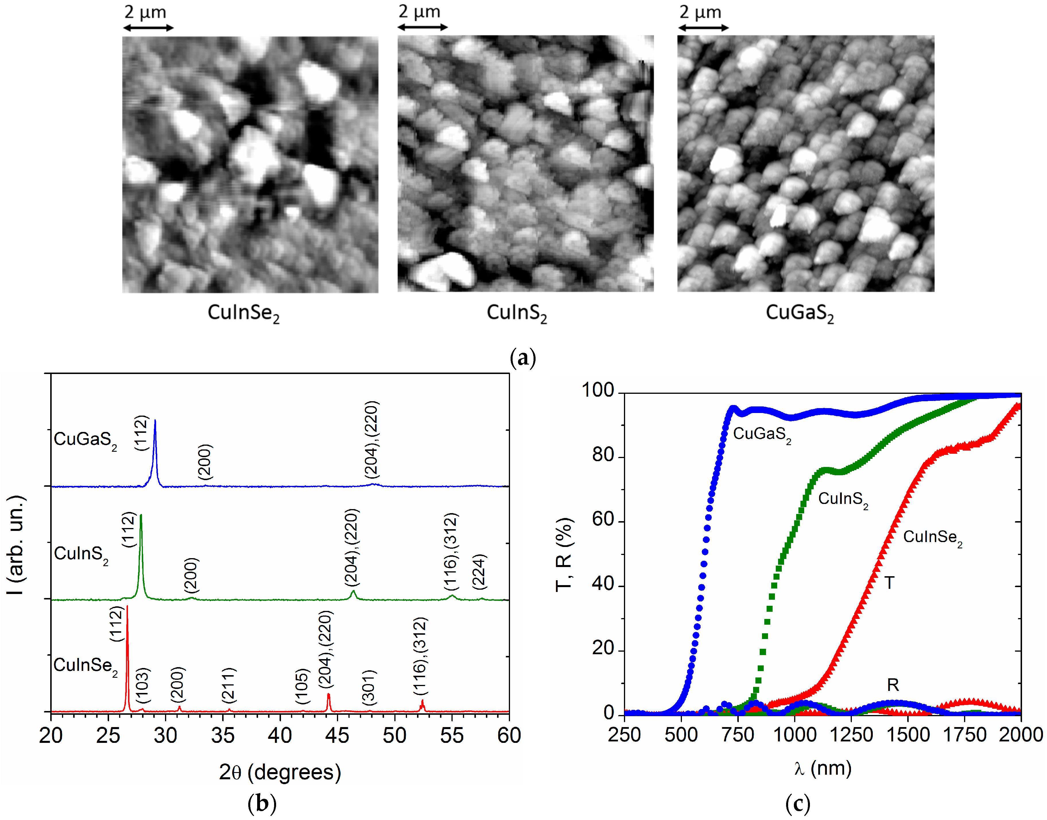
The structural, morphological and optical properties of these films were analyzed in a previous work [
23], where the surface morphology was examined via atomic force microscopy (AFM) with a Park XE-100, and the tetragonal chalcopyrite structure was identified by means of X-ray diffraction (XRD) performed in a Philips X’pert instrument with radiation CuKα (λ = 1.54056 Å) and a Bragg–Brentano θ–2θ configuration.
Figure 1a shows representative AFM images and
Figure 1b displays the diffraction patterns corresponding to 600 nm thick films, where all the peaks are indexed according to the standard powder diffraction files for chalcopyrite CuInSe
2 (card file no. 40-1487), CuInS
2 (no. 27-0159), or CuGaS
2 (no. 25-0279), without secondary phases.
The transmittance (T) and reflectance (R) of these chalcopyrite layers are represented in
Figure 1c, which were measured with a double beam spectrophotometer Perkin-Elmer Lambda 9, taking the glass substrate as a reference (T
glass = 100% and R
glass = 0%). Then, the optical absorption coefficient was calculated as follows [
24]:
including film thickness (t = 600 nm for the samples in
Figure 1).
The optical absorption coefficients were obtained for specific thickness and transmittance values and then extrapolated to obtain the spectra of transmittance and absorptance [
12] for different film thicknesses:
This calculated spectra are used in
Section 3 to evaluate the solar absorptance, as well as the luminous transmittance and color rendering properties of chalcopyrite CuInSe
2, CuInS
2 and CuGaS
2 depending on their respective thickness.
2.1. Determination of the Solar Absorptance and Luminous Transmittance
For each compound and thickness value, the solar radiation that can be collected is given by the product of the standard AM1.5 irradiance (S) and the chalcopyrite absorptance (A) at each wavelength [
18]. The photovoltaic performance is thus related to the solar absorptance (α
S), defined as the percentage of the total solar irradiance that is absorbed in the film:
On the other hand, the luminous transmittance (τ
L) denotes the fraction of the incident light coming from the D65 illuminant that is transmitted by the glazing and is viewed by a standard photopic observer V [
14]:
where T(λ) is the chalcopyrite transmittance.
2.2. Determination of the Correlated Color Temperature
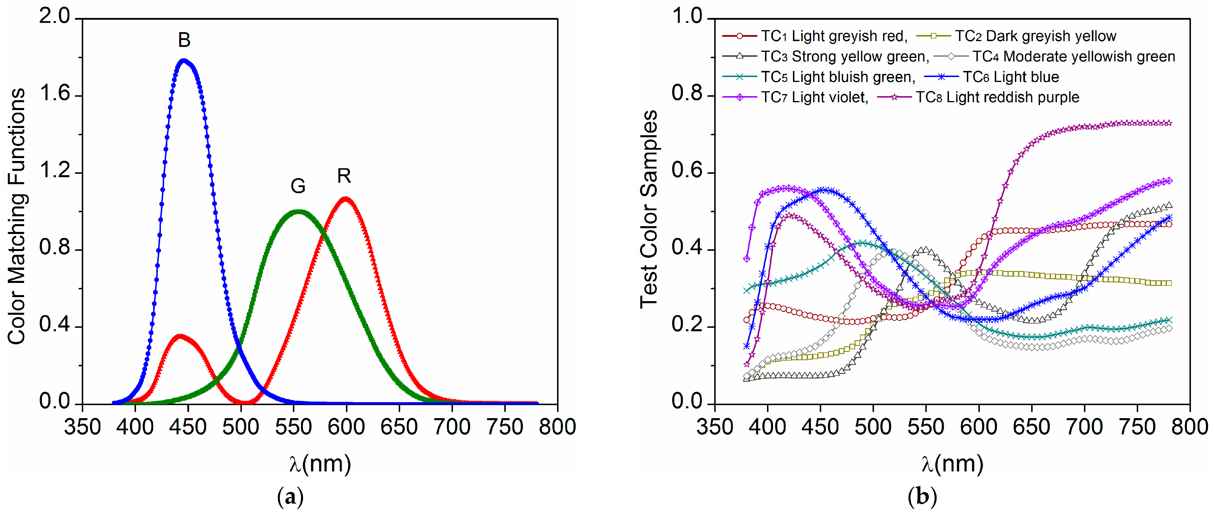
According to the International Commission of Illumination (CIE) [
15], the tristimulus values XYZ (in the 1931 CIE color system) indicate how much red, blue and green an illumination source contains. In this work, these contents were calculated for the transmitted light from the standard D65 illuminant, with the color matching functions (R, G and B) shown in
Figure 2a, as follows:
Next, the dimensionless chromaticity coordinates
x and
y (1931 CIE) for the transmitted light were calculated:
and the correlated color temperature given by [
19]:
Likewise, the reference values are:
This resulted in Xr = 95.047, Yr = 100, Zr = 108.883, which give xr = 0.3127, yr = 0.3290 and CCT = 6504 K for the standard D65 reference.
2.3. Determination of the Color Rendering Index
For color rendering evaluation according to CIE directives [
15], we needed to calculate the tristimulus values of the light transmitted by the chalcopyrite film for each of the eight test colors (TC
i, with i = 1 to 8), as shown in
Figure 2b:
Next, the uniform color space coordinates u and v (1960 CIE) for the transmitted light were calculated:
Likewise, u
r,i and v
t,i were calculated from the reference coordinates:
Furthermore, Equation (6a–c) produce (ut, vt) values that depend on the chalcopyrite transmittance and Equation (10a–c) provide ur = 0.1978 and vr = 0.2967 for the standard D65 illuminant.
The adaptive color shift was then applied to compensate for the color appearance deviation of each test color sample illuminated under test and reference illuminants, defined as follows:
and the coordinates:
For the standard D65: cr = 2.8150, dr = 2.0823, .
After considering the adaptive color shift, the colorimetric data were transformed according to the 1964 CIE system as follows:
The difference in rendering of a test color sample illuminated directly by the reference illuminant and by the same illuminant transmitted through the chalcopyrite film was quantified as follows:
Finally, the average color rendering index for the eight test colors was
3. Results and Discussion
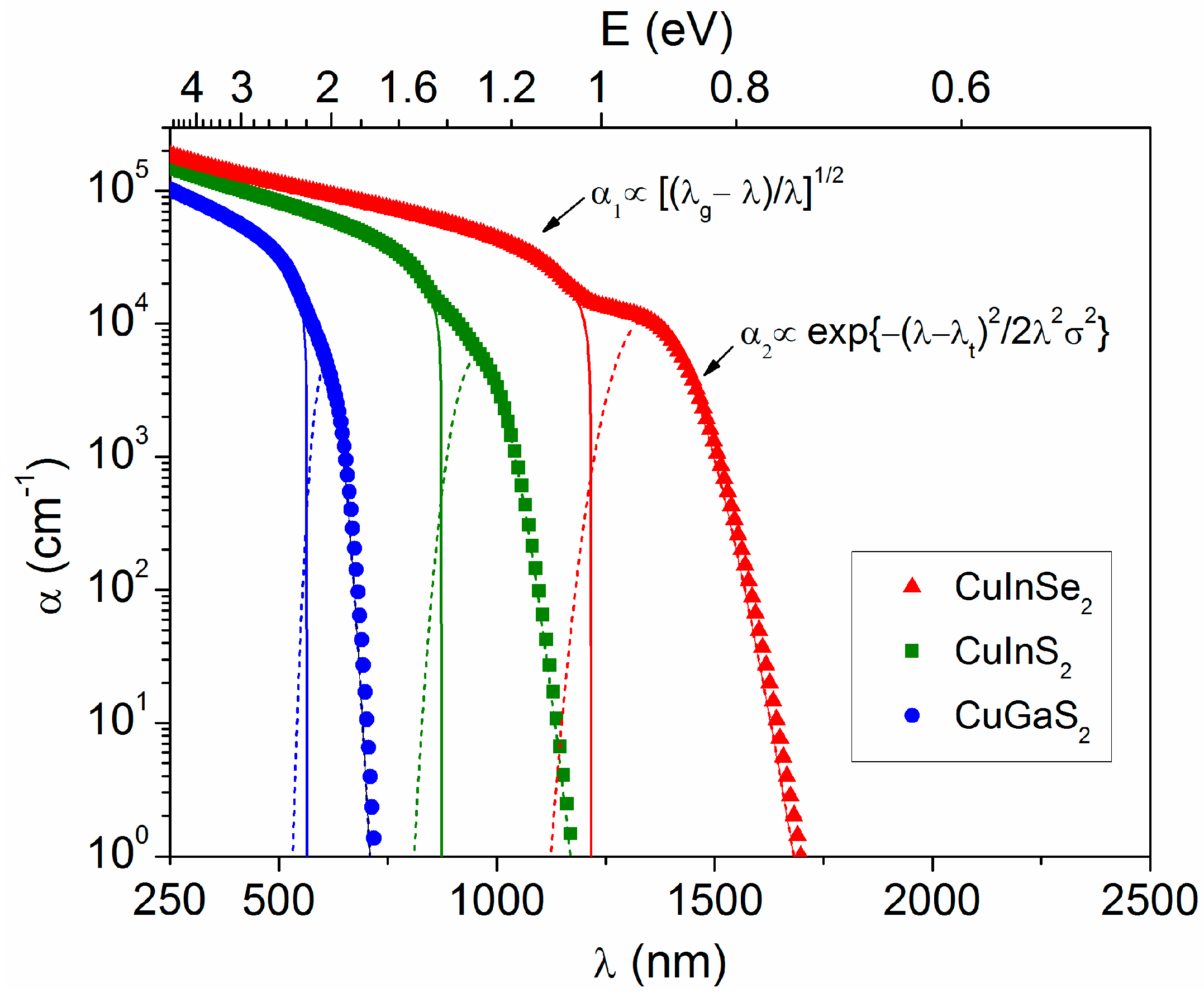
All the evaporated chalcopyrite films have high absorption coefficients within the visible spectral range, especially at wavelengths λ < 600 nm or energies E > 2.07 eV, as represented in
Figure 3. Compared to CuGaS
2, the absorption extends towards the near infrared region for CuInS
2 and further for CuInSe
2 due to the difference in bandgap energy (E
g) for each material [
25]. Although the representation of α vs. E is the most used,
Figure 3 shows the dependence of α vs. λ (being E = hc/λ) to better illustrate the subsequent calculations that are made in terms of wavelengths. In the high absorption region (α > 10
4 cm
−1), the experimental data show a good fit to the expression that corresponds to direct transitions for polycrystalline semiconductors [
26]:
giving the gap wavelength λ
g = 560 nm for CuGaS
2, λ
g = 870 nm for CuInS
2 and λ
g = 1220 nm for CuInSe
2, in good agreement with the literature, which establishes direct transitions for chalcopyrite compounds [
25,
27,
28]. The presence of some absorption at λ > λ
g (or E < E
g) is due to tail states that are also typical of chalcopyrite materials [
29]. In this other region, the absorption coefficient can be fitted to the form
where λ
t is a characteristic transition wavelength and σ represents the width of the tail [
30,
31]. When plotted in wavelengths, the tail width appears larger for CuInSe
2 than for CuInS
2 and CuGaS
2, but when expressed in energy, the width is similar for all three compounds, σ~60 meV, in the same order reported for analogous photovoltaic absorbers [
32]. The tail wavelength is found at λ
t = 610 nm for CuGaS
2, λ
t = 960 nm for CuInS
2 and λ
t = 1350 nm for CuInSe
2, slightly above the respective gap wavelength.
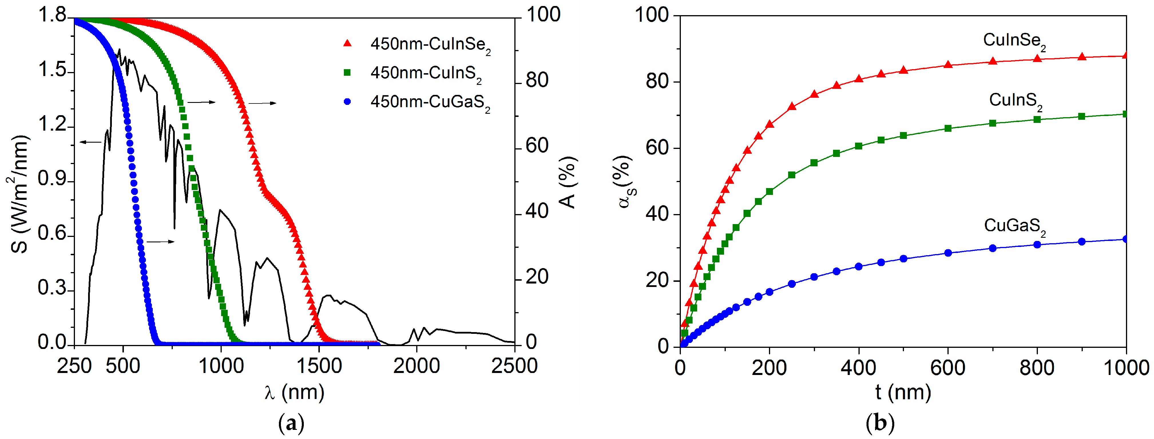
The incident solar irradiance is illustrated in
Figure 4a for the standard AM1.5, which has an integrated value
993 W/m
2, being 4% in the ultraviolet region (λ = 250–380 nm), 53% in the visible region (λ = 380–780 nm), and 43% in the near infrared region (λ = 780–2500 nm) [
33].
Figure 4a also includes the absorptance spectra corresponding to 450 nm thick chalcopyrite films in order to compare the optical characteristics of the different compounds with the solar irradiance. Moving on to a quantitative evaluation,
Figure 4b represents the percentage of total solar irradiance that is absorbed by each chalcopyrite compound, calculated from Equation (4) depending on the film thickness. The solar absorptance increases quickly with the thickness up to t~450 nm, at which point a value of α
S = 26% is obtained for CuGaS
2, α
S = 62% for CuInS
2 and α
S = 82% for CuInSe
2. However, the increment for each compound is only about 6% from t = 450 nm to t = 900 nm. On the other hand, a value of α
S = 26% is obtained for 80 nm thick CuInS
2 and 45 nm thick CuInSe
2. The comparative analysis indicates that 70 nm thick CuInSe
2 absorbs as much solar irradiance (α
S = 37%) as 130 nm thick CuInS
2 and 900 nm thick CuGaSe
2.
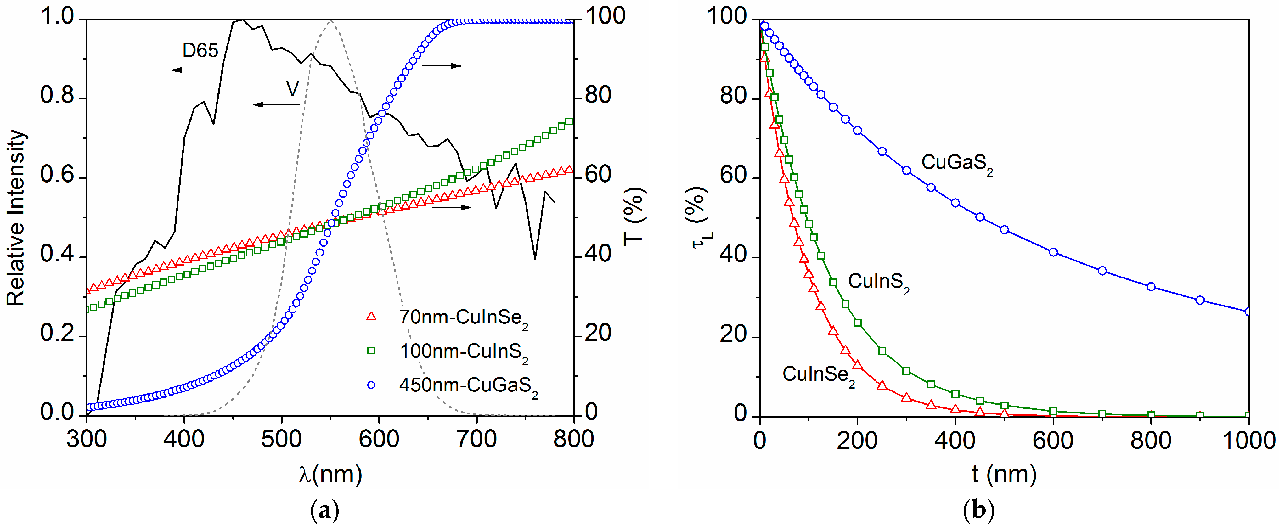
The spectral distribution of the standard illuminant D65 and standard photopic vision V are represented in
Figure 5a, along with the transmittance spectra corresponding to several chalcopyrite thin films for comparison. All of these spectra are used to calculate the luminous transmittance according to Equation (5) for the different chalcopyrite compounds, which is plotted in
Figure 5b as a function of the respective film thickness. While reference D65 covers the entire visible region, photopic vision is restricted to the small range where the human eye has sensitivity [
34], with a maximum centered at λ
V = 550 nm. Therefore, τ
L is actually given by the transmittance values in a very narrow region around λ
V, although the average transmittance over the whole visible range may be different. For CuInSe
2 and CuInS
2, the luminous transmittance decreases quickly with the film thickness, being τ
L < 10% for t ≥ 300 nm and τ
L < 1% for t ≥ 600 nm, with τ
L= 40% for 90 nm thick CuInSe
2 and 130 nm thick CuInS
2. Meanwhile, for CuGaS
2, the luminous transmittance remains high, even with thicker layers (τ
L = 29% for t = 900 nm). The same value of τ
L = 50% is obtained for 450 nm thick CuGaS
2, 100 nm thick CuInS
2 and 70 nm thick CuInSe
2, but they have different transmittance distributions (shown in
Figure 5a), which is taken into account by the color rendering index.
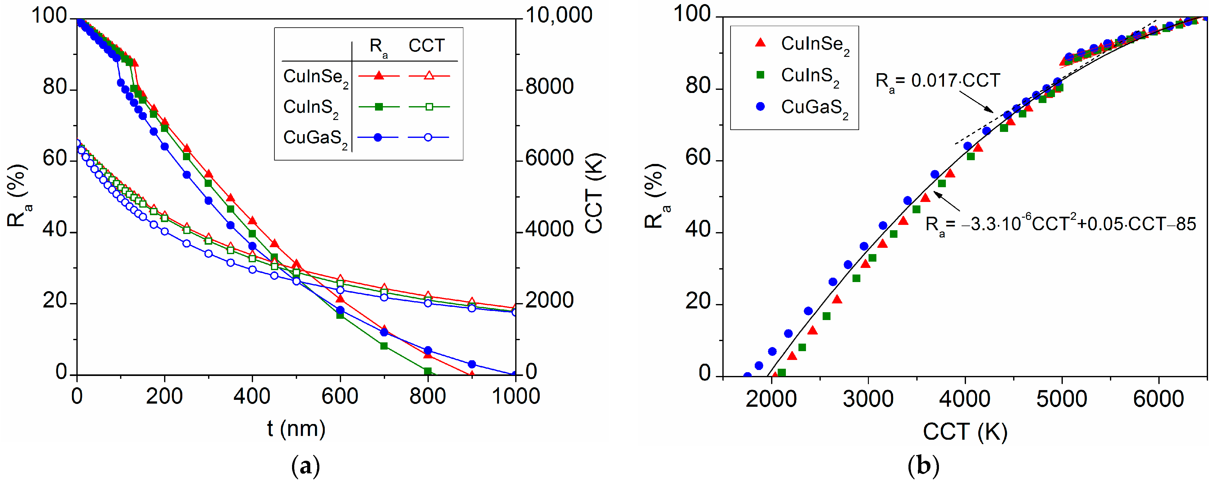
Figure 6a depicts the evolution of the average color rendering index, R
a, calculated using Equation (19), and the correlated color temperature, CCT, calculated using Equation (9), depending on the chalcopyrite film thickness. An analogous behavior is observed for these parameters, both decreasing as the film thickness increases, and similar values are observed for the three chalcopyrite compounds, despite their different luminous transmittances. In fact, for a given thickness, R
a and CCT are found to be slightly higher for CuInSe
2 and CuInS
2 than for CuGaS
2, contrary to their respective τ
L values shown in
Figure 5b. This is because not only a higher transmittance but also smoother variations in the visible range provide better color rendering [
35]. According to the criteria for semitransparent glazing [
19], a good index R
a ≥ 60% is obtained for the various chalcopyrite compounds with thickness t ≤ 250 nm, and an excellent R
a ≥ 80% is obtained for t ≤ 130 nm. Regarding the color temperature of the transmitted light, the values CCT > 3000 K for t ≤ 400 nm are considered suitable for visual comfort [
36]. The correlation of CCT and R
a is illustrated in
Figure 6b, where the data obtained for the different chalcopyrite films follow a parabolic relationship:
. Some authors report a linear fit
for dye sensitized solar cells, although only in the range of 3500 K < CCT < 5500 K.
Figure 6b shows that the linear relationship also applies to the chalcopyrite data in a short CCT region, but R
a decreases quickly for CCT < 3500 K, as observed for other semitransparent devices [
37].
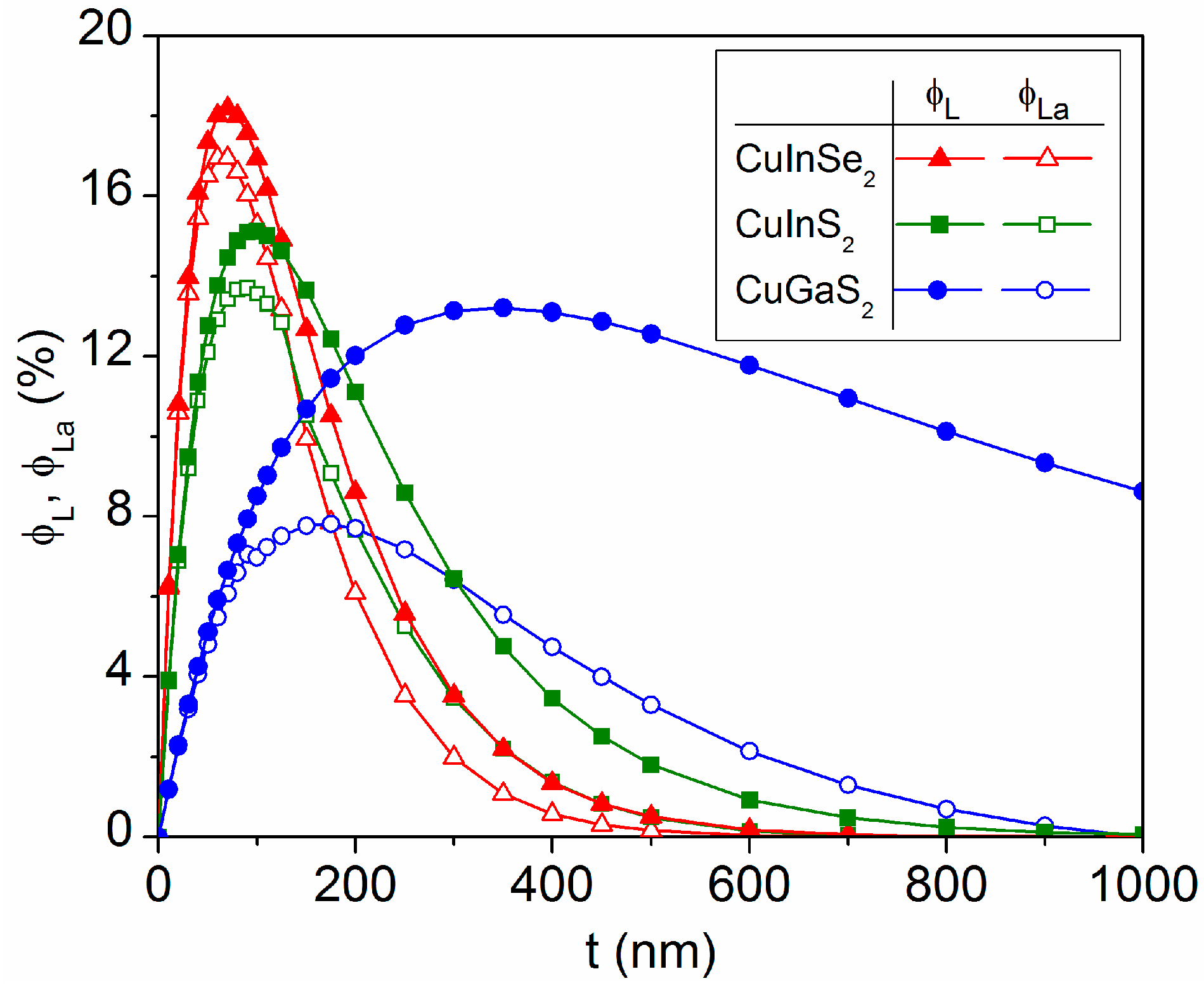
In order to better evaluate these chalcopyrite materials for application in semitransparent solar cells, a figure of merit can be defined as the product of the solar absorptance and luminous transmittance:
which is analogous to the light utilization efficiency used for photovoltaic devices [
18,
35], but replacing the conversion efficiency with α
S to consider only the absorber material. Furthermore, to take into account the color rendering, it is interesting to define another figure of merit in the form:
which includes the two optical parameters (τ
L and R
a) that describe the visual comfort.
Figure 7 presents both
and
for the various chalcopyrite compounds as a function of the film thickness. The best results are obtained for CuInSe
2 (with maximum
= 18% and
= 17% for t = 70 ± 20 nm), followed by CuInS
2 (maximum
= 15% and
= 14% for t = 90 ± 30 nm) and CuGaS
2 (with maximum
= 13% for t = 350 ± 100 nm and maximum
= 8% for t = 180 ± 50 nm). The difference between
and
is larger for CuGaS
2 due to its relatively lower R
a index. In addition, it should be noted that all three compounds give the same value
= 8% for t~180 nm, but CuInSe
2 and CuInS
2 can achieve higher
with a lower thickness, requiring less material consumption and reduced deposition time as additional advantages. For semitransparent solar cells, an absorber layer as thin as 30 nm has been reported [
13].
4. Conclusions
The evaporated chalcopyrite thin films have shown high optical absorption coefficients below the respective gap wavelength (α > 104 cm−1 at λ < λg), which increases from λg = 560 nm for CuGaS2 to λg = 870 nm for CuInS2 and λg = 1220 nm for CuInSe2, with some additional absorption slightly above λg due to band tails. The experimental coefficients obtained for each chalcopyrite compound provide absorptance and transmittance spectra that depend on the film thickness and allow a comparative analysis of the solar absorptance, luminous transmittance and color rendering index. Regarding the correlated color temperature of the transmitted light, also considered as a factor for visual comfort, it is directly related to the color rendering index through a parabolic relationship.
According to the criteria for semitransparent glazing, a good index Ra ≥ 60% (CCT ≥ 4000 K) is obtained for the three chalcopyrite compounds with thickness t ≤ 250 nm, and an excellent Ra ≥ 80% (CCT ≥ 4800 K) is obtained for t ≤ 130 nm. For a given thickness, Ra is slightly higher for CuInSe2 and CuInS2 than for CuGaS2, contrary to their respective τL values, due to the smoother variation of CuInSe2 and CuInS2 transmittances in the visible region. Otherwise, the absorbed solar irradiance increases with the film thickness faster for CuInSe2 and CuInS2 than for CuGaS2.
The product of the solar absorptance, luminous transmittance and color rendering index is considered here as a new figure of merit, , to evaluate these absorber materials for their incorporation into semitransparent solar cells. Applying this quantification, the best result corresponds to CuInSe2 (with maximum = 17% for t = 70 ± 20 nm), followed by CuInS2 (maximum = 14% for t = 90 ± 30 nm) and CuGaS2 (maximum = 8% for t = 180 ± 50 nm). These data provide guidelines for the design of semitransparent photovoltaic devices based on chalcopyrite absorbers.


