1. Introduction
Layered 2D semiconductors have recently become widely studied materials as they can be applied in nanosized transistors, photodetector LEDs, solar cells and sensing devices [
1]. Due to their atomically smooth surfaces, the built-in trap concentration can be minimal, and therefore more stable and higher performance devices can be fabricated from them [
2]. 2D materials with sizable bandgaps, such as transition metal dichalcogenides (TMD), have been the focus of research, as they do not possess the drawback of the absence of an intrinsic band gap in graphene [
3]. TMDs can be denoted as MX
2, where M is the transition metal and X is the chalcogen. As transition metals have varying numbers of d-electrons, TMDs also have different electronic properties, different sized band gaps and room temperature mobilities, giving way to new technological possibilities [
4].
HfS
2 is a less examined member of the TMD family, with most properties only theoretically predicted and few reliable ways to synthesize. According to calculations, HfS
2 may have ultrahigh room-temperature electron mobility and sheet current density, combined with high chemical stability and reasonable bandgap. Therefore, it could be a very promising material for the transistors, photocatalysts and photodetectors of the future [
5,
6]. HfS
2 has 1T (tetragonal symmetry, one layer per unit with octahedral coordination) crystal structure.
There are only a handful of publications describing the preparation or properties of HfS
2 compared to other TMDs. Most are theoretical calculations predicting the promising high mobility and current density of the material. On the other hand, the different models predict different band gaps depending on the pseudopotentials used and ground-state structures. Density functional theory calculations suggest a 1.13 eV wide indirect bandgap [
7]. In contrast, hybrid functional methods show that the indirect bandgap of HfS
2 increases with the decreasing layer thickness, from 2.7 eV at 5 monolayers to 2.98 eV at a monolayer thickness [
3,
8]. Experimental results suggest that the bandgap of bulk HfS
2 is around 2 eV [
9,
10].
The preparation of HfS
2 films has also met some difficulties. Most experimental procedures are based on mechanical exfoliation, but with this method, only small flakes can be synthesized [
11,
12,
13]. The chemical vapor deposition of HfS
2 has also proved possible typically by utilizing the chemical reaction of HfCl
4 and elemental S powder [
14,
15]. Still, these have also only been possible on laterally small substrates and at high temperatures (900–1000 °C). A reliable preparation of HfS
2 layers on wafer-sized surfaces would be extremely important for later applications, but it has not been solved yet.
Atomic layer deposition (ALD) is a vapor phase layer deposition method based on self-limiting surface reactions on heated substrate surfaces due to the chemisorption of separate pulses of precursors. ALD is used for the preparation of elements, oxides, nitride, sulfides, and complicated compounds as well [
16,
17,
18]. As the thickness of the deposited layers can be controlled on the atomic level, ALD appears to be a perfect method for the development of 2D materials. Due to the large-scale uniformity and conformity of the ALD deposited layers, the method offers the possibility of the development of wafer-scale 2D materials, which has been lacking so far. There are three main approaches to the preparation of 2D films: The most widespread is the controlled layer-by-layer growth of the required material to the required thickness [
1]. The second is the self-limiting layer synthesis process, in which the number of layers is determined by the temperature [
19]. Finally, it is also possible to deposit a precursor film with ALD and then achieve the required stoichiometry post-treatment [
20].
The ALD of HfS
2 has not yet been explored. There are, so far, only three papers describing the ALD of HfS
2 films. Mattinen et al. [
21] tried the reactions of HfC
4, HfI
4 and Hf(NEtMe)
4 with H
2S. The latter two of these precursor materials yielded non-uniform and rough layers. Thus, the HfCl
4-H
2S process seemed the most promising, resulting in amorphous HfS
2 films in the deposition temperature range of 200–300 °C and crystalline HfS
2 between 350 and 500 °C, but these films already contained significant oxygen contamination. Chang et al., on the other hand, used Hf(NEtMe)
4 for the plasma-enhanced ALD of HfS
2 between 150 and 500 °C [
22].
The use of the precursor tetrakis-dimethylamino-hafnium (TDMAH) with H
2S for the deposition of HfS2 layers was suggested in ref. [
23], where the authors described the surface chemistry of this preparation chemistry. This method proved to be a facile approach to synthesizing HfS
2 layers. In the present paper this deposition procedure is further explored at different temperatures and layer thicknesses, examining the ALD window of the deposition and the chemical, morphological and electronic properties of the film. The deposition yielded films with wafer-size uniformity and controlled properties and is thus a promising way to prepare this important TMD material.
2. Materials and Methods
The HfS2 films were deposited with a Picosun R-200 ALD reactor on sapphire and silicon substrates. All substrates were cleaned prior to deposition in conc. HNO3 and DI water. The precursors used were TDMAH purchased from STREM chemicals and 4.0 purity H2S purchased from Linde. The TDMAH precursor was heated to 105 °C to ac sufficient vapor pressure. The depositions were performed at temperatures between 200 and 400 °C. Some layers were treated by post-deposition annealing for an hour and performed in the same ALD reactor at 400 °C in an H2S atmosphere. The carrier gas was 6N purity nitrogen from Messer.
The morphology of the films was determined with a Zeiss-SMT LEO 1540 XB scanning electron microscope (SEM) and an AIST-NT, Smart- SPM 1010 type atomic force microscope (AFM) in tapping mode.
The high-resolution transmission electron microscopy (TEM) observation of the interface was performed by a Titan Themis 200 image corrected TEM/STEM microscope. The TEM lamellae were prepared with focused ion bear technology after the deposition of a protective Pt layer on the surface. For the EDS mapping, a Super-X detector was used. Cross-sectional TEM specimens were prepared by ion beam milling, using a Technoorg Linda ionmill with 10 keV Ar+ ions at an incidence angle of 5° with respect to the surface. In the final period of the milling process, the ion energy was decreased gradually to 0.3 keV to minimize ion-induced structural changes in the surface layers.
X-ray photoelectron spectroscopy (XPS) analysis was carried out under ultra-high vacuum conditions (2 × 10⁻⁹ mbar). The samples were mounted to a sample holder using adhesive carbon tape. The specimens were exposed to a 70 °C heat treatment for 48 h, which is the standard baking procedure of the vacuum system. The photoelectron spectra were obtained using X-ray radiation from an Al anode with 15 keV excitation. A constant energy resolution of 1.5 eV was provided by a special cylindrical mirror analyzer with retarding field (type DESA 150, Staib Instruments Ltd.). All spectra were recorded with 0.1 eV energy steps.
The binding energy of observed XPS peaks was determined by using the adventitious carbon peak at 284.6 eV as a reference. The following XPS peaks were measured (listed with binding energies): O 1s—532 eV, C 1s—285 eV, Hf 4d 3/2 and 5/2—211 eV and 221 eV, S 2p—164 eV, S 2s—229 eV, Si 2p—99 eV, Hf 4f—15 eV
The information depth is determined by the inelastic mean free paths of photoelectrons which is about 2 nm in HfO2. The observed XPS peaks yield information for the average composition of this limited volume at the surface region of the specimen.
The “as received” state of the HfS2 surface showed some organic contamination that is usual on surfaces arriving from open air. To reveal the true composition of the layer, ion sputtering was applied. A further dose of ion sputtering was applied to reach and reveal the depth of the layer in some steps, where the ion sputtering conditions were the following: a 1 keV Ar+ beam was scanned over the surface to assure an even sputtering of the whole observed area; 75° angle of incidence. The vacuum pressure during ion sputtering was 2.5 × 10⁻⁷ mbar.
A Woollam M-2000DI rotating compensator spectroscopic ellipsometer (SE) was used to measure Ψ and Δ spectra that describe the complex reflection coefficient by the equation of ρ = tan(Ψ)exp(iΔ) = r
p/r
s, where r
p and r
s denote the reflection coefficients of light polarized parallel and perpendicular to the plane of incidence, respectively. Multiple angles of incidence were applied in the range of 60–70° to increase the amount of recorded data and to increase the reliability of the fitted model parameters. The thicknesses of the layers were determined using a layer structure of HfS
2/Si and a Cauchy model for the HfS
2 layer in the wavelength range below the band gap (≈0.7–1.8 eV). In the next step, the layer thickness was fixed, and a B-Spline model was used for the dispersion to determine the dielectric function [
24,
25,
26]. The advantage of the B-Spline model is that the application of an assumed dispersion model is avoided.
3. Results and Discussion
To achieve a sufficient vapor pressure of the TDMAH precursor used in the ALD of HfS
2, the precursor was heated to 105 °C, which limited the depositions to temperatures above 120 °C to prevent the condensation of the precursor material. Practically, to achieve a reasonable growth rate, the temperature range between 200 and 400 °C proved to be optimal. As it is elaborated in the discussion, however, the films deposited at 400 °C did not have the appropriate stoichiometry. Therefore, it can be concluded that the ALD window of the deposition of HfS
2 with these precursors is between 200 and 350 °C. The self-limiting growth behavior was investigated by examining the growth rate as a function of the pulsing parameters. In the case of the present ALD system with a heatable booster source, the optimal pulsing parameters mean defining a fill time, when nitrogen is led into the heatable source to increase the pressure in the precursor source, and then the actual pulse time when the precursor is dosed into the nitrogen flow. A saturated growth could be achieved with a 1.1 s fill time and 0.5 s pulse time of the TDMAH followed by a 4 s purge, 0.1 s H
2S pulse followed by another 4 s purge. With these settings, a linear dependence of the film thickness on the number of cycles was achieved. The thicknesses of the samples were measured by spectroscopic ellipsometry and TEM. The growth rates were the following: 0.074 nm/cycle at 200 °C, 0.084 nm/cycle at 300 °C and 0.066 nm/cycle at 400 °C. As the thickness of one monolayer of the material, that is, the distance between two metal layers is 0.58 nm [
21], this growth rate corresponds to a 0.11 and a 0.33 monolayer/cycle growth. This can be considered to be usual in atomic layer deposition, and the lower than one monolayer/cycle growth can be attributed to the bulky ligands and the lower adsorption rate of the precursors. The thicknesses and growth cycles of the different samples are summarised in
Table 1. The growth rate in the case of the 10 nm thick film is lower than (less than half of) that of the thicker films. The reason for this is the lower growth rate in the first few cycles of ALD growth due to nucleation issues. The longer pulses were intended to counteract this effect by leaving a longer time for the precursor molecules to bind to the OH groups on the surface and thus enhancing the nucleation of the layer [
27].
The wafer-scale uniformity of the films was determined by SE, and the thickness was found uniform within ±1 nm in the case of all the 45 nm thick layers measured on a 4″ sized silicon wafer, which corresponds to a relative standard deviation of 2.5%. This is an excellent result previously not reported in the preparation of HfS2 layers. The atomic layer deposition of HfO2 from the same precursor always has a CVD-like component, and the deposition of uniform films is not straightforward. It requires a precise tuning of the parameters and long pulsing and purging times. In light of this, it is surprising that the ALD of HfS2 provides such high-quality layers, and it may be attributed to the higher reactivity of H2S.
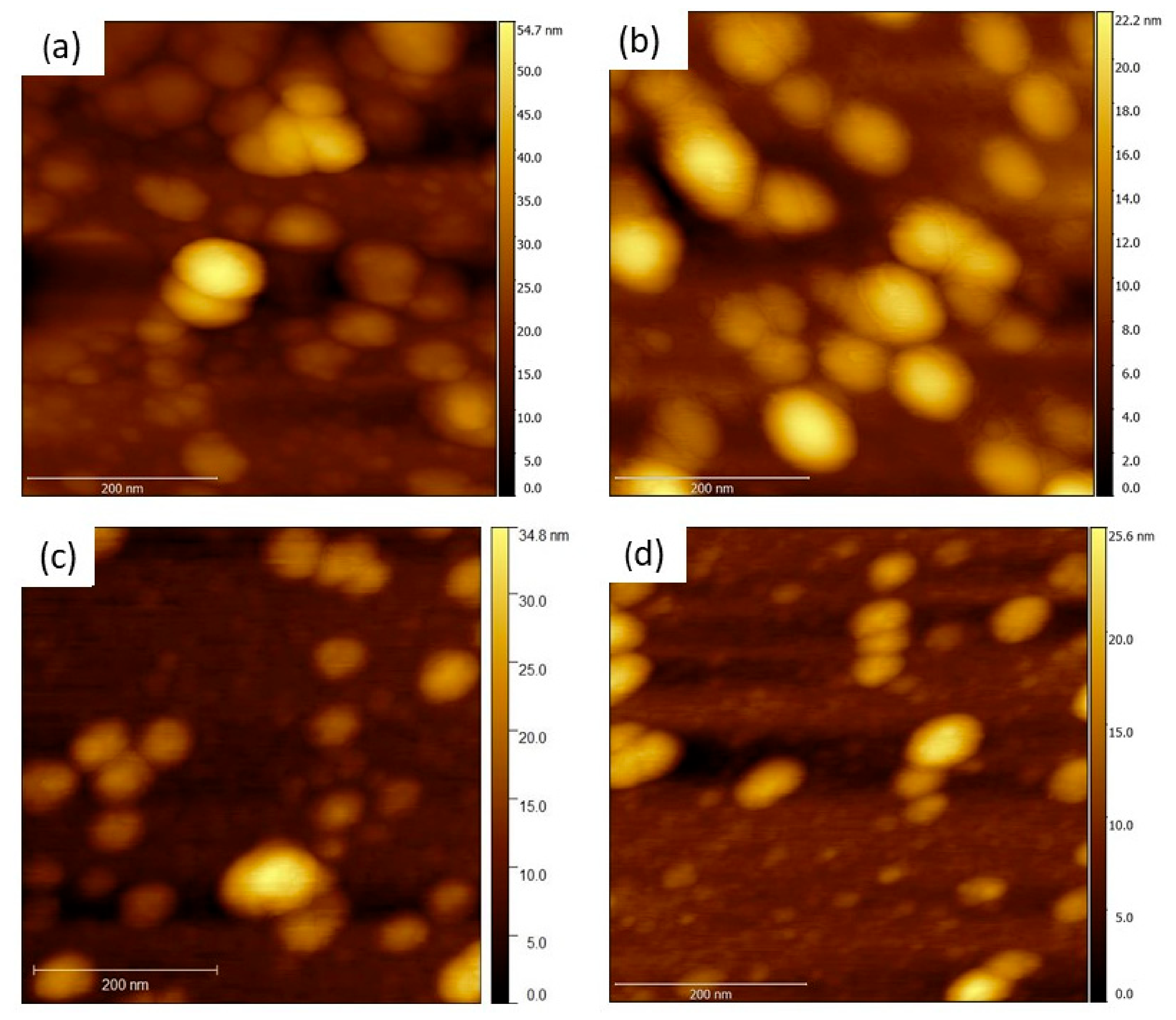
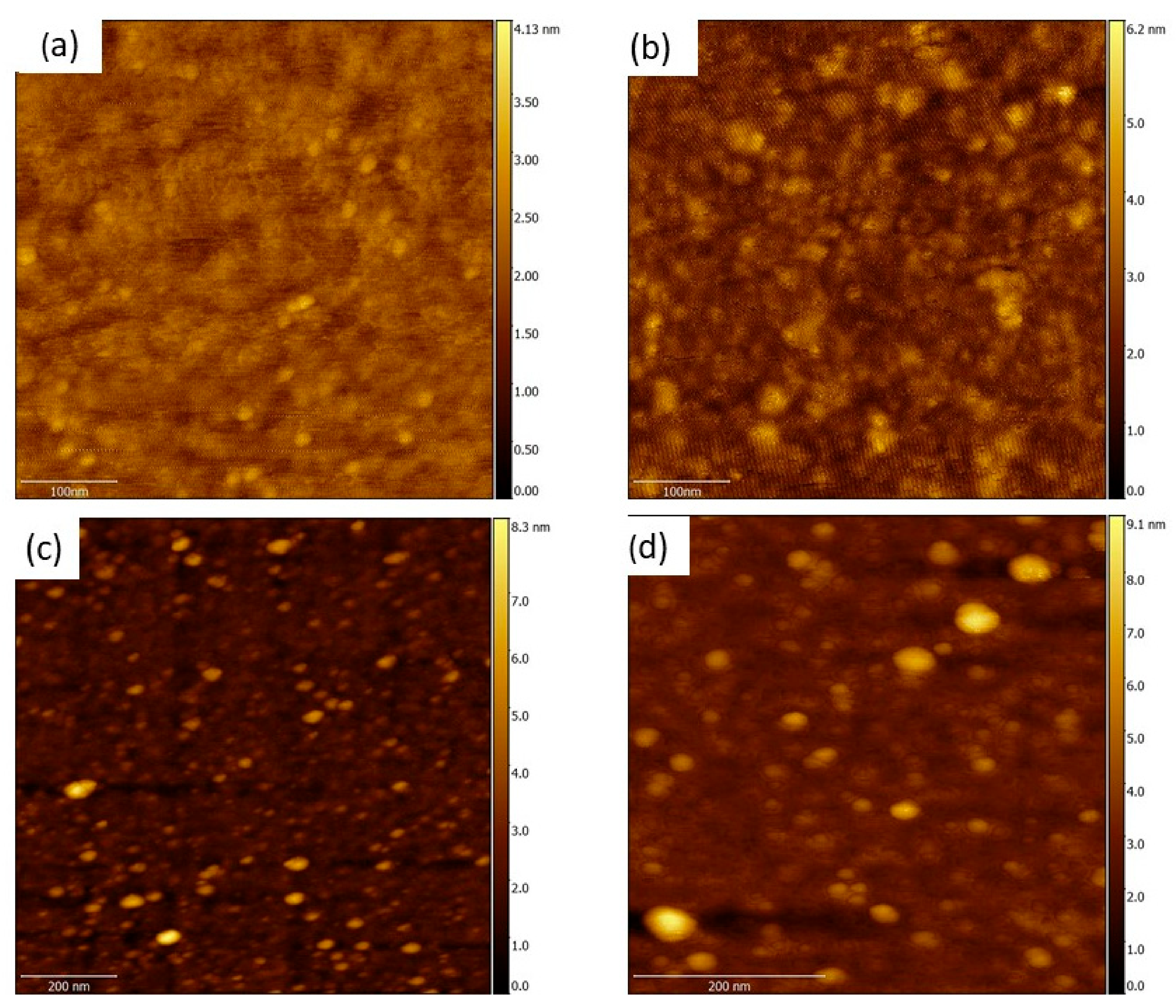
The morphology of the layers was investigated with SEM (
Figure 1) and AFM (
Figure 2 and
Figure 3). According to these, the films are not smooth at an atomic level. They have a slightly granular surface structure with typical grain sizes between 60 and 100 nm. However, all the layers are very smooth, with RMS roughness below 9 nm in the case of silicon substrates and 1 nm on sapphire.
It can be seen from the AFM measurement that all the films are continuous. The grain sizes on Si substrates are around 60 to 100 nm, but the height of the grains is below 30 nm. This results in a low RMS roughness, as
Table 2 shows. The films on the sapphire show a different morphology: They are smoother, and the grain sizes are smaller as well, below 50 nm in all cases. A roughening of the samples after annealing is generally expected due to aggregation and crystallization of the layer resulting in the growth of the grain size. This expected effect can be seen in the samples deposited at 200 °C and the one deposited at 300 °C on sapphire, where the RMS roughness calculated from the AFM images increases. The layer deposited on Si at 300 °C shows a decreased RMS roughness after annealing, but this is the result of smoothening of the smaller grained areas, whereas the larger (~100 nm) grains increase after annealing. Therefore, recrystallization can take place in this case as well.
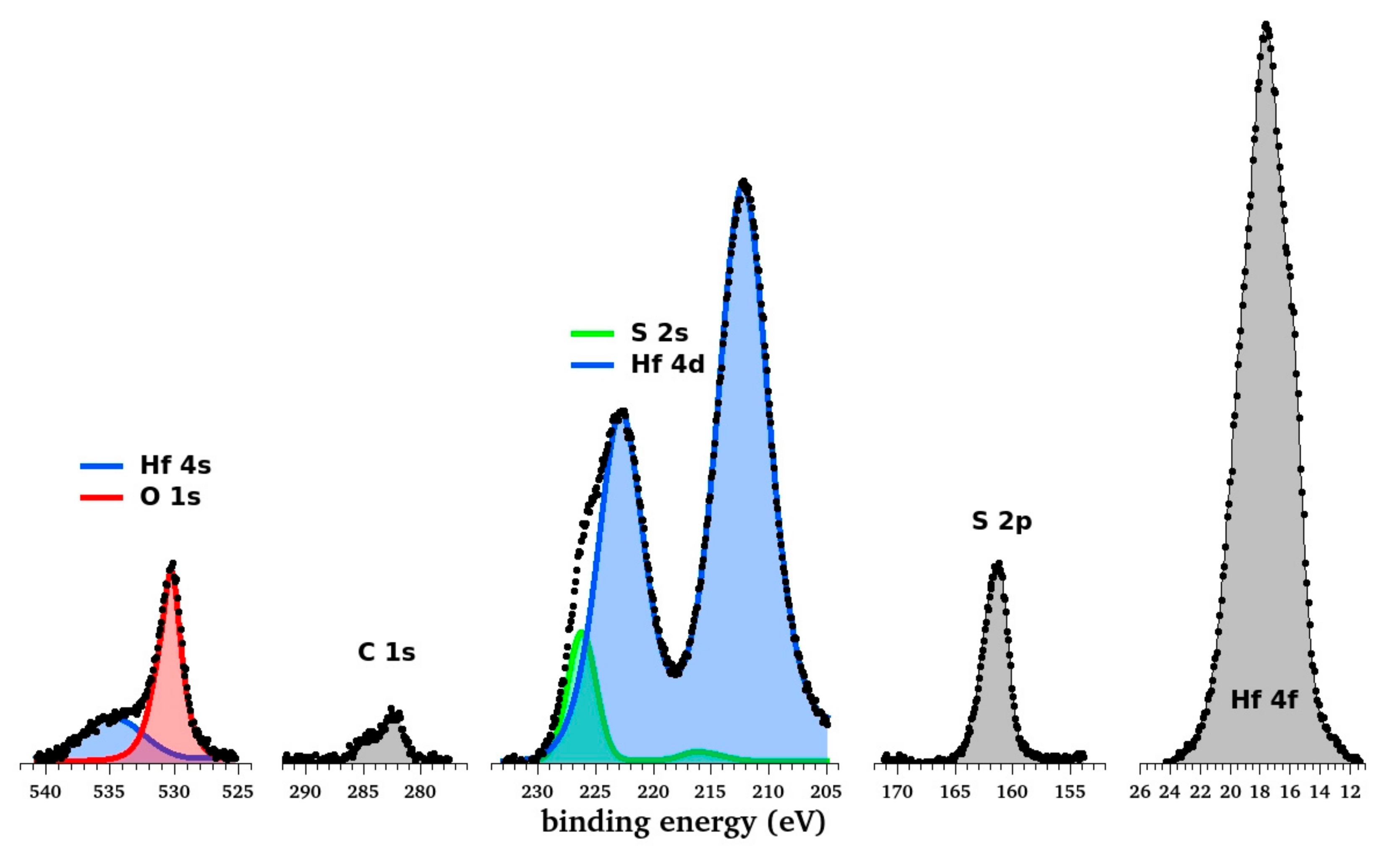
The composition of the deposited layers was determined by XPS. Since XPS detects and provides information from the range of a few nm and the top surface is presumably oxidized and somewhat contaminated, a depth profile of composition was measured. The spectra were detected with an alternating ion sputtering and measurement of the HfS
2 layer. The applied ion sputtering was regarded as not influencing the atomic composition. A typical spectrum is shown in
Figure 4. The black dots show the detected spectrum. Color lines show the fitted component peaks. Component fitting was necessary because the oxygen peak (530 eV) is in the vicinity of the Hf 4s peak, and thus, some overlapping occurs. A similar coincidence is visible at 225 eV, where the sulfur 2s peak overlaps the hafnium 4d 3/2 peak.
The Hf 4f peak seems to be a single wide peak, whereas, in reality, it is a sum of 4 subpeaks because the 4f doublet (5/2 and 4f 7/2) peaks are shifted differently for Hf-sulfide and Hf-oxide. The close vicinity of the 4 subpeaks prevents their separation in the spectra measured by this equipment. However, the shape of their sum shows that hafnium atoms are bound partially to oxygen and partially to sulfur.
The spectra were evaluated using a homogeneous model and yielded a concentration distribution shown in
Figure 5a. Both Hf peaks (Hf 4d 5/2 and Hf 4f) were evaluated, and they resulted in the same composition within 2%.
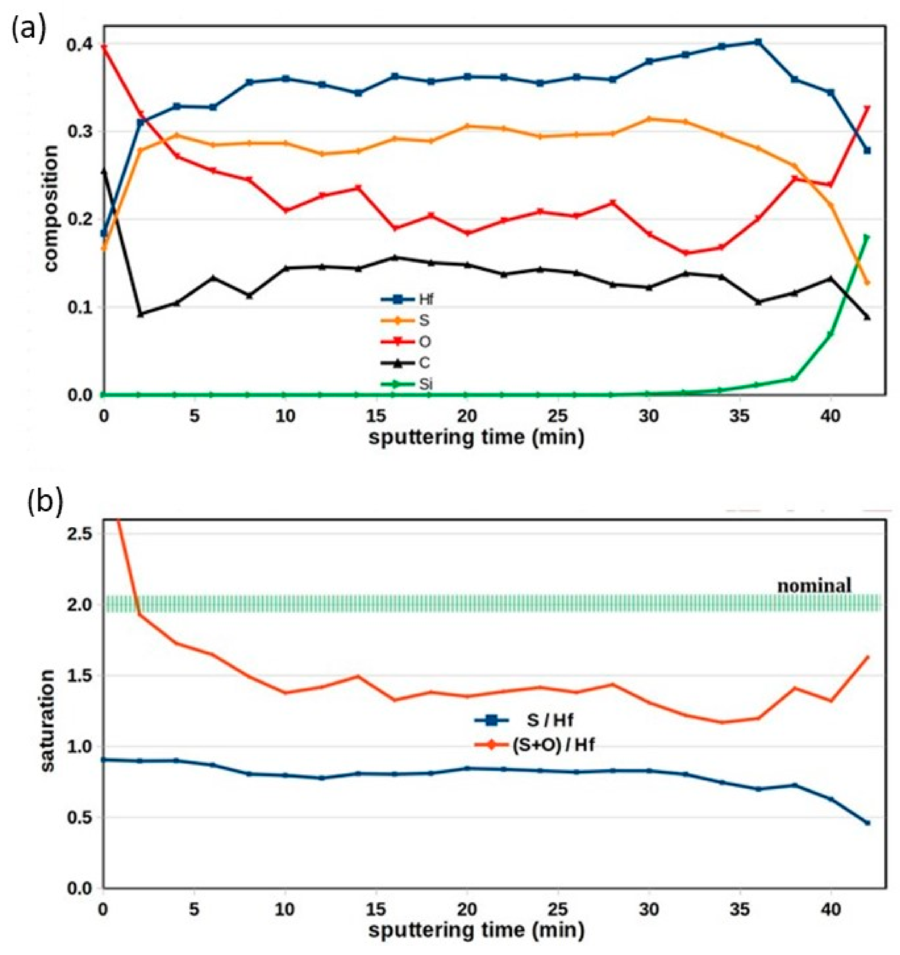
Figure 5 shows the results derived from the Hf 4d peak. The profile shows the elemental distribution from the surface (at zero sputtering time) down to the SiO
2 substrate (at 40 min). We can conclude the following from the depth profile:
- -
The surface contamination is limited to the topmost atomic layer, and no extra carbon penetrated into the layer from the surface after deposition, but there is a built-in carbon content (~13%) in the film.
- -
Oxidation took place after layer deposition, which resulted in increased oxygen content in the surface region (0–10 min in the figure).
- -
The HfS2 layer is not pure sulfide, but instead a mixture of oxide and sulfide. Though the sulfur concentration (~30 at%) well exceeds the oxygen concentration (~20 atom%), the film is not pure HfS2.
- -
The oxygen and sulfur combined amount (~50 at%) does not reach the value attributed to a saturated Hf oxide or sulfide compound or a mixture of the two (which would be ~70 at%).
The atomic ratios are presented in a separate graph in
Figure 5b. The sulfur/hafnium ratio is constant along with the layer thickness (blue line). The combined (oxygen + sulfur)/hafnium ratio, which refers to the saturation level of HfO
2 or HfS
2 compounds, is presented by the red line. According to the oxygen penetration mentioned above, this combined ratio changes along with the layer thickness. However, it is almost stable inside the layer. Its value of 1.45 is not close to the nominal value of 2.0 (green band).
The occurrence of oxidation during the deposition of HfS
2 layers is a problem encountered by all research. Most papers report the presence of some HfO
2 in the prepared films. Mattinen et al. found around a 5% oxygen ratio in the films deposited at over 400 °C, despite every effort of eliminating residual oxygen from the reactor [
21], while Chang et al. [
22] found between 37 and 50% oxygen content. It appears that the present work does not solve this problem either but presents proof of the preparation of crystalline HfS
2, contaminated with some HfO
2.
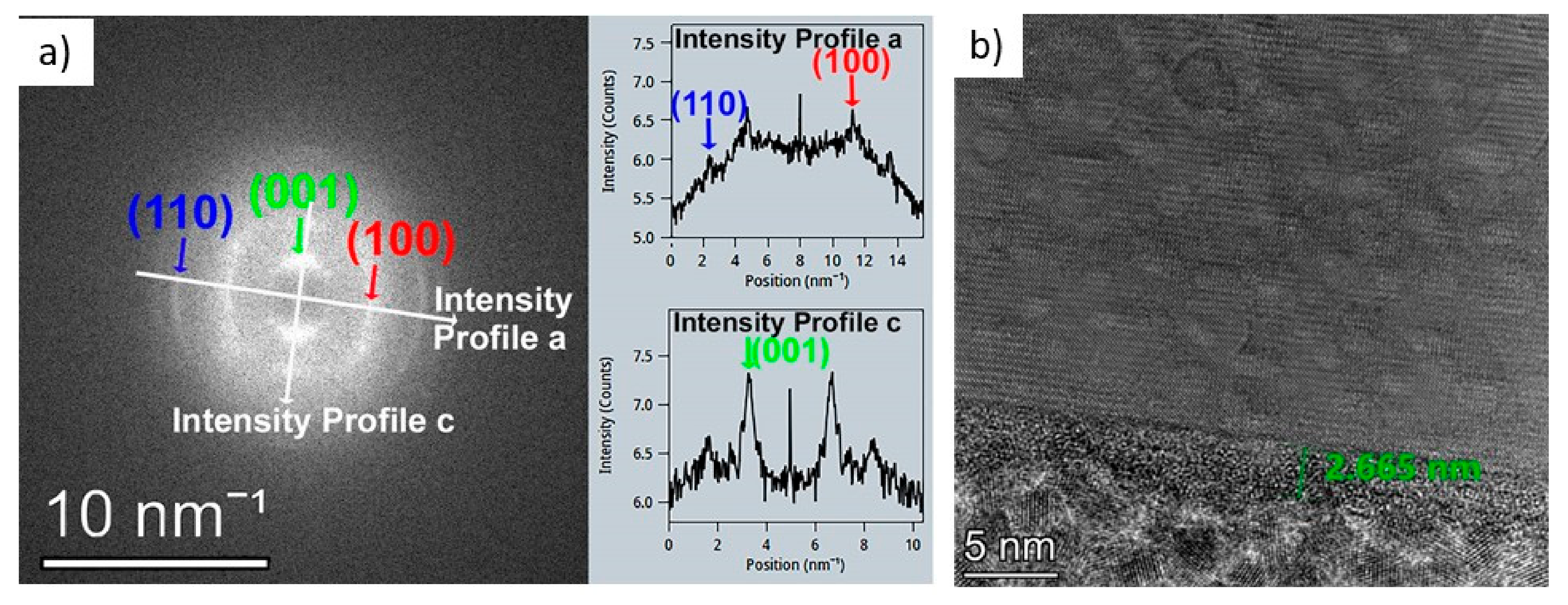
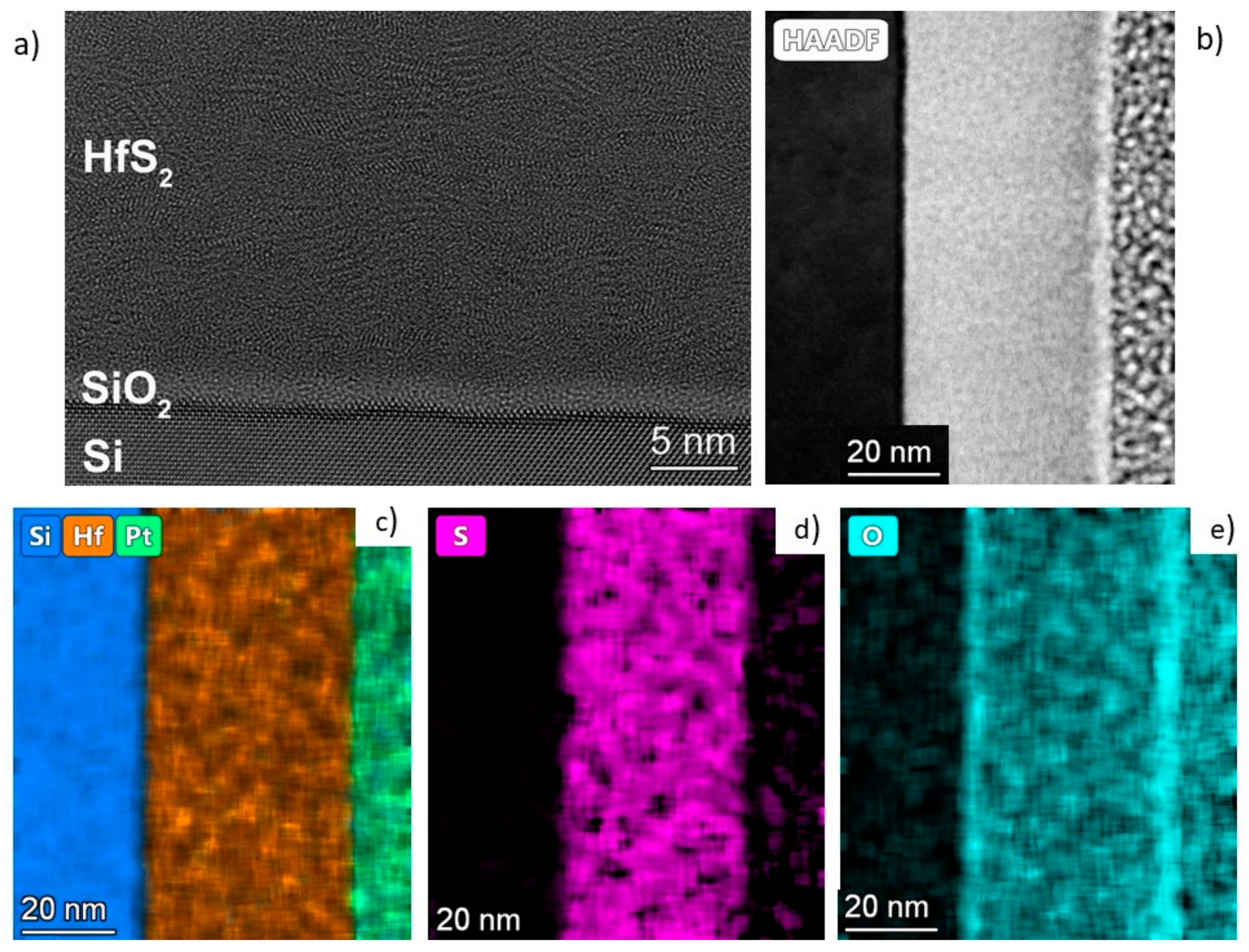
The structure of the layers was further explored with TEM measurements (see
Figure 6 and
Figure 7). The FFT analysis of the film deposited at 300 °C and annealed at 400 °C can be seen in
Figure 6a. The annealed layer consists of crystalline 2D HfS
2 films stacked upon each other with an average distance of 0.59 nm between them. This distance is in good agreement with the lattice distance of HfS
2 (001). The (001) planes of HfS
2 are, on average, parallel to the surface of the substrate, but this is only true with a very heavy grip. This strong scattering is shown by the smeared (001) peak in
Figure 6b and the corrugated HfS
2 layers in
Figure 6a. Most of the layer is crystalline, but due to the wavy and intermittent HfS
2 layers, it is difficult to rule out the presence of an amorphous phase between the sections of the HfS
2 layers. A few nm amorphous layers can be observed on the surface of the deposited layers. This amorphization is due to the oxidation based on the EDS investigations in
Figure 7. As can also be seen from the elemental mapping (
Figure 7), the layers contain some oxygen, though mostly in the surface areas. The measurement showed no crystalline HfO
2 present. The minor oxygen contamination is mostly present at the surface.
After the thicker films, an ultra-thin layer was also synthesized. For this purpose, ten ALD cycles were performed, with three times longer TDMAH pulses followed by the closure of the ALD reactor for 1.5 s, then the evacuation of the reaction chamber was closed down for 6 s to ensure enough time for the precursors to chemisorb to the surface and react with one another (picoflow mode). This method ensures that this ultra-thin film is also continuous and uniform. The thickness of the resulting thin film was measured by AFM (after etching a step with buffered oxide etchant in the layer), and it was found to be 2.6 nm. This means that the resulting film was about 5–6 monolayers thick (
Figure 6b).
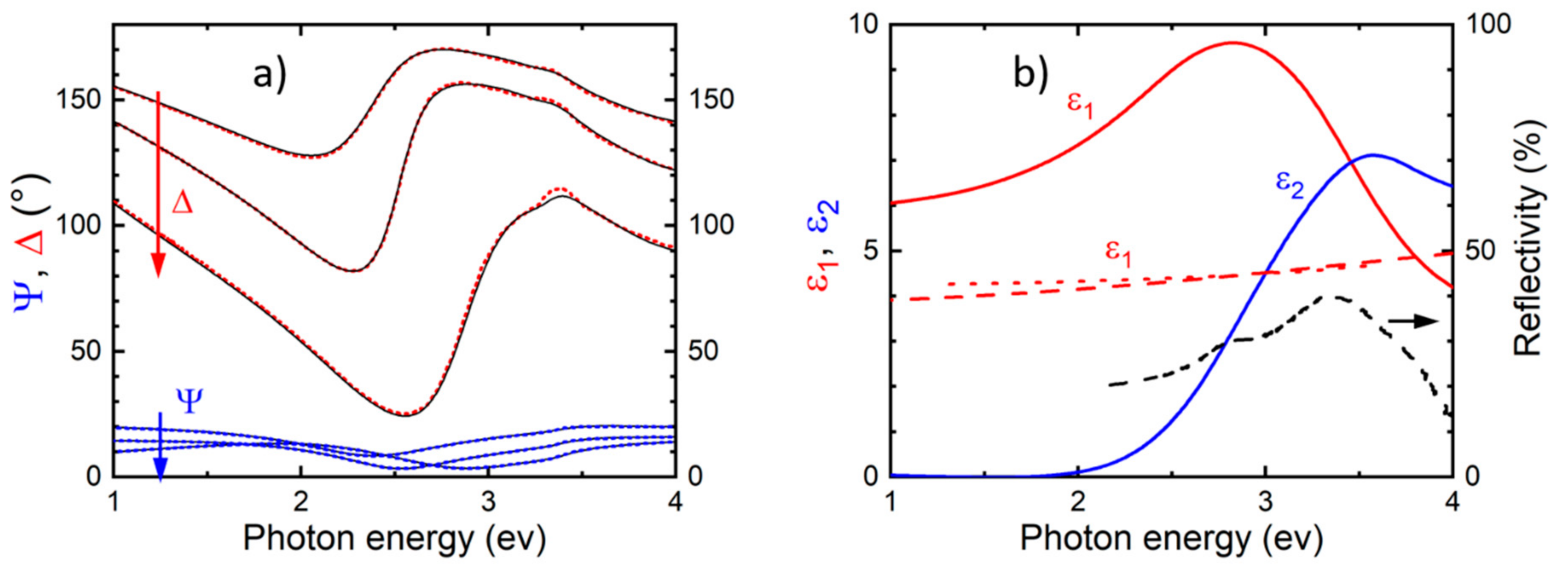
The dielectric function spectra of the as-deposited films on Si measured by SE also reveal an amorphous structure. The imaginary part of the dielectric function (ε
2) shows a broad absorption peak around the E
1 and E
2 electronic transition energies (
Figure 8), the positions of which are clearly visible on the reflectivity measurement on crystalline HfS
2 [
26]. The SE measurements revealed high-quality, dense, compact, and homogeneous layers with a thickness of ≈40 nm. The optical band gaps of the layers were also calculated from the SE data. The gap of the film deposited at 200 °C was 2.2 eV, and that of the film deposited at 300 °C was higher, 3.3 eV. The film deposited at 400 °C showed no definable band gap and instead appeared to present dielectric properties. This suggested a HfO
2-like behavior and implied that the layer might be partly or completely oxidized. Therefore, this film was further investigated.
Deposition at 400 °C
The films deposited at 400 °C showed completely different properties from the previous ones (
Figure S1). The growth rate was somewhat lower, 0.06 nm/cycle at this temperature, which shows that the ALD window for the deposition of HfS
2 material has already been surpassed. The resulting layers were just as homogeneous as the previous ones, with an RMS roughness of 1.77 nm (on sapphire).
As the SE suggested an oxide-like composition, the film was investigated by XPS too. As this layer was a much thinner one (due to the lower growth per cycle), the depth profile only consisted of three steps: the surface, the medium part of the layer and the interface to the wafer. These three measurements are not fully independent; the depth range overlaps with each other since the total observed range of photoelectrons is ~10 nm. The surface spectrum showed a HfO2-like composition with some extra features. Accordingly, the Hf 4f twin peaks are presented in a clear doublet form typical of Hf-oxide. In this spectrum, the carbon content of the layer cannot be distinguished from the carbon diffused after the deposition, and it had an enhanced carbon concentration. The Si substrate also yielded some contributions to this spectrum.
The most significant spectrum is the one from the middle of the layer. The contribution of the Si wafer to the spectrum, as well as the Si 2p peaks corresponding to elemental and oxide silicon and the oxygen peaks attributed to Si-oxide, were removed from the measured values resulting in values shown in
Table 3.
The carbon may be over-detected if we assume that the surface contamination was not fully removed. The hafnium 4d peak showed a smaller distortion due to the presence of a sulfide peak but is still dominantly an oxide shape. The observed sulfur is the actual physical quantity. However, it needs to be corrected according to the 3rd spectrum, which revealed that the wafer interface had an increased sulfur content. Though the accurate subtraction of the interface contribution to the observed sulfur cannot be carried out, an estimated sulfur concentration can be given for the layer composition. It is shown in
Table 3. Additionally, it needs to be noted that the sulfur peak observed in this layer originated from oxygen-bound sulfur atoms (sulfite or sulfate). This differs from the layer prepared at 300 °C, where the sulfur content was in a sulfide state. This can be explained by the oxidation of the sulfur due to the high oxygen content.
It is clear from these results that the growth at 400 °C is already outside of the ALD window of HfS2 growth, and instead of forming sulfides, at this temperature, the residual oxygen in the reaction chamber and provided by the purging nitrogen gas (although 6N purity nitrogen in our case) reacts with the precursor, forming HfO2 somewhat contaminated with sulfates. However, this may also be an interesting result from a technological point of view. As the preparation of HfO2 is always cumbersome, and the resulting films are rarely uniform and always granular in structure, this technique can result in superior insulating films. The resistivity of the layer was measured with a four-point probe, and its insulating properties were as good as that of HfO2, but the uniformity and smoothness of the layer exceeded those of HfO2.


