
Conception of High-Frequency Power Planar Transformer Prototypes Based on FabLab Platform

 ,
,
Abstract
:1. Introduction
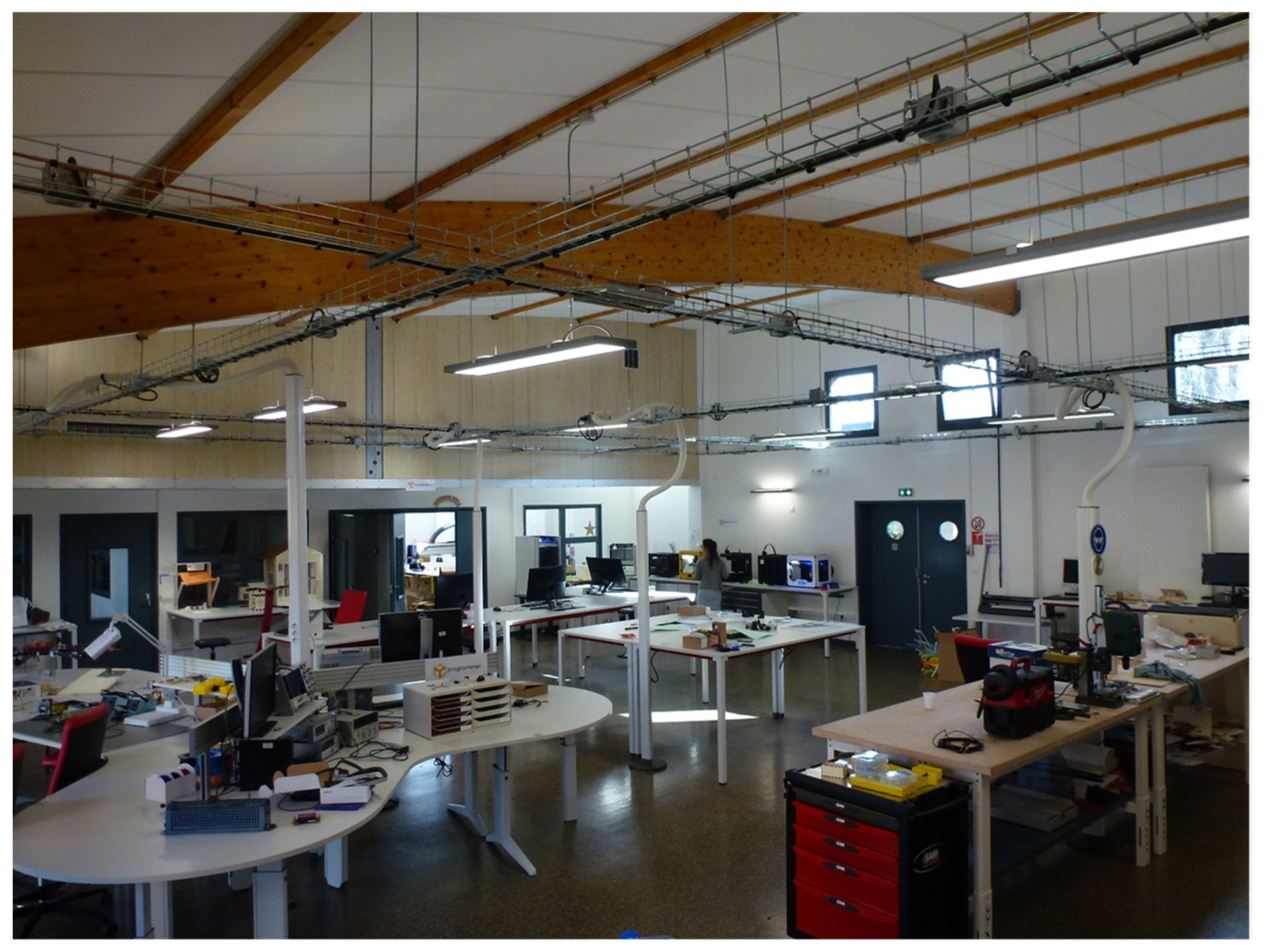
2. FabLab
3. Technological Considerations for the High-Frequency (HF) Planar Transformer Prototype
3.1. Conceiving Planar Transformer: Printed Circuit Board (PCB) vs. Copper Foil
- Copper track thicknesses are not limited. Bigger conductors can be selected in order to limit or at least reduce complex paralleling layers with respect to skin depth that is problematic. Moreover, primary and secondary thicknesses can easily be set to different values.
- Distance between layers can also be set to different values, stacking insulated layers. Insulation material can also be chosen differently according to layers.
- Leakage values can be increased by spacing primary and secondary windings or by introducing ferrite polymer composite (FPC) material between layers, like C350 for example [31].
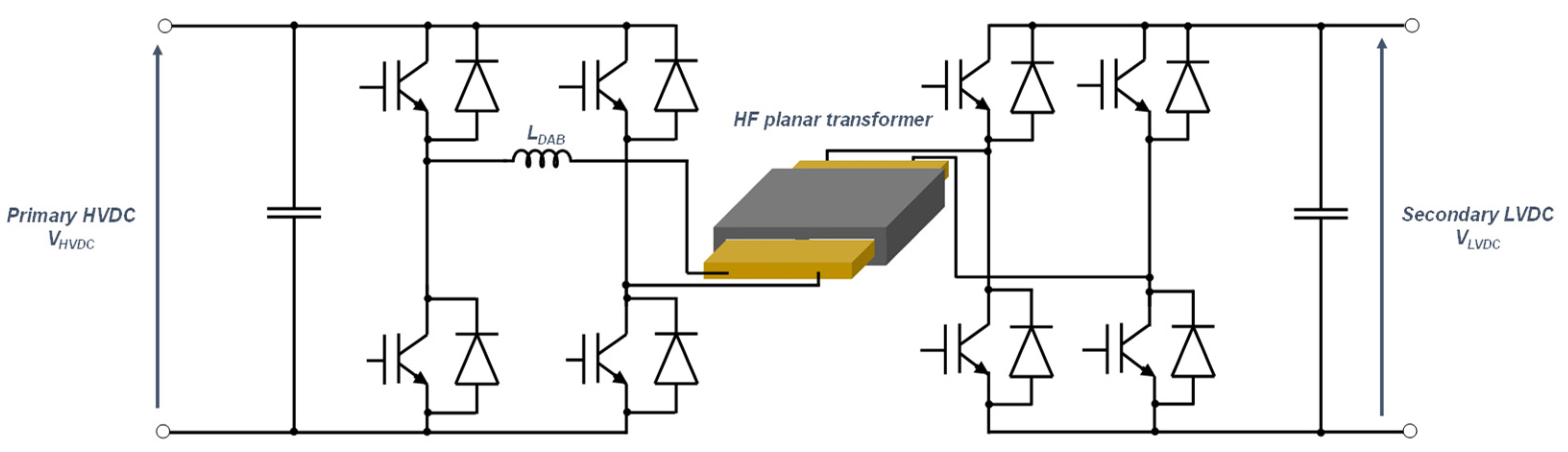
3.2. Transformer Prototype Specifications
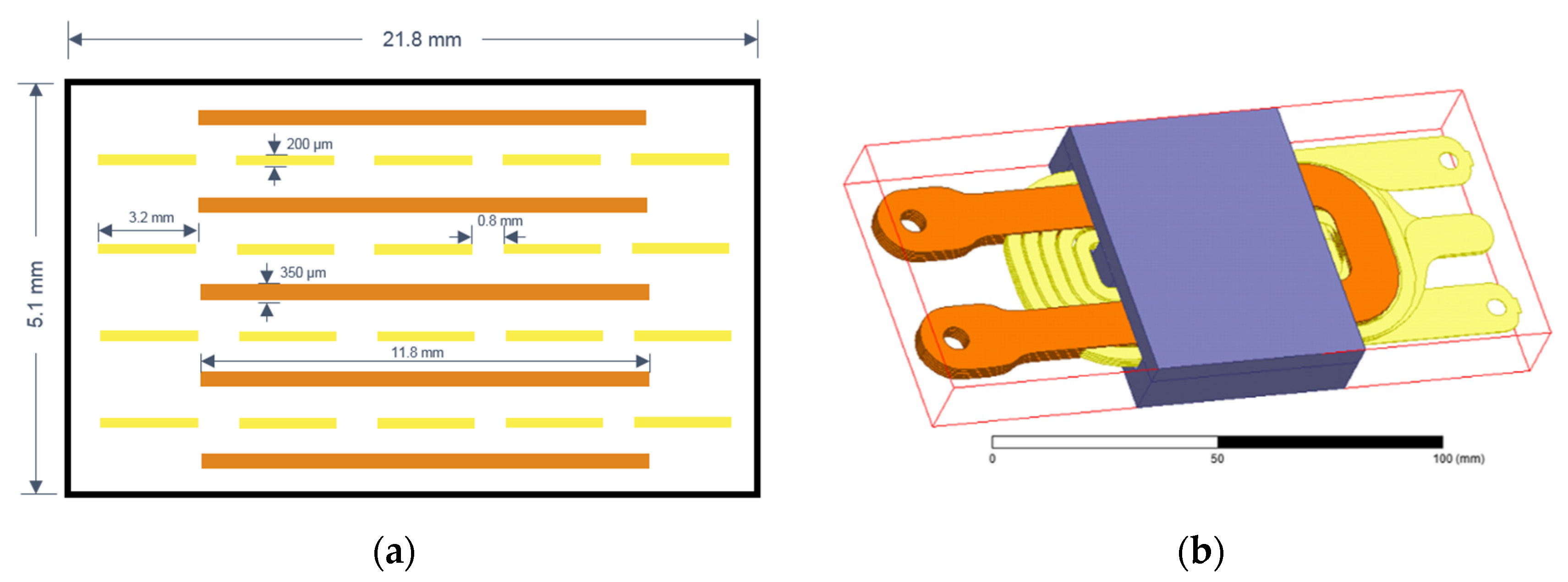
3.3. Transformer Design and Description
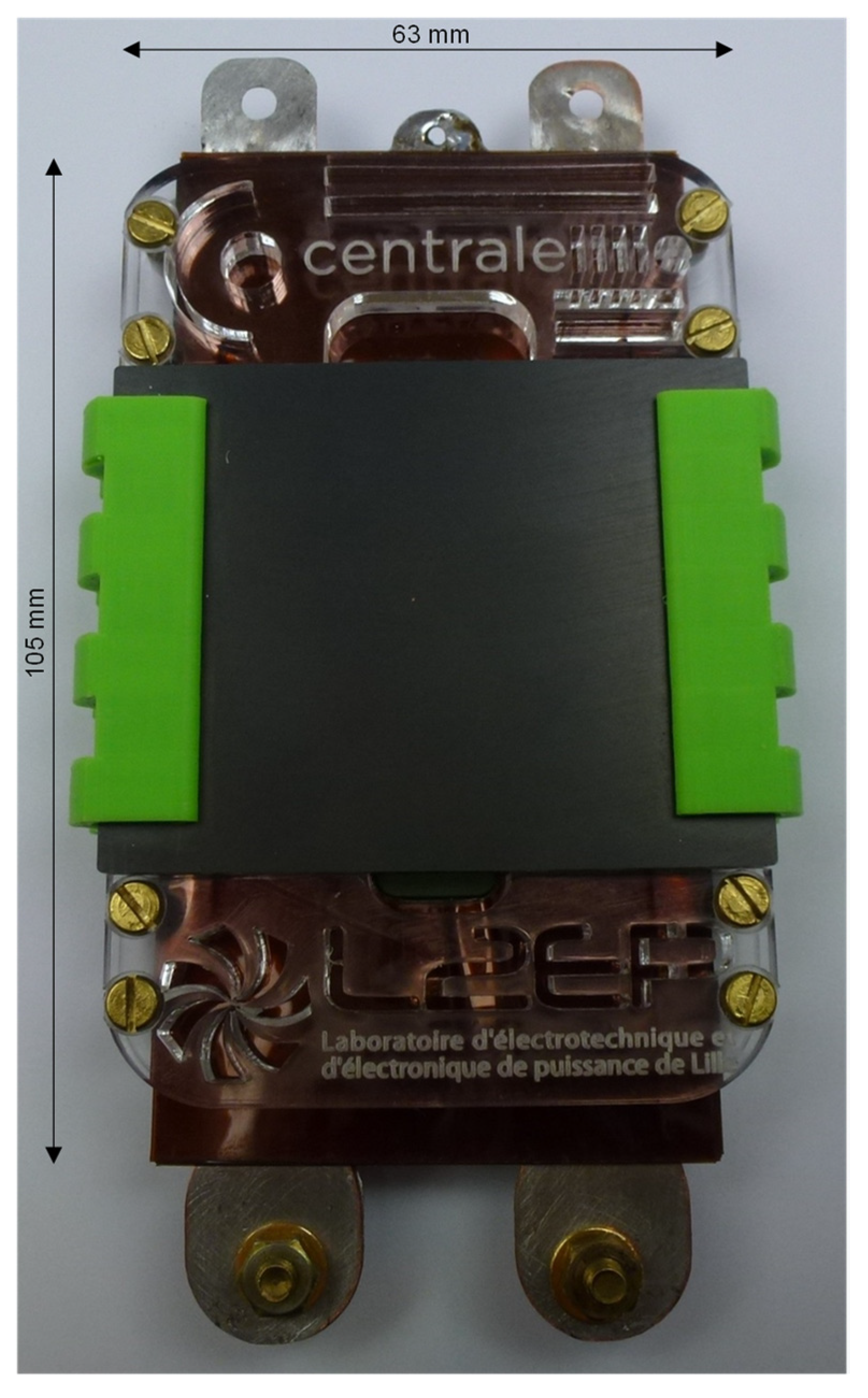
4. Prototype Achievement in FabLab Environment
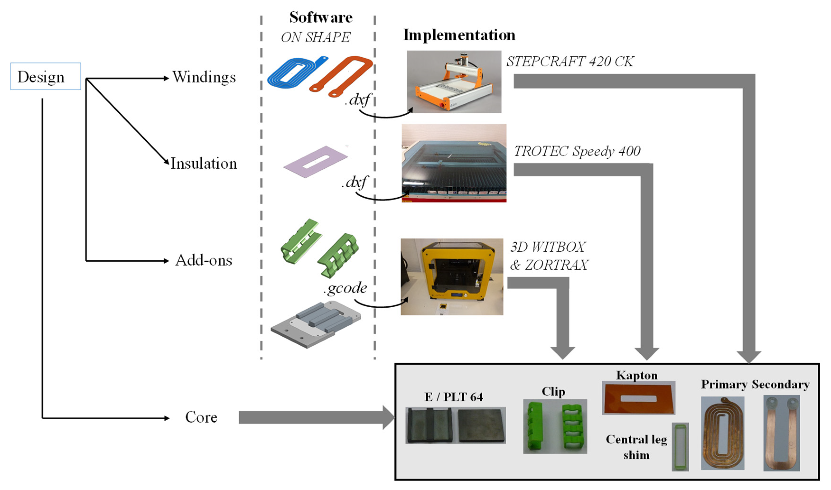
4.1. Manufacturing Process Overview
4.2. Parts Production
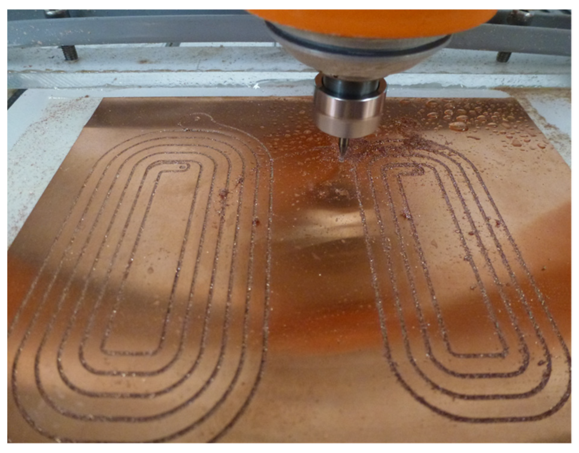
- Copper windings: after their shape design, primary and secondary winding copper tracks are carved using a computer numerical control (CNC) machine Stepcraft 420 CK [42]. Figure 5 shows the milling process for two primary layers. During this process, lubricant is sprayed regularly. This provides two benefits: the drill run cooler and copper filings do not hang up. As a consequence, the drill’s lifetime is extended. Then, endpoints of copper tracks are tined to ease connections between layers. Finally, winding layers are ready for assembling. One can note that all the secondary tracks are identical due to the parallel winding. On the opposite, primary layers are different in order to make possible series connections between the layers.
- Kapton insulation: insulation between layers is made with Kapton film. Elementary 75 µm Kapton layers are then cut using the laser cutting machine Trotec Speedy 400 [43] to consider magnetic core and central leg size. Distances between winding layers will be set adding more or less of these elementary layers.
- Add-ons: in order to assemble the transformer prototype, some supplementary elements have to be developed. Firstly, plexiglass clamps and secondary winding centering pins have to be cut with the laser cutting machine. All these elements are made of polymethyl methacrylate (PMMA) material. Secondly, clips and central leg shim are printed in 3-D [44]. They are made of polylactic acid (PLA) material. Clips are used for maintaining both magnetic core parts together while the central leg shim is used for centering and spacing primary winding from the central core leg.
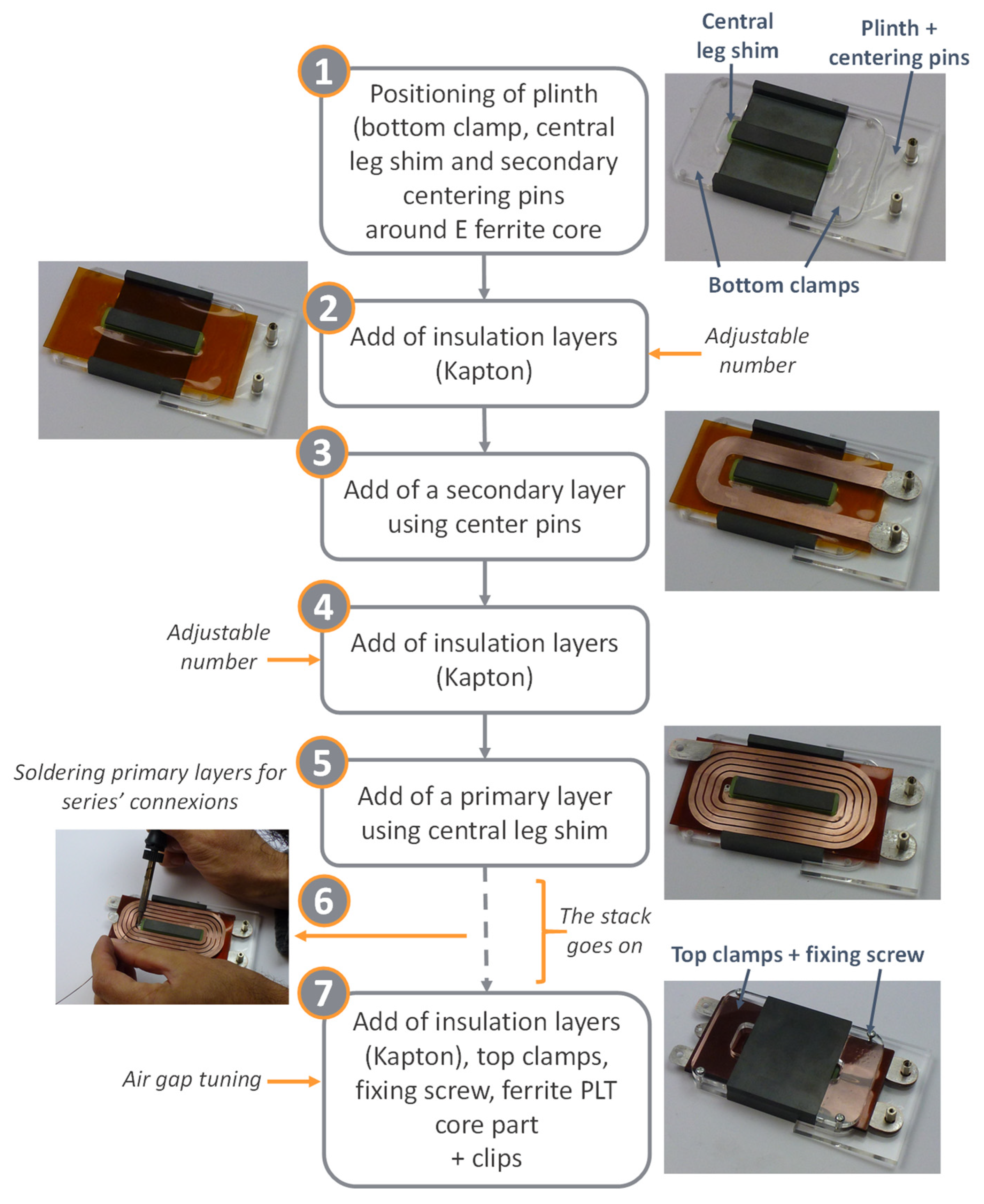
4.3. Assembly Operations
- Step 1: The plinth, including bottom clamps and centering pins is set around the E-part core.
- Step 2: Kapton insulated layers are added. Insulating thickness is adjusted adding more or less elementary layers.
- Step 3: First secondary layer is positioned using centering pins.
- Step 4: Kapton layers are added.
- Step 5: First primary winding is added. As can be seen in Figure 6, primary pins are located on the opposite side of the secondary winding. The biggest one corresponds to the winding connecting pin, while the smallest one, located close to the ferrite core, is used for connecting this layer to the next one. The primary winding’s centering is ensured by the central leg shim that locks its positioning.
- Step 6: Stacking takes place, interleaving insulating layers, secondary winding layers and primary layers, respecting the layout introduced in Figure 3a. During this step, primary winding layers have to be soldered for setting the 20 turns of the winding.
- Step 7: When the last secondary layer is added, the stacking is almost over. Some insulated layers are inserted before the magnetic core to be closed with the ferrite PLT core part. The air gap is tuned adding some Kapton between E and PLT core parts. Then, the upper side of the plexiglass clamps is screwed to the bottom one to fix layers’ stack. Clips are tightened around the magnetic core while the plinth with centering pins is removed.
5. Prototype Validation: Characterization and Tests
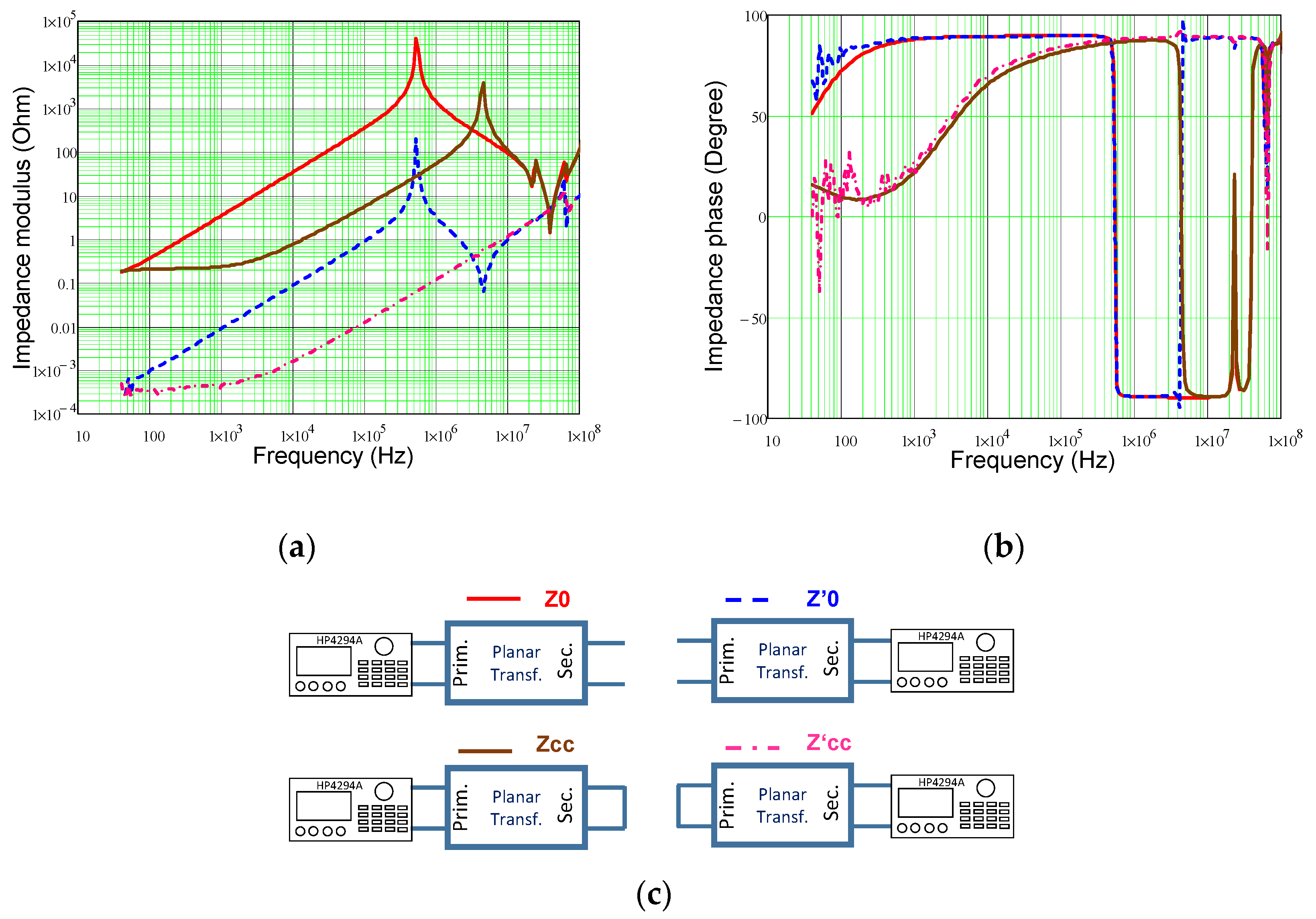
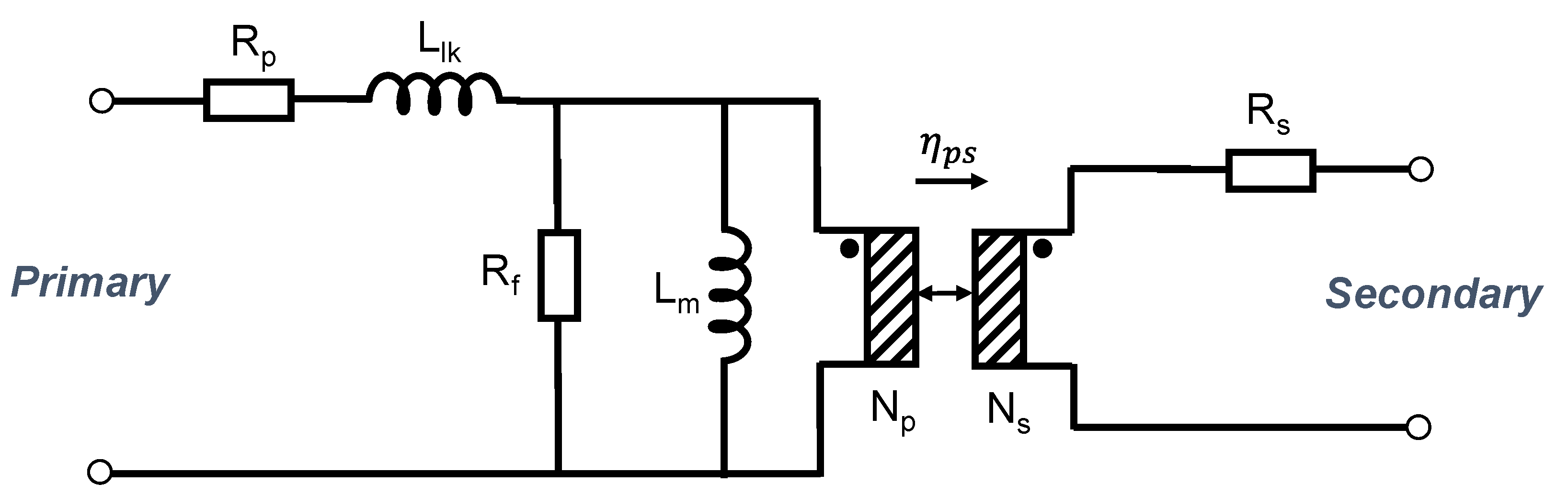
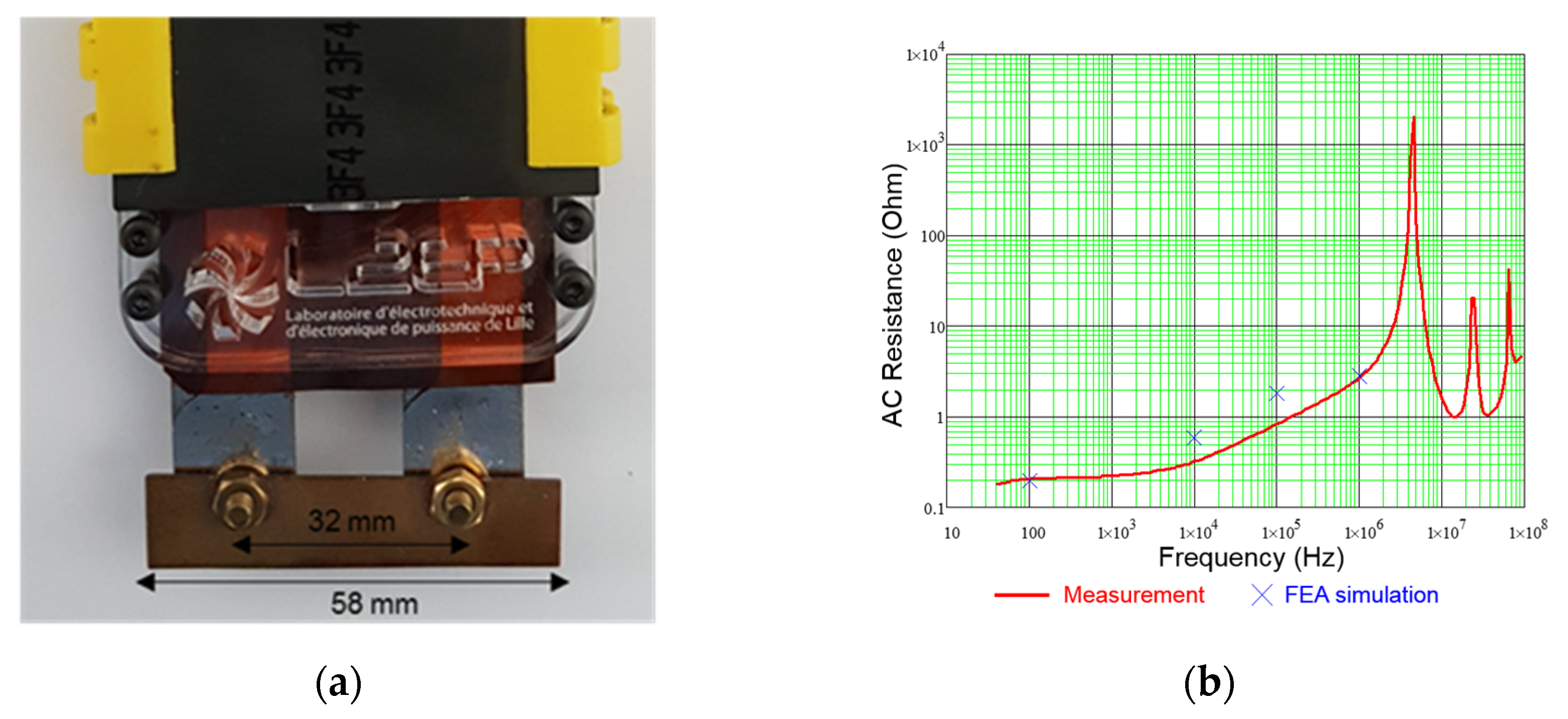
5.1. Small Signal Characterization Based on Impedance Measurements
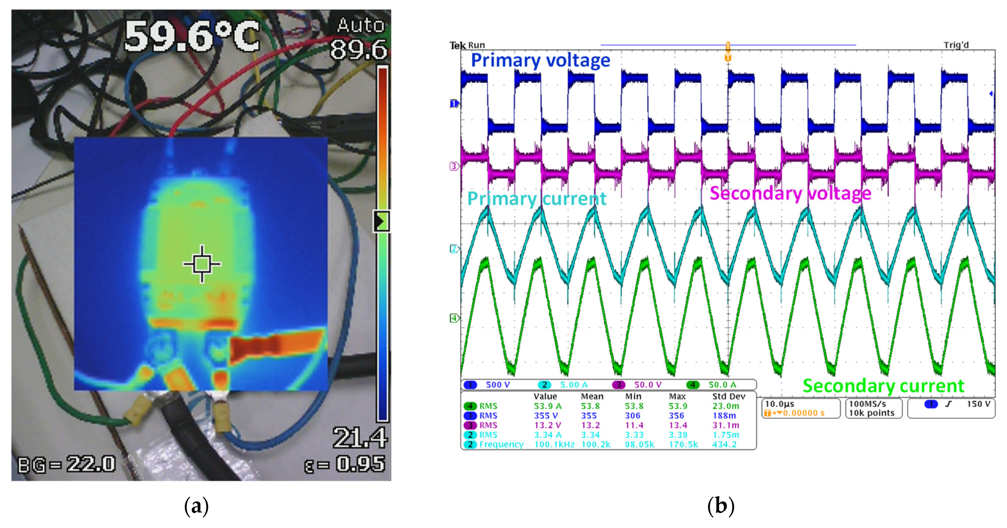
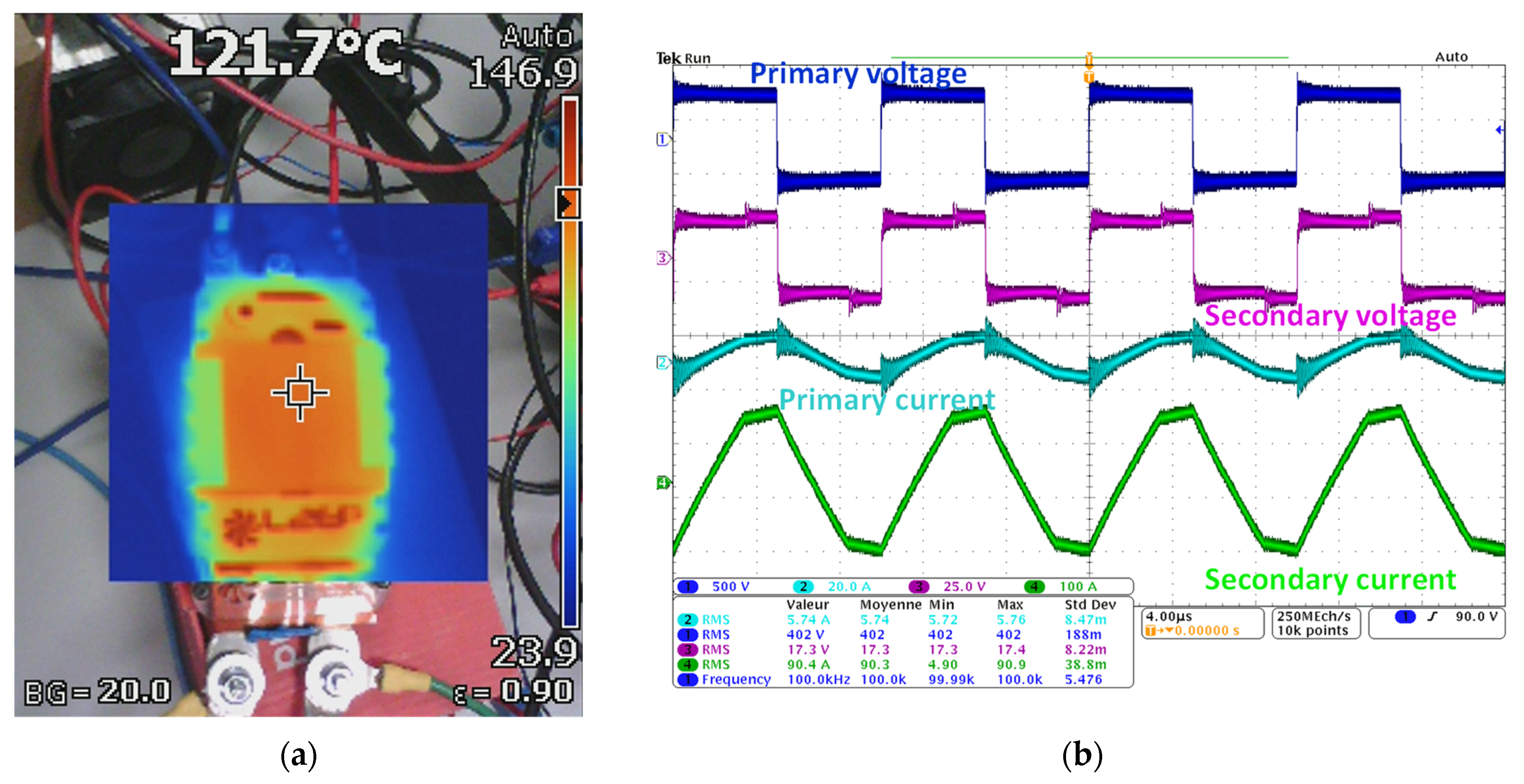
5.2. Thermal Characterization with Open and Short Circuit Power Measurements
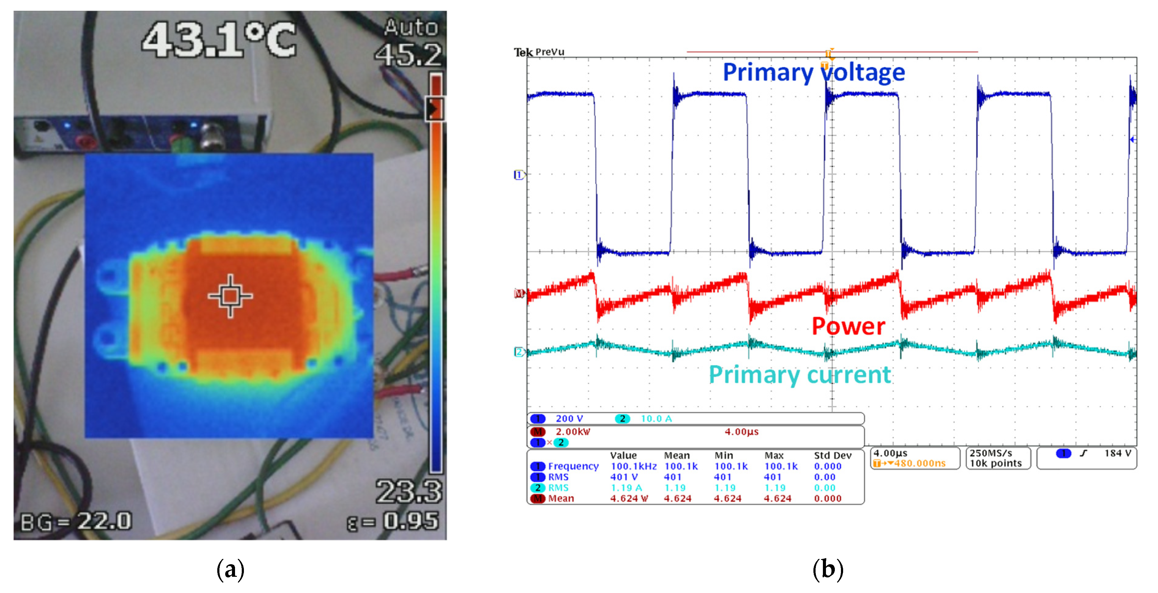
5.2.1. Open Circuit Test
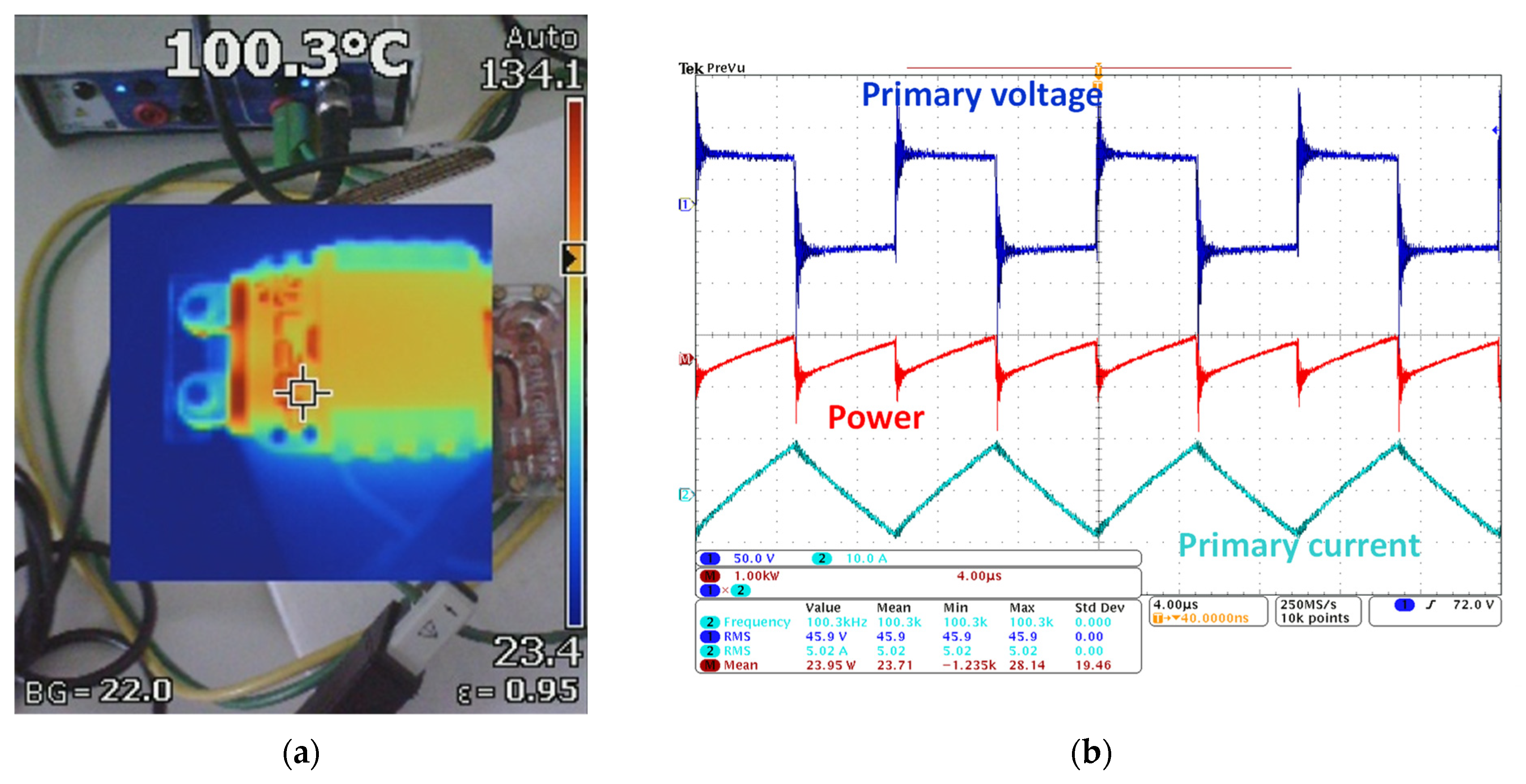
5.2.2. Short-Circuit Test
5.2.3. Load Tests
5.3. Comments on Measurements and Process
6. Conclusions
Author Contributions
Funding
Institutional Review Board Statement
Informed Consent Statement
Data Availability Statement
Conflicts of Interest
References
- Quirke, M.T.; Barrett, J.J.; Hayes, M. Planar magnetic component technology-a review. IEEE Trans.Compon. Hybrids Manuf. Technol. 1992, 15, 884–892. [Google Scholar] [CrossRef]
- Ouyang, Z.; Andersen, M.A.E. Overview of Planar Magnetic Technology–Fundamental Properties. IEEE Trans. Power Electron. 2014, 29, 4888–4900. [Google Scholar] [CrossRef]
- Ngoua, T.; Magambo, J.S.; Bakri, R.; Margueron, X.; Le Moigne, P.; Mahe, A.; Guguen, S.; Bensalah, T. Planar Magnetic Components in More Electric Aircraft: Review of Technology and Key Parameters for DC-DC Power Electronic Converter. IEEE Trans. Transp. Electrif. 2017, 3, 831–842. [Google Scholar] [CrossRef]
- Betts, B. Bringing the factory home [Manufacturing Personal]. Eng. Technol. 2010, 5, 56–58. [Google Scholar] [CrossRef]
- Redlich, T.; Buxbaum-Conradi, S.; Basmer-Birkenfeld, S.-V.; Moritz, M.; Krenz, P.; Osunyomi, B.D.; Wulfsberg, J.P.; Heubischl, S. OpenLabs—Open Source Microfactories Enhancing the FabLab Idea. In Proceedings of the 2016 49th Hawaii International Conference on System Sciences (HICSS), Koloa, HI, USA, 5–8 January 2016; pp. 707–715. [Google Scholar] [CrossRef]
- Fiaidhi, J.; Mohammed, S. Fab Labs: A Platform for Innovation and Extreme Automation. IT Prof. 2018, 20, 83–90. [Google Scholar] [CrossRef]
- Stephenson, M.K.; Dow, D.E. The community FabLab platform: Applications and implications in biomedical engineering. In Proceedings of the 2014 36th Annual International Conference of the IEEE Engineering in Medicine and Biology Society, Chicago, IL, USA, 26–30 August 2014; pp. 1821–1825. [Google Scholar] [CrossRef]
- Angrisani, L.; Arpaia, P.; Bonavolonta, F.; Lo Moriello, R.S. Academic FabLabs for industry 4.0: Experience at University of Naples Federico II. IEEE Instrum. Meas. Mag. 2018, 21, 6–13. [Google Scholar] [CrossRef]
- Gendreau, D.; Mohand-Ousaid, A.; Rougeot, P.; Rakotondrabe, M. 3D-Printing: A promising technology to design three-dimensional microsystems. In Proceedings of the 2016 International Conference on Manipulation, Automation and Robotics at Small Scales (MARSS), Paris, France, 18–22 July 2016; pp. 1–5. [Google Scholar] [CrossRef]
- Lim, C.W.J.; Le, K.Q.; Lu, Q.; Wong, C.H. An Overview of 3-D Printing in Manufacturing, Aerospace, and Automotive Industries. IEEE Potentials 2016, 35, 18–22. [Google Scholar] [CrossRef]
- Dahle, R.; Rasel, R. 3-D Printing as an Effective Educational Tool for MEMS Design and Fabrication. IEEE Trans. Educ. 2016, 59, 210–215. [Google Scholar] [CrossRef]
- Fiorillo, L.; Leanza, T. Worldwide 3D Printers against the New Coronavirus. Prosthesis 2020, 2, 87–90. [Google Scholar] [CrossRef]
- Tarfaoui, M.; Nachtane, M.; Goda, I.; Qureshi, Y.; Benyahia, H. 3D Printing to Support the Shortage in Personal Protective Equipment Caused by COVID-19 Pandemic. Materials 2020, 13, 3339. [Google Scholar] [CrossRef]
- Rendeki, S.; Nagy, B.; Bene, M.; Pentek, A.; Toth, L.; Szanto, Z.; Told, R.; Maroti, P. An Overview on Personal Protective Equipment (PPE) Fabricated with Additive Manufacturing Technologies in the Era of COVID-19 Pandemic. Polymers 2020, 12, 2703. [Google Scholar] [CrossRef]
- Liang, W.; Raymond, L.; Rivas, J. 3-D-Printed Air-Core Inductors for High-Frequency Power Converters. IEEE Trans. Power Electron. 2016, 31, 52–64. [Google Scholar] [CrossRef]
- Yan, Y.; Ding, C.; Ngo, K.D.T.; Mei, Y.; Lu, G. Additive manufacturing of planar inductor for Power Electronics applications. In Proceedings of the 2016 International Symposium on 3D Power Electronics Integration and Manufacturing (3D-PEIM), Raleigh, NC, USA, 13–15 June 2016; pp. 1–16. [Google Scholar] [CrossRef]
- Simpson, N.; Tighe, C.; Mellor, P. Design of High Performance Shaped Profile Windings for Additive Manufacture. In Proceedings of the 2019 IEEE Energy Conversion Congress and Exposition (ECCE), Baltimore, MD, USA, 29 September–3 October 2019; pp. 761–768. [Google Scholar] [CrossRef]
- Yu, Z.; Yang, X.; Wei, G.; Wang, L.; Wang, K.; Chen, W.; Wei, J. A Novel High-Current Planar Inductor With Cooling Fins Based on 3-D Printing. IEEE Trans. Power Electron. 2021, 36, 12189–12195. [Google Scholar] [CrossRef]
- Hou, T.; Xu, J.; Elkhuizen, W.S.; Wang, C.C.L.; Jiang, J.; Geraedts, J.M.P.; Song, Y. Design of 3D Wireless Power Transfer System Based on 3D Printed Electronics. IEEE Access 2019, 7, 94793–94805. [Google Scholar] [CrossRef]
- Gunewardena, T.R. Manufacturing design considerations for planar magnetics. In Proceedings of the Electrical Insulation Conference and Electrical Manufacturing and Coil Winding Conference, Rosemont, IL, USA, 25 September 1997; pp. 309–311. [Google Scholar] [CrossRef]
- Zumel, P.; Prieto, R.; Cobos, J.A.; Uceda, J. Comparative study of flex-foil technology in HF planar transformer windings. In Proceedings of the 2002 IEEE 33rd Annual IEEE Power Electronics Specialists Conference, Cairns, Australia, 23–27 June 2002; pp. 1248–1253. [Google Scholar] [CrossRef]
- de Jong, E.C.W.; Ferreira, B.J.A.; Bauer, P. Toward the Next Level of PCB Usage in Power Electronic Converters. IEEE Trans. Power Electron. 2008, 23, 3151–3163. [Google Scholar] [CrossRef] [Green Version]
- Saket, M.A.; Shafiei, N.; Ordonez, M. LLC Converters with Planar Transformers: Issues and Mitigation. IEEE Trans. Power Electron. 2017, 32, 4524–4542. [Google Scholar] [CrossRef]
- Chen, M.; Araghchini, M.; Afridi, K.K.; Lang, J.H.; Sullivan, C.R.; Perreault, D.J. A Systematic Approach to Modeling Impedances and Current Distribution in Planar Magnetics. IEEE Trans. Power Electron. 2016, 31, 560–580. [Google Scholar] [CrossRef]
- Wang, Y.; Roodenburg, B.; Haan, d.S.W.H. Comparative study of three transformer concepts for high current dual active bridge converters. In Proceedings of the 5th International Conference on Integrated Power Electronics Systems, Nuremberg, Germany, 11–13 March 2008; pp. 1–4. [Google Scholar]
- Carsten, B.W. The low leakage inductance of planar transformers; fact or myth? In Proceedings of the APEC 2001, Sixteenth Annual IEEE Applied Power Electronics Conference and Exposition (Cat. No.01CH37181), Anaheim, CA, USA, 4–8 March 2001; pp. 1184–1188. [Google Scholar] [CrossRef]
- Planar E Cores. Available online: https://elnamagnetics.com/wp-content/uploads/library/Ferroxcube-Documents/Planar_E_Cores.pdf (accessed on 10 October 2021).
- Chen, C.; Huang, Z.; Chen, L.; Tan, Y.; Kang, Y.; Luo, F. Flexible PCB-Based 3-D Integrated SiC Half-Bridge Power Module With Three-Sided Cooling Using Ultralow Inductive Hybrid Packaging Structure. IEEE Trans. Power Electron. 2019, 34, 5579–5593. [Google Scholar] [CrossRef]
- Ho, G.K.Y.; Zhang, C.; Pong, B.M.H.; Hui, S.Y.R. Modeling and Analysis of the Bendable Transformer. IEEE Trans. Power Electron. 2016, 31, 6450–6460. [Google Scholar] [CrossRef]
- Tan, W.; Margueron, X.; Taylor, L.; Idir, N. Leakage Inductance Analytical Calculation for Planar Components with Leakage Layers. IEEE Trans. Power Electron. 2016, 31, 4462–4473. [Google Scholar] [CrossRef]
- TDK. Available online: https://www.tdk-electronics.tdk.com/en (accessed on 30 November 2020).
- Kheraluwala, M.N.; Gascoigne, R.W.; Divan, D.M.; Baumann, E.D. Performance characterization of a high-power dual active bridge DC-to-DC converter. IEEE Trans. Ind. Appl. 1992, 28, 1294–1301. [Google Scholar] [CrossRef]
- McLymnan, C.W.T. Chapter 5 Transformer Design Trade-Offs. In Transformer and Inductor Design Handbook, 4th ed.; CRC Press: Boca Raton, FL, USA, 2011. [Google Scholar]
- Ferroxcube. Available online: http://www.ferroxcube.com (accessed on 10 October 2021).
- Ansys. Available online: http://www.ansys.com (accessed on 10 October 2021).
- Margueron, X.; Besri, A.; Jeannin, P.; Keradec, J.; Parent, G. Complete Analytical Calculation of Static Leakage Parameters: A Step toward HF Transformer Optimization. IEEE Trans. Ind. Appl. 2010, 46, 1055–1063. [Google Scholar] [CrossRef]
- Dowell, P.L. Effects of eddy currents in transformer windings. Proc. Inst. Electr. Eng. 1966, 113, 1387–1394. [Google Scholar] [CrossRef]
- Ferreira, J.A. Improved analytical modeling of conductive losses in magnetic components. IEEE Trans. Power Electron. 1994, 9, 127–131. [Google Scholar] [CrossRef]
- Design of Planar Power Transformer. Available online: http://ferroxcube.home.pl/appl/info/plandesi.pdf (accessed on 10 October 2021).
- McLyman, C.W.T. Chapter 6 Transformer-Inductor Efficiency, Regulation, and Temperature Rise. In Transformer and Inductor Design Handbook, 4th ed.; CRC Press: Boca Raton, FL, USA, 2011. [Google Scholar]
- Onshape. Available online: https://www.onshape.com/en/ (accessed on 10 October 2021).
- Stepcraft. Available online: https://www.stepcraft-systems.com/ (accessed on 10 October 2021).
- Trotec. Available online: https://www.troteclaser.com/en/ (accessed on 10 October 2021).
- Zortrax. Available online: https://zortrax.com/ (accessed on 10 October 2021).
- Payton. Available online: https://www.paytongroup.com/ (accessed on 23 November 2021).
- Agilent 4294A Precision Impedance Analyzer. Available online: http://literature.cdn.keysight.com/litweb/pdf/04294-90060.pdf (accessed on 10 October 2021).
- Margueron, X.; Keradec, J.P. Identifying the Magnetic Part of the Equivalent Circuit of n-Winding Transformers. IEEE Trans. Instrum. Meas. 2007, 56, 146–152. [Google Scholar] [CrossRef]
- Chauvin Arnoux. Available online: https://catalog.chauvin-arnoux.co.uk/uk_en/c-a-6255.html (accessed on 10 October 2021).
- Skutt, G.; Lee, F.C.; Ridley, R.; Nicol, D. Leakage inductance and termination effects in a high-power planar magnetic structure. In Proceedings of the 1994 IEEE Applied Power Electronics Conference and Exposition-ASPEC’94, Orlando, FL, USA, 13–17 February 1994; pp. 295–301. [Google Scholar] [CrossRef]
- Ti95. Available online: https://www.myflukestore.com/ (accessed on 10 October 2021).
- Shen, Z.; Wang, Q.; Wang, H. Degradation Analysis of Planar Magnetics. In Proceedings of the 2020 IEEE Applied Power Electronics Conference and Exposition (APEC), New Orleans, LA, USA, 15–19 March 2020; pp. 2687–2693. [Google Scholar] [CrossRef]
- de Freitas Lima, G.; Rahmani, B.; Rio, M.; Lembeye, Y.; Crebier, J.-C. Eco-Dimensioning Approach for Planar Transformer in a Dual Active Bridge (DAB) Application. Eng 2021, 2, 544–561. [Google Scholar] [CrossRef]


| Electrical Parameter | Value |
|---|---|
| Nominal Power | Pnom = 2 kW |
| Primary voltage (rms) | Vp = 400 V |
| Switching frequency | fs = 100 kHz |
| Transformer ratio | η = 0.05 |
| Magnetizing inductance | Lm = 0.5 mH |
| Parameter | Symbol | Unit | Experimental Value | Theoretical Value |
|---|---|---|---|---|
| Transformer ratio | ηps | 0.05 | 0.05 | |
| Magnetizing inductance | Lm | mH | 0.56 | 0.53 |
| Leakage inductance (low frequency) | Llk | µH | 16 | 4.45 |
| Primary DC resistance | Rp | mΩ | 111.8 | 105.6 |
| Secondary DC resistance | Rs | mΩ | 0.198 | 0.22 |
Publisher’s Note: MDPI stays neutral with regard to jurisdictional claims in published maps and institutional affiliations. |
© 2021 by the authors. Licensee MDPI, Basel, Switzerland. This article is an open access article distributed under the terms and conditions of the Creative Commons Attribution (CC BY) license (https://creativecommons.org/licenses/by/4.0/).
Share and Cite
Thomy, S.; Margueron, X.; Ngoua Teu Magambo, J.-S.; Bakri, R.; Le Moigne, P. Conception of High-Frequency Power Planar Transformer Prototypes Based on FabLab Platform. Electricity 2022, 3, 1-15. https://doi.org/10.3390/electricity3010001
Thomy S, Margueron X, Ngoua Teu Magambo J-S, Bakri R, Le Moigne P. Conception of High-Frequency Power Planar Transformer Prototypes Based on FabLab Platform. Electricity. 2022; 3(1):1-15. https://doi.org/10.3390/electricity3010001
Chicago/Turabian StyleThomy, Simon, Xavier Margueron, Jean-Sylvio Ngoua Teu Magambo, Reda Bakri, and Philippe Le Moigne. 2022. "Conception of High-Frequency Power Planar Transformer Prototypes Based on FabLab Platform" Electricity 3, no. 1: 1-15. https://doi.org/10.3390/electricity3010001