Published: 10 November 2020
1. Introduction
Today, electronic computing systems are faced with several limitations that do not allow them to continue their rapid growth in speed and energy efficiency. Much of this is due to the “bottleneck problem” in the architecture on which most electronic computing is based—the von Neumann architecture [
1,
2]. One way to solve this problem is the transition of computing systems from the von Neumann architecture to an architecture close to the structure of the human brain (neuromorphic systems) [
3,
4,
5]. One method for the technical implementation of a neuromorphic system is to fabricate memristor structures based on cross-bar technology, which makes it possible to create ultracompact 3D microcircuits with good scalability [
6,
7]. There are several promising memristor technologies on the electronics market: ferroelectric RAM (FeRAM), magnetoresistive RAM (MRAM), phase-change memory (PCRAM), resistive random-access memory (ReRAM) [
8,
9]. ReRAM is nonvolatile and has low power consumption and multibitness, so it is preferable for neuromorphic system creation. The principle of operation of ReRAM is based on the effect of resistive switching—a change in the resistance of an oxide film between resistances in a high-resistance state (HRS) and a low-resistance state (LRS) as a result of the redistribution of oxygen vacancies in its volume under the action of an applied external electric field [
10]. There are many materials that exhibit a resistive switching effect, among which metal oxides (TiO
2, ZnO, ZrO
2, VO
2) stand out [
11,
12]. Recently, vanadium oxide has proven itself especially well-suited for creating neuromorphic systems. However, to create artificial intelligence systems based on vanadium oxide ReRAM elements, many experimental studies have yet to be carried out, particularly studies of the influence of the electrophysical and morphological parameters of vanadium oxide films on the effect of resistive switching in them, which is the aim of this work.
2. Materials and Methods
Nanocrystalline vanadium oxide films were prepared using the Pioneer 180 pulsed laser deposition (PLD) system (Neocera Co., Beltsville, MD, USA), which makes it possible to control many technological parameters within a wide range. Si/TiN structures as a wafer were used. Nanocrystalline vanadium oxide film depositions were carried out considering the main control parameters of the PLD process: substrate temperature (25–650 °C), temperature (300–500 °C) of postgrowth annealing. To provide electrical contact with the bottom TiN electrode, nanocrystalline vanadium oxide films were deposited through a special shadow mask.
To study the electrophysical parameters of nanocrystalline vanadium oxide films, a Hall measurement system Ecopia HMS-3000 (Ecopia Co., Anyang, Korea). was used. The morphological parameters of the fabricated nanocrystalline vanadium oxide films were investigated using an Ntegra probe nanolaboratory (NT-MDT, Moscow, Russia) in semicontact mode. Experimental studies of the resistive switching in nanocrystalline vanadium oxide films were carried out using a Keithley 4200-SCS semiconductor measuring system (Keithley Instruments, Cleveland, OH, USA) and an EM-6070A submicron sensing device (Russia) with W probes. During the resistive switching investigation, TiN was grounded. At a point on the surface of the nanocrystalline vanadium oxide film, 50 current–voltage curves (CVC) were obtained from –1.6 to +1.6 V amplitude voltage sweep. Based on the obtained CVC, the dependence of the RHRS and RLRS on cycle number was determined at the read voltage of 0.5 V.
3. Results and Discussion
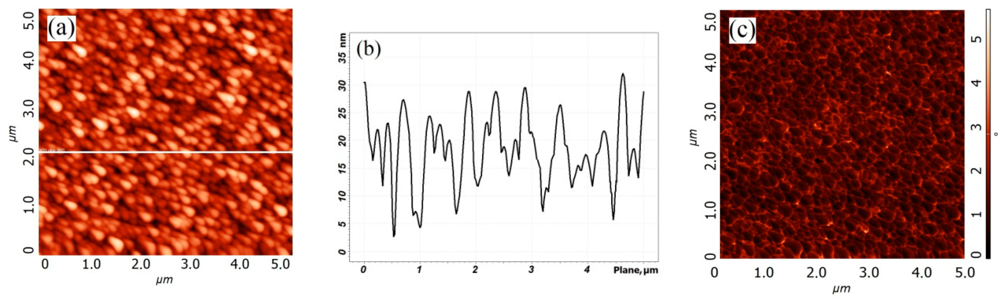
Figure 1 shows the experimental investigations of oxide vanadium film morphology grown at a substrate temperature of 650 °C. It was shown that the oxide vanadium film had a granular morphology (
Figure 1c) with 232.6 ± 76.1 nm grain diameter (
Figure 1c).
Analysis of the obtained experimental results showed that an increase in the substrate temperature (t
s) from 25 to 650 °C leads to an increase in the surface roughness from 4.3 ± 1.4 nm to 25.2 ± 4.4 nm (
Figure 2a). The nonlinear dependence can be associated with the difference in the phase and stoichiometric composition of the nanocrystalline vanadium oxide films at different substrate temperatures. Furthermore, analysis of the obtained experimental results showed that an increase in the annealing temperature (t
a) from 300 to 500 °C leads to an increase in the resistivity of vanadium oxide films from (2.03 ± 0.05) × 10
−2 up to (0.20 ± 0.11) × 10
2 Ω·cm (
Figure 2b). The sharp increase in the resistivity at t
a above 400 °C can be explained by the presence of a V
2O
5 phase and an abrupt change in the phase and stoichiometric composition of the nanocrystalline vanadium oxide film as the annealing temperature approaches the V
2O
5 melting temperature (670 °C).
Analysis of the obtained experimental results of studying the effect of resistive switching showed that CVC has nonlinear bipolar behavior when presumably the electric potential gradient is the dominant parameter of the effect of resistive switching [
13]. Resistive switching from HRS to LRS was observed at 1.37 ± 0.21 V (U
SET) and from LRS to HRS at −1.11 ± 0.37 V (U
RES) (
Figure 3a). In addition, analysis of the experimental results for the endurance test showed that R
HRS was (123.42 ± 21.77) × 10
3 Ω, R
LRS was (5.12 ± 1.36) × 10
2 Ω (
Figure 3b). R
HRS/R
LRS ratio was around 253.
Dispersion of resistances RHRS and RLRS can be explained by the uneven redistribution of the oxygen vacancy concentration profile in the volume of the nanocrystalline film of vanadium oxide when resistive switching occurs.
4. Conclusions
In summary, we studied some of the modes of synthesis of films of nanocrystalline vanadium oxide for the manufacture of ReRAM elements for neuromorphic systems. The regularities of the influence of pulsed laser deposition modes on the morphology and electrophysical properties of vanadium oxide films were experimentally established considering the technological parameters of the substrate temperature and the temperature of postgrowth annealing. It is shown that the change in substrate temperature from 25 to 650 °C, temperature of annealing in the range of 300 to 500 °C makes it possible to obtain nanocrystalline films of vanadium oxide film surface roughness in the range of 4.3 ± 1.4 to 25.2 ± 5.4 nm, with resistivity from (2.03 ± 0.05) × 10−2 up to (0.20 ± 0.11) × 102 Ω·cm. Resistive switching showed that USET = 1.37 ± 0.21 V, URES = −1.11 ± 0.37 V, RHRS = (123.42 ± 21.77) × 103 Ω, RLRS was (5.12 ± 1.36) × 102 Ω, and the RHRS/RLRS ratio was around 253. The results obtained can be used in the development of technological processes for the formation of nanocrystalline films of vanadium oxides for resistive memory elements in neuromorphic systems.
Author Contributions
Conceptualization and validation, O.A.A. and V.A.S.; methodology, V.A.S., R.V.T.; investigation, R.V.T., V.I.A. and A.A.A.; writing—original draft preparation, R.V.T. and V.A.S.; data curation and formal analysis, Z.E.V.; visualization R.V.T. and Z.E.V.; vanadium oxide film growth Z.E.V.; supervision, V.A.S.; project administration, writing—review and editing, O.A.A. All authors contributed to the writing of the manuscript, which was coordinated by O.A.A. and V.A.S. All authors have read and agreed to the published version of the manuscript.
Funding
The reported study was funded by Russian Foundation for Basic Research according to the research projects No. 19-29-03041_mk and No. 19-38-60052, and by grant of the President of the Russian Federation No. MK-6252.2021.4.
Institutional Review Board Statement
Not applicable.
Informed Consent Statement
Not applicable.
Data Availability Statement
Not applicable.
Acknowledgments
The results were obtained using the equipment of the Research and Education Center “Nanotechnology” at the Southern Federal University.
Conflicts of Interest
The authors declare no conflict of interest.
References
- Etienne-Cummings, R.; Van der Spiegel, J.; Mueller, P. Neuromorphic and digital hybrid systems. Neuromorphic Syst. Eng. Silicon Neurobiol. 1998, 1, 153–168. [Google Scholar]
- Smith, L.S. Neuromorphic systems: Past, present and future. Brain Inspired Cogn. Syst. 2008, 1, 167–182. [Google Scholar]
- Xia, Q.; Robinett, W.; Cumbie, M.W.; Banerjee, N.; Cardinali, T.J.; Yang, J.J.; Snider, G.S. Memristor—CMOS hybrid integrated circuits for reconfigurable logic. Nano Lett. 2009, 9, 3640–3645. [Google Scholar] [CrossRef] [PubMed]
- Indiveri, G.; Linares-Barranco, B.; Hamilton, T.J.; Van Schaik, A.; Etienne-Cummings, R.; Delbruck, T.; Schemmel, J. Neuromorphic silicon neuron circuits. Front. Neurosci. 2011, 5, 73. [Google Scholar] [CrossRef] [PubMed]
- Tominov, R.V.; Vakulov, Z.E.; Avilov, V.I.; Khakhulin, D.A.; Fedotov, A.A.; Zamburg, E.G.; Ageev, O.A. Synthesis and Memristor Effect of a Forming-Free ZnO Nanocrystalline Films. Nanomaterials 2020, 10, 1007. [Google Scholar] [CrossRef] [PubMed]
- Rozenberg, M.J.; Inoue, I.H.; Sanchez, M.J. Nonvolatile memory with multilevel switching: A basic model. Phys. Rev. Lett. 2004, 92, 178302. [Google Scholar] [CrossRef] [PubMed]
- Avilov, V.; Polupanov, N.; Tominov, R.; Solodovnik, M.; Konoplev, B.; Smirnov, V.; Ageev, O. Resistive Switching of GaAs Oxide Nanostructures. Materials 2020, 13, 3451. [Google Scholar] [CrossRef] [PubMed]
- Mikolajick, T.; Dehm, C.; Hartner, W.; Kasko, I.; Kastner, M.J.; Nagel, N.; Mazure, C. FeRAM technology for high density applications. Microelectron. Reliab. 2001, 41, 947–950. [Google Scholar] [CrossRef]
- Tehrani, S.; Slaughter, J.M.; Chen, E.; Durlam, M.; Shi, J.; DeHerren, M. Progress and outlook for MRAM technology. IEEE Trans. Magn. 1999, 35, 2814–2819. [Google Scholar] [CrossRef]
- Ageev, O.; Konoplev, B. Nanotechnology in Microelectronics, 1st ed.; Nauka Publisher: Moscow, Russia, 2019; p. 511. [Google Scholar]
- Smirnov, V. Nanolithography by local anodic oxidation of thin titanium film. In Piezoelectrics and Nanomaterials: Fundamentals, Developments and Applications, 1st ed.; Parinov, I., Ed.; Nova Science Publisher: Hauppauge, NY, USA, 2015; Volume 1, pp. 85–103. [Google Scholar]
- Khakhulin, D.A.; Vakulov, Z.E.; Smirnov, V.A.; Tominov, R.V.; Yoon, J.G.; Ageev, O.A. Resistive switching in ZnO/ZnO: In nanocomposite. J. Phys. Conf. Ser. 2017, 917, 092008. [Google Scholar] [CrossRef]
- Yang, J.J.; Strukov, D.B.; Stewart, D.R. Memristive devices for computing. Nat. Nanotechnol. 2013, 8, 13. [Google Scholar] [CrossRef] [PubMed]
| Publisher’s Note: MDPI stays neutral with regard to jurisdictional claims in published maps and institutional affiliations. |
© 2020 by the authors. Licensee MDPI, Basel, Switzerland. This article is an open access article distributed under the terms and conditions of the Creative Commons Attribution (CC BY) license (https://creativecommons.org/licenses/by/4.0/).


 ,
, 


