1. Introduction
Noble TMD (nTMD) 2D materials are displaying many fascinating properties including a widely tunable bandgap, moderate carrier mobility, anisotropy and high air stability [
1,
2,
3].
The nTMDs, and particularly the platinum diselenide PtSe
2, show diverse chemical and physical properties which are intensively studied especially in a 2D form [
4]. Their complex electronic structure with a notable indirect band gap can be tuned by several factors, such as varying the number of layers [
5], strain [
6] or induced defects [
7]. In monolayer form, PtSe
2 is semiconducting with a band gap in the range 1.2–1.8 eV [
2]. It turns into a semimetal by increasing the number of layers. Moreover, the charge–carrier mobility of PtSe
2 (values of 3000 cm
2/V·s [
4]) is among the highest in TMDCs and is comparable to black phosphorus (1000 cm
2/V·s [
8]) which makes it a promising candidate for high performance gas-sensing and photovoltaics, high-speed electronics and optoelectronics. PtSe
2 films grown by the thermally assisted conversion of platinum at a back-end-of-the-line complementary metal–oxide-semiconductor (CMOS) compatible temperatures show excellent promise for future applications [
9].
Another notable advantage of PtSe
2 is the environmental stability and appropriate synthesis requirements which are compatible with the conventional industrial technologies. The established synthesis approaches such as Thermally Assisted Conversion (TAC) [
4] and other methods such as Chemical Vapor Deposition [
10] and Molecular Beam Epitaxy [
11] show fine options for PtSe
2 nanostructure controllability and engineering for applications in opto-electronics, catalysis and sensors [
12,
13,
14].
The present study systematizes the initial technological steps of TAC synthesis of PtSe2 and the corresponding quality verification via structural and chemical characterization by XRD, Raman spectroscopy and XPS.
2. Materials Preparation and Methods
PtSe
2 films were synthesized by a twostep TAC procedure [
4]. The first (i) preparation stage facilitated a pre-deposition of Pt film using in a custom-built magnetron sputtering system with 3″ diameter Pt target (99.99% purity) by an RF (radio-frequency) magnetron sputtering process. The sputtering gas was argon of 99.999% purity. The applied power was set to 300 W and the deposition pressure was 6 × 10
−1 torr. The substrate holder was rotating during the sputtering run. The thickness of the deposited Pt films was controlled by the sputtering time. Pt thin films of varying thicknesses were deposited onto SiO
2/Si and the fused quartz substrate.
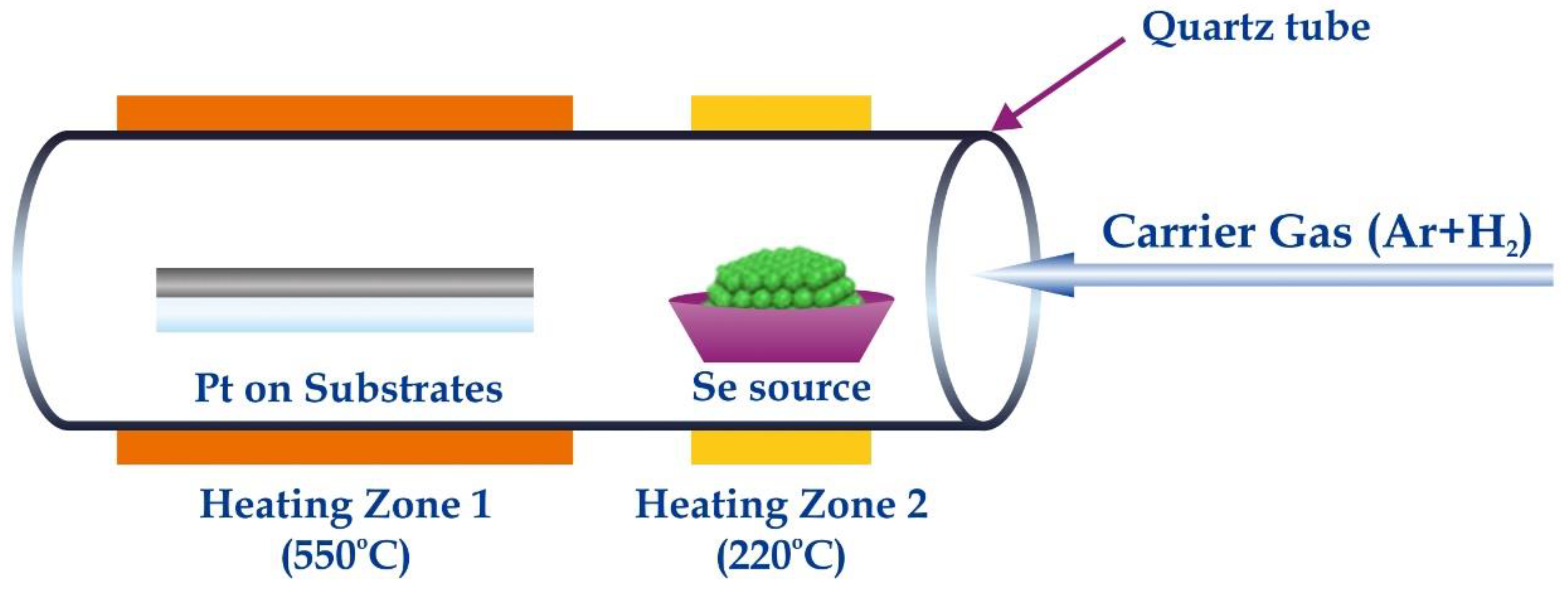
The second (ii) synthesis stage—a direct selenization of the pre-deposited films in a Chemical Vapor Deposition (CVD) reactor based on a dual zone tube furnace. The Se vapor (precursor powder) source and the Pt films on Si/SiO
2 are inserted as follows: in a low temperature zone (~220 °C) and in the growth high temperature zone (~550 °C), respectively. The process is mediated via a carrier/reactive gas mixture flow of 95% Ar/5% H
2 for 2 h with consequent formation of another necessary gaseous precursor—H
2Se to enable the PtSe
2 growth. A schematic of the CVD reactor is shown in
Figure 1.
The focus of the study is the synthesis details, structural and chemical characterizations of PtSe2 layers obtained from a 30 s Pt predisposition time. The X-ray diffraction patterns were collected using a Bruker D8 Advance diffractometer with Cu Kα radiation and a LynxEye detector within the range of 5.3° to 80° 2θ, with a constant step of 0.02°. The XPS analysis was performed using a Kratos AXIS Supra spectrometer with a non-monochromatic Al X-ray source under vacuum (<10−8 Pa) at a 90 take-off angle. The acquired photoelectron spectra were additionally processed using background signal subtraction and fitting procedures routines of the XPSPEAK41 software package. Raman spectroscopy measurements were carried out on an 80 cm Dilor XY-800, with a triple monochromator allowing for multi-channel liquid nitrogen cooled CCD (charge-coupled device) detection or single-channel PM detection. The experiments were performed at room temperature using 514.5 nm excitation line of a CW Ar+ laser.
3. Results and Discussion
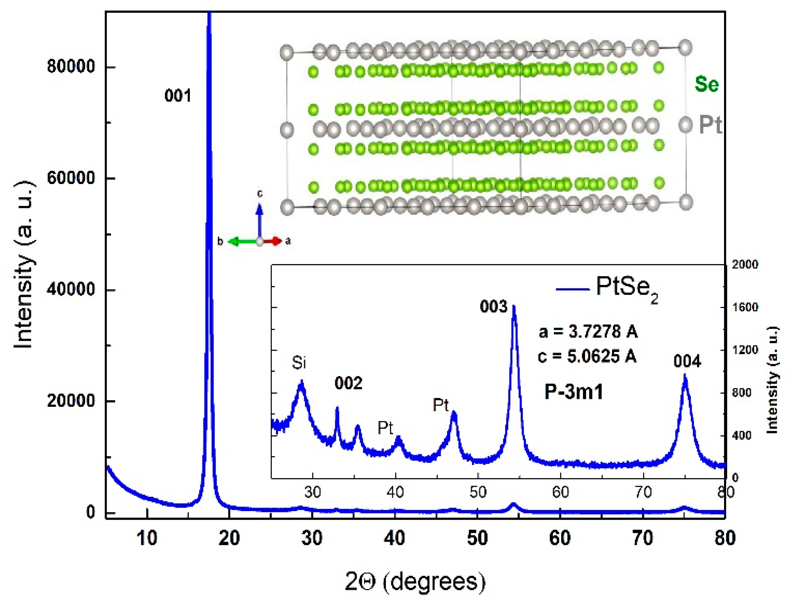
The physical nature of 2D materials, such as TMDs and particularly PtSe
2, is determined by the layered crystal structure (
Figure 2) with van der Waals stacking and strong anisotropy of the properties. The XRD pattern identify the PtSe
2 film crystal lattice with unit cell parameters determined to be a = 3.728 Å and c = 5.06 Å with hexagonal P3m1 (164) space group. The main (001) characteristic peak is detected approximately at 17.6° degrees 2θ. In the inset section an enlarged diffractogram sector (in the range 20–80°) is presented, showing the other peaks with diminished intensity as a consequence of the layered structure and dominant (001) orientation—implying a high crystalline quality and c-axis growth of the film plane. The peaks are assigned to (002), (003) and (004) crystallographic orientation and negligible traces (<1%) of Pt and the substrate SiO
2/Si (111) are also identified.
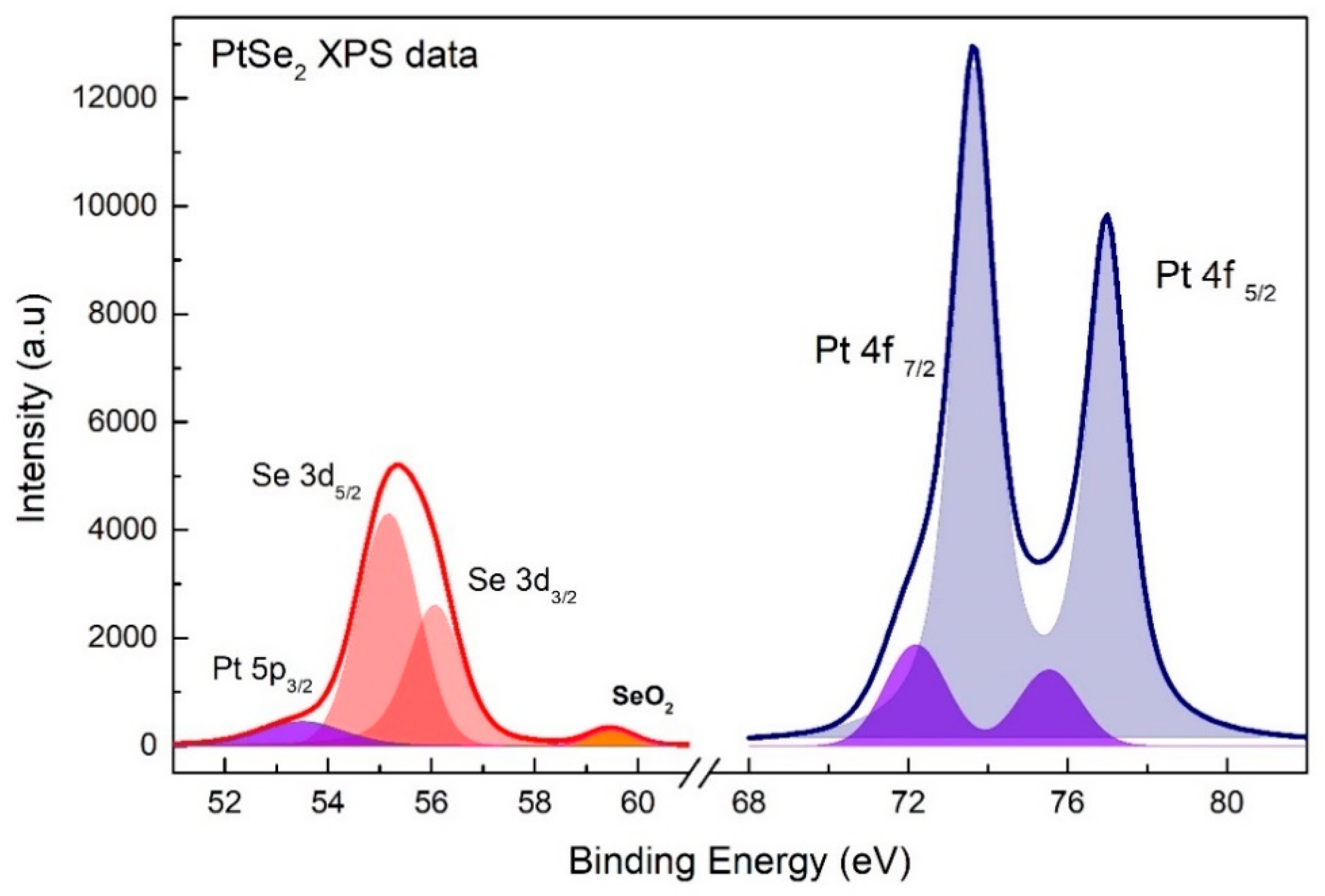
The chemical composition and binding energies of the PtSe
2 film were verified also by XPS. The spectrum (
Figure 3) shows the presence of both Pt and Se and the analysis data indicate that the PtSe
2 phase is successfully formed. The Se 3d peak is deconvoluted into two contributions: the main from PtSe
2 appears at around 55 eV (the spin-orbital splitting between Se 3d
5/2 and Se 3d
3/2 is 0.86 eV) and the minor with a binding energy around 59.5 eV typical for Se oxide. There are also traces for metallic state Pt in this range.
The Pt 4f is deconvoluted into two contributions; the one at ~72.3 eV is attributed to PtOx/hydroxide while the second one at ~73.6 eV was attributed to PtSe2. The spin-orbital splitting at 3.35 eV was used for the fitting procedure.
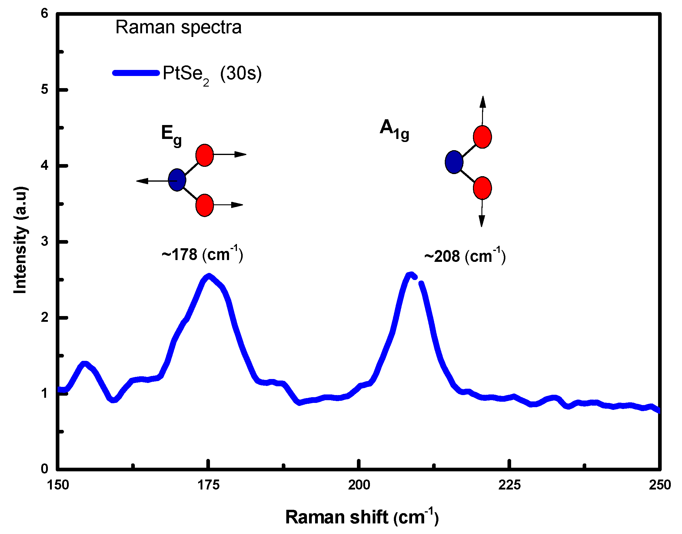
Raman spectroscopy is a powerful and nondestructive characterization technique which is widely used for 2D materials. The Raman spectra of TMDs are generally characterized by two main peaks corresponding to the in-plane and out-of-plane motions of atoms. The two Raman-active modes in the spectra of PtSe
2 are labeled as A
1g and E
g [
16]
A schematic of the vibrational modes in PtSe
2 is shown in
Figure 4, with arrows drawn as guides to show the origin of each mode on the phonon dispersion curve. These include the E
g mode, describing the in-plane vibration of selenium atoms in opposite directions within a single layer, and the A
1g mode describing the out-of-plane vibration of selenium atoms. The characteristic Raman active Eg (178 cm
−1) and A1g (208 cm
−1) mode of TAC deposited PtSe
2 confirm the composition and quality of the obtained samples.
4. Conclusions
The layered 2D material PtSe2 was successfully synthesized by a thermal assisted conversion process. The structural and chemical characterizations of the obtained PtSe2 confirm the composition and crystalline quality. The obtained results allow further directions for improvement of the preparation procedure (in particular the deposition periods) to facilitate the nanostructure synthesis approach towards the 2D PtSe2 applications.
Author Contributions
This article was coordinated by V.M.; all authors giving input to the written text. In particular, V.M., D.D. and K.B.; wrote most of the Introduction and Materials and Method, K.B.; interpreted XRD analyses, I.A.; performed and interpreted XPS analyses, D.D., H.D., and V.M.; synthesized the PtSe2 samples. Raman measurements and interpretation of the data were done by D.D.; with contribution from K.B. I.D.; contributed to visualization and data acquisition. All authors have read and agreed to the published version of the manuscript.
Funding
This work is supported by the Bulgarian Ministry of Education and Science under the National Research Programme “Young scientists and postdoctoral students” approved by DCM# 577/17.08.2018 and by Bulgarian Science Fund under the project КП-06-ДКOCT/1.
Conflicts of Interest
The authors declare no conflict of interest.
References
- Wang, Z.; Li, Q.; Besenbacher, F.; Dong, M. Facile Synthesis of Single Crystal PtSe2 Nanosheets for Nanoscale Electronics. Adv. Mater. 2016, 28, 10224–10229. [Google Scholar] [CrossRef] [PubMed]
- Zhao, Y.; Qiao, J.; Yu, Z.; Yu, P.; Xu, K.; Lau, S.P.; Zhou, W.; Liu, Z.; Wang, X.; Ji, W.; et al. High-Electron-Mobility and Air-STable 2D Layered PtSe2 FETs. Adv. Mater. 2017, 29, 1604230. [Google Scholar] [CrossRef] [PubMed]
- Pi, L.; Li, L.; Liu, K.; Zhang, Q.; Li, H.; Zhai, T. Recent Progress on 2D Noble-Transition-Metal Dichalcogenides. Adv. Funct. Mater. 2019, 29, 1904932. [Google Scholar] [CrossRef]
- Wang, Y.; Li, L.; Yao, W.; Song, S.; Sun, J.T.; Pan, J.; Ren, X.; Li, C.; Okunishi, E.; Wang, Y.-Q.; et al. Monolayer PtSe2, a New Semiconducting Transition-Metal-Dichalcogenide, Epitaxially Grown by Direct Selenization of Pt. Nano Lett. 2015, 15, 4013–4018. [Google Scholar] [CrossRef] [PubMed]
- Villaos, R.A.B.; Crisostomo, C.P.; Huang, Z.-Q.; Huang, S.-M.; Padama, A.A.B.; Albao, M.A.; Lin, H.; Chuang, F.-C. Thickness dependent electronic properties of Pt dichalcogenides. Npj 2D Mater. Appl. 2019, 3, 2. [Google Scholar] [CrossRef]
- Li, P.; Li, L.; Zeng, X.C. Tuning the electronic properties of monolayer and bilayer PtSe2 via strain engineering. J. Mater. Chem. C 2016, 4, 3106–3112. [Google Scholar] [CrossRef]
- Absor, M.A.U.; Santoso, I.; Harsojo; Abraha, K. ; Ishii, F.; Saito, M. Defect-induced large spin-orbit splitting in monolayer PtSe2. Phys. Rev. B 2017, 96, 115128. [Google Scholar] [CrossRef]
- Li, L.; Yu, Y.; Ye, G.J.; Ge, Q.; Ou, X.; Wu, H.; Feng, D.; Chen, X.H.; Zhang, Y. Black phosphorus field-effect transistors. Nat. Nanotechnol. 2014, 9, 372–377. [Google Scholar] [CrossRef] [PubMed]
- Wagner, S.; Yim, C.; McEvoy, N.; Kataria, S.; Yokaribas, V.; Kuc, A.; Pindl, S.; Fritzen, C.-P.; Heine, T.; Duesberg, G.S.; et al. Highly Sensitive Electromechanical Piezoresistive Pressure Sensors Based on Large-Area Layered PtSe2 Films. Nano Lett. 2018, 18, 3738–3745. [Google Scholar] [CrossRef] [PubMed]
- Yim, C.; Lee, K.; McEvoy, N.; O’Brien, M.; Riazimehr, S.; Berner, N.C.; Cullen, C.P.; Kotakoski, J.; Meyer, J.C.; Lemme, M.C.; et al. High-Performance Hybrid Electronic Devices from Layered PtSe2 Films Grown at Low Temperature. ACS Nano 2016, 10, 9550–9558. [Google Scholar] [CrossRef] [PubMed]
- Yan, M.; Wang, E.; Zhou, X.; Zhang, G.; Zhang, H.; Zhang, K.; Yao, W.; Lu, N.; Yang, S.; Wu, S.; et al. High quality atomically thin PtSe2 films grown by molecular beam epitaxy. 2D Mater. 2017, 4, 045015. [Google Scholar] [CrossRef]
- Al Mutairi, A.; Yin, D.; Yoon, Y. PtSe2 Field-Effect Transistors: New Opportunities for Electronic Devices. IEEE Electron. Device Lett. 2018, 39, 151–154. [Google Scholar] [CrossRef]
- Sajjad, M.; Montes, E.; Singh, N.; Schwingenschlögl, U. Superior Gas Sensing Properties of Monolayer PtSe2. Adv. Mater. Interfaces 2017, 4, 1600911. [Google Scholar] [CrossRef]
- Yim, C.; McEvoy, N.; Riazimehr, S.; Schneider, D.S.; Gity, F.; Monaghan, S.; Hurley, P.K.; Lemme, M.C.; Duesberg, G.S. Wide Spectral Photoresponse of Layered Platinum Diselenide-Based Photodiodes. Nano Lett. 2018, 18, 1794–1800. [Google Scholar] [CrossRef] [PubMed]
- Momma, K.; Izumi, F. VESTA 3 for three-dimensional visualization of crystal, volumetric and morphology data. J. Appl. Crystallogr. 2011, 44, 1272–1276. [Google Scholar] [CrossRef]
- O’Brien, M.; McEvoy, N.; Motta, C.; Zheng, J.-Y.; Berner, N.C.; Kotakoski, J.; Elibol, K.; Pennycook, T.J.; Meyer, J.C.; Yim, C.; et al. Raman characterization of platinum diselenide thin films. 2D Mater. 2016, 3, 021004. [Google Scholar] [CrossRef]
| Publisher’s Note: MDPI stays neutral with regard to jurisdictional claims in published maps and institutional affiliations. |
© 2020 by the authors. Licensee MDPI, Basel, Switzerland. This article is an open access article distributed under the terms and conditions of the Creative Commons Attribution (CC BY) license (https://creativecommons.org/licenses/by/4.0/).


