Proceeding Paper

Carbon-Based Perovskite Solar Cell †

1
Centre for Hybrid and Organic Solar Energy (CHOSE), Department of Electronic Engineering, University of Rome “Tor Vergata”, Via del Politecnico 1, 00133 Roma, Italy
2
Istituto di Struttura della Materia, Consiglio Nazionale delle Ricerche (ISM-CNR), Via del Fosso del Cavaliere 100, 00133 Roma, Italy
*
Author to whom correspondence should be addressed.
Presented at the 4th International Online Conference on Nanomaterials, 5–19 May 2023; Available online: https://iocn2023.sciforum.net/.
Mater. Proc. 2023, 14(1), 29; https://doi.org/10.3390/IOCN2023-14539
Published: 5 May 2023
(This article belongs to the Proceedings of The 4th International Online Conference on Nanomaterials)

Abstract

:
In a short period, Perovskite solar cell (PSC) technology gained high efficiency and broad attention because of its key enabling physical and morphological features. One of the main obstacles to the PSC industrialization and commercialization deals with the demonstration of stable devices by adopting low-cost and reliable materials and fabrication methods. In the n-i-p structure, the organic hole-transporting layer and the metal counter-electrodes are the main causes of instability and high cost. Here, we substituted these two elements with a low-temperature and low-cost carbon-based counter electrode.

1. Introduction

The constant and unceasing progress of technology in different areas requires renewable and green energy sources [1]. The photovoltaic (PV) sector has a fundamental role to cover the energy demand. To date, the PV market has been based mainly on the “first-generation” technology, i.e., monocrystalline and polycrystalline silicon, because of its high conversion efficiency of solar radiation into electricity. Despite that, the expensive manufacturing processes of silicon and its decreasing availability in nature have accelerated the exploitation of “second-generation” thin-film technologies based on materials such as cadmium telluride (CdTe) and amorphous silicon (a-Si) [2]. Moreover, the “third-generation” PV aims to maintain high efficiency by reducing production costs thanks to hybrid-organic materials on rigid and flexible substrates [3,4,5,6]. Natural dyes such as anthocyanins [7], polymers [8] and fullerenes [9] are just a few examples of molecules used for this purpose. The main issue concerning these new technologies is stability, since the organic molecules used are very sensitive to the operating conditions, such as temperature, prolonged exposure to UV light and humidity. The toxicity of the materials used and the synthesis/purification costs are issues to be addressed.
In the recent years, Perovskite (PVSK) has been widely used as photo-generator [10,11,12]. Its optical and electronic properties have allowed continuous development, reaching record efficiencies (close to 26%) in a few years [13]. PVSK is a chemical compound with an ABX3 formula, where A and B are cations with different atomic radii, and X represents an anion. Currently, regarding PVSKs, we refer to all crystalline solids with the same structure as CaTiO3 (bipyramidal crystalline cell with square base). Recently, perovskite-based materials—organometallic compounds of halogens—have gathered particular interest in the PV field thanks to their easy processability by solution together with efficiency comparable to the best inorganic materials used in optoelectronics such as gallium arsenide (GaAs) and Si.
Typically, a PVSK solar cell (PSC) is a layered structure, where each layer performs a well-defined function affecting the performance and the stability of the device. The PVSK is sandwiched between one electron transport layer (ETL) and a hole transport layer (HTL). The ETL and HTL are both connected to an external circuit by gold or silver contacts. In case of n-i-p architecture, ETL is generally composed by c-TiO2 (compact TiO2) and mp-TiO2 (mesoporous TiO2) or SnO2 and guarantees good conduction, low charge recombination and high transparency. The most widespread HTL is the 2,2′,7,7′-Tetrakis(N,Ndi-p-methoxyphenylamine)-9,9′- spirobifluorene. Spiro-MeOTAD ensures good energy levels of the band gap, a quick charge transfer and low recombination. However, there are still many related problems concerning the use of this material, e.g., operational environment sensitivity, high cost (about EUR 200/g), complex synthesis and low yield [14]. Moreover, spiro-OMeTAD is doped to increase the mobility of the holes with highly hygroscopic salts (lithiumbis(trifluoromethylsulfonyl)imide (Li-TFSI) or 4-tert-butylpyridine (t-BP)), leading to PSC degradation deterioration. Regarding the metal counter-electrode, gold diffuses into the structure of the device when exposed to continuous lighting, which causes damage. It is possible to replace both the organic HTL and the metal electrode with one low-temperature conductive carbon layer. Carbon materials are cheap when compared to HTMs (hole-transporting materials) and gold, resulting in a reduction of cells cost and an increase in stability. Carbon is a key material widely used in the PV field due to its abundance, low cost and appropriate energy level. Different kind of carbon materials [15,16,17], such as carbon nanotubes, carbon fiber and graphene, have been applied with success in many PV devices. In the PVSK field, the efficiencies are competitive with those measured in devices using spiro-OMeTAD as HTM [18,19,20,21,22,23]. Low-temperature carbon pastes, unlike the porous high-temperature inks [17,21], can be processed at temperatures below 130 °C, exhibiting features of high conductivity, low cost, good stability and high throughput processes.
In this paper, we demonstrate a simple process to fabricate HTL- and gold-free PSCs based on low-temperature carbon counter-electrodes by adopting solution-based processes for the full cell stack.

2. Materials and Methods

We adopted large area (1.01 cm2) of n-i-p cells as reported in Figure 1a.
We cleaned the FTO (fluorinated tin oxide) glasses (NSG, 8 Ω/sq.) in an ultrasonic system using subsequent solvents (soap/water, acetone, ethanol and isopropanol) for 5 min each. We deposited 30 nm-thick c-TiO2 as reported in [24] and 250 nm-thick mp-TiO2 paste (Great Cell Solar 18 nrt, diluted with ethanol 1:4 w/w) by the spin-coating, method followed by 30 min @ 500 °C sintering in an oven. The substrates were exposed to an UV lamp, and then we deposited the triple cation PVSK (Cs0.05(MA0.17FA0.83)0.95Pb(I0.83Br0.17)3 in DMF/DMSO, 1.42 M) (PbI2 from TCI Co., Ltd., Tokyo, Japan; CsI, FAI and MABr from Great Cell Solar, Queanbeyan, Australia) by the spin-coating method in a glovebox. The spin-coating parameters to deposit the precursor solution were as follows: first step: 1000 rpm, 5 s ramping, 10 s; second step: 5000 rpm, 2 s ramping, 30 s; chlorobenzene dropped 7 s before the end. Then, the PVSK was annealed 60 min @ 100 °C. In a recent publication, we demonstrated how to upscale the triple cation PVSK formulation to the module device [24]. Regarding the gold-based cells, a Spiro-OMeTAD (Borum, Hadsten, Denmark) HTM solution was prepared and deposited according to [14]. Following this, 85 nm-thick gold and 30 µm carbon (Dyenamo, Stockholm, Sweden) counter-electrodes were thermally evaporated and blade-coated, respectively. The carbon-based cells were annealed at 60 °C in vacuum and 120 °C in air for 15 min in the case of Spiro HTM and HTM-free, respectively. The JV curves and the stability measurements were reported by a Keithley source meter/LabVIEW under a class A sun simulator (Sun 2000, Abet, Milford, Connecticut, USA) at AM 1.5 1000 W/m2 calibrated by a Skye Instruments sensor Ltd (Llandrindod Wells, UK).

3. Results and Discussion

The JV curves are depicted in Figure 1b and Table 1.
In the case of PVSK/Spiro/carbon cells, all electrical parameters were lower with respect to the PVSK/carbon cells. Most likely, capacitive and recombination phenomena occurred at the Spiro/Carbon interface, with this inefficient setup affecting not only the fill factor, but also the current and Voc. A lower FF mainly affected the PCE, as shown by the comparison of PVSK/carbon with PVSK/HTL/Gold cells, due to the lower conductivity of the carbon electrode compared to the gold electrode. It is also important to underline how the hysteresis phenomena are practically absent in the case of carbon-based cells by comparing the hysteresis index (HI) in Table 1 [26]. In the case of PVSK/carbon cells, the short-circuit current density (Jsc) was about 19 mA/cm2, as reported in Figure 1b and Table 1. The best efficiencies were 13.4% and 10.2% for the PVSK/HTL/Gold and PVSK/Carbon devices, respectively (Figure 1b, Table 1). After 5 min in the light condition at maximum power, the device lost just 4% efficiency and remained stable at 9.8% (Figure 1c, Table 1).

4. Conclusions

The PV exploitation should avoid high-cost and high-CO2 footprint materials and fabrication processes. The adoption of low-temperature carbon PSC counter-electrodes makes it possible to avoid expensive organic HTM and metal counter-electrodes, such as gold and silver. These materials are also sources of degradation, leading to low stability in the presence of moisture, high temperature and light. Moreover, the carbon inks can be deposited by large-area printing techniques, such as screen-printing and blade-coating [27]. Since the carbon layer can be annealed at temperatures less than 120 °C, the impact from the LCA (life cycle assessment) point of view is low. Here, we demonstrated how the PSCs can work without any HTL or loss of efficiency. Further, studies on low-cost 2D PVSK strategies are ongoing to improve the electrical parameters of the cells. Moreover, the scaling up to module and stability assessment according to the ISOS standard is ongoing.

Author Contributions

Conceptualization, L.V.; methodology, L.V.; validation, L.V. and A.D.C.; formal analysis, L.V. and M.S.; investigation, M.S. and L.V.; resources, A.D.C.; data curation, L.V. and M.S.; writing—original draft preparation, L.V.; writing—review and editing, L.V.; visualization, L.V.; supervision, A.D.C. and L.V.; project administration, A.D.C. and L.V.; funding acquisition, A.D.C. and L.V. All authors have read and agreed to the published version of the manuscript.

Funding

This research was funded by the European Union’s Horizon 2020 programme, through an FET Proactive research and innovation action under grant agreement No. 101084124 (DIAMOND). The authors acknowledge the project UNIQUE, supported under the umbrella of SOLARERA. NET_cofund by ANR, PtJ, MUR (GA 775970), MINECOAEI, SWEA, within the European Union Framework Program for Research and Innovation Horizon 2020 (Cofund ERANET Action, No. 691664).

Institutional Review Board Statement

Not applicable.

Informed Consent Statement

Not applicable.

Data Availability Statement

Data supporting reported results are available in repository.

Conflicts of Interest

The authors declare no conflict of interest.

References

  1. Eftekharnejad, S.; Vittal, V.; Heydt, G.T.; Keel, B.; Loehr, J. Impact of increased penetration of photovoltaic generation on power systems. IEEE Trans. Power Syst. 2013, 28, 893–901. [Google Scholar] [CrossRef]
  2. Barkhouse, D.A.R.; Gunawan, O.; Gokmen, T.; Todorov, T.K.; Mitzi, D.B. Yield predictions for photovoltaic power plants:empirical validation, recent advances and remaining uncertainties. Prog. Photovolt. Res. Appl. 2015, 20, 6–11. [Google Scholar] [CrossRef]
  3. Mincuzzi, G.; Vesce, L.; Liberatore, M.; Reale, A.; Di Carlo, A.; Brown, T.M. Laser-sintered TiO2 films for dye solar cell fabrication: An electrical, morphological, and electron lifetime investigation. IEEE Trans. Electron Devices 2011, 58, 3179–3188. [Google Scholar] [CrossRef]
  4. Barichello, J.; Vesce, L.; Mariani, P.; Leonardi, E.; Braglia, R.; Di Carlo, A.; Canini, A.; Reale, A. Stable semi-transparent dye-sensitized solar modules and panels for greenhouse application. Energies 2021, 14, 6393. [Google Scholar] [CrossRef]
  5. Zardetto, V.; De Angelis, G.; Vesce, L.; Caratto, V.; Mazzuca, C.; Gasiorowski, J.; Reale, A.; Di Carlo, A.; Brown, T.M. Formulations and processing of nanocrystalline TiO2 films for the different requirements of plastic, metal and glass dye solar cell applications. Nanotechnology 2013, 24, 255401. [Google Scholar] [CrossRef]
  6. Dominici, L.; Vesce, L.; Colonna, D.; Michelotti, F.; Brown, T.M.; Reale, A.; Di Carlo, A. Angular and prism coupling refractive enhancement in dye solar cells. Appl. Phys. Lett. 2010, 96, 42. [Google Scholar] [CrossRef]
  7. Yuvapragasam, A.; Muthukumarasamy, N.; Agilan, S.; Velauthapillai, D.; Senthil, T.S.; Sundaram, S. Natural dye sensitized TiO2 nanorods assembly of broccoli shape based solar cells. J. Photochem. Photobiol. B Biol. 2015, 148, 223–231. [Google Scholar] [CrossRef]
  8. Etxebarria, I.; Ajuria, J.; Pacios, R. Solution-processable polymeric solar cells: A review on materials, strategies and cell architectures to overcome 10%. Org. Electron. 2015, 19, 34–60. [Google Scholar] [CrossRef]
  9. Zhang, G.; Ning, H.; Chen, H.; Jiang, Q.; Jiang, J.; Han, P.; Dang, L.; Xu, M.; Shao, M.; He, F.; et al. Naphthalenothiophene imide-based polymer exhibiting over 17% efficiency. Joule 2021, 5, 931–944. [Google Scholar] [CrossRef]
  10. Kojima, A.; Teshima, K.; Shirai, Y.; Miyasaka, T. Organometal halide perovskites as visible-light sensitizers for photovoltaic cells. J. Am. Chem. Soc. 2009, 131, 6050–6051. [Google Scholar] [CrossRef]
  11. Snaith, H.J. Present status and future prospects of perovskite photovoltaics. Nat. Mater. 2018, 17, 372–376. [Google Scholar] [CrossRef] [PubMed]
  12. Feng, S.-P.; Cheng, Y.; Yip, H.-L.; Zhong, Y.; Fong, P.W.K.; Li, G.; Ng, A.; Chen, C.; Castriotta, L.A.; Matteocci, F.; et al. Roadmap on Commercialization of Metal Halide Perovskite Photovoltaics. J. Phys. Mater. 2023, 6, 032501. [Google Scholar] [CrossRef]
  13. Green, M.A.; Dunlop, E.D.; Hohl-Ebinger, J.; Yoshita, M.; Kopidakis, N.; Bothe, K.; Hinken, D.; Rauer, M.; Hao, X. Solar cell efficiency tables (Version 60). Prog. Photovolt. Res. Appl. 2022, 30, 687–701. [Google Scholar] [CrossRef]
  14. Vesce, L.; Stefanelli, M.; Di Carlo, A. Efficient and stable perovskite large area cells by low-cost fluorene-xantene-based hole transporting layer. Energies 2021, 14, 6081. [Google Scholar] [CrossRef]
  15. Calabrò, E.; Matteocci, F.; Paci, B.; Cinà, L.; Vesce, L.; Barichello, J.; Generosi, A.; Reale, A.; Di Carlo, A. Easy Strategy to Enhance Thermal Stability of Planar PSCs by Perovskite Defect Passivation and Low-Temperature Carbon-Based Electrode. ACS Appl. Mater. Interfaces 2020, 12, 32536–32547. [Google Scholar] [CrossRef]
  16. Barichello, J.; Vesce, L.; Matteocci, F.; Lamanna, E.; Di Carlo, A. The effect of water in Carbon-Perovskite Solar Cells with optimized alumina spacer. Sol. Energy Mater. Sol. Cells 2019, 197, 76–83. [Google Scholar] [CrossRef]
  17. Vesce, L.; Riccitelli, R.; Mincuzzi, G.; Orabona, A.; Soscia, G.; Brown, T.M.; Di Carlo, A.; Reale, A. Fabrication of spacer and catalytic layers in monolithic dye-sensitized solar cells. IEEE J. Photovolt. 2013, 3, 1004–1011. [Google Scholar] [CrossRef]
  18. Stefanelli, M.; Vesce, L.; Di Carlo, A. Upscaling of Carbon-Based Perovskite Solar Module. Nanomaterials 2023, 13, 313. [Google Scholar] [CrossRef]
  19. Liu, Z.; Shi, T.; Tang, Z.; Sun, B.; Liao, G. Using a low-temperature carbon electrode for preparing hole-conductor-free perovskite heterojunction solar cells under high relative humidity. Nanoscale 2016, 8, 7017–7023. [Google Scholar] [CrossRef]
  20. Chu, Q.Q.; Ding, B.; Qiu, Q.; Liu, Y.; Li, C.X.; Li, C.J.; Yang, G.J.; Fang, B. Cost effective perovskite solar cells with a high efficiency and open-circuit voltage based on a perovskite-friendly carbon electrode. J. Mater. Chem. A 2018, 6, 8271–8279. [Google Scholar] [CrossRef]
  21. Bogachuk, D.; Zouhair, S.; Wojciechowski, K.; Yang, B.; Babu, V.; Wagner, L.; Xu, B.; Lim, J.; Mastroianni, S.; Pettersson, H.; et al. Low-Temperature Carbon-based Electrodes in Perovskite Solar Cells. Energy Environ. Sci. 2020, 13, 3880–3916. [Google Scholar] [CrossRef]
  22. Jiang, P.; Jones, T.W.; Duffy, N.W.; Anderson, K.F.; Bennett, R.; Grigore, M.; Marvig, P.; Xiong, Y.; Liu, T.; Sheng, Y.; et al. Fully printable perovskite solar cells with highly-conductive, low-temperature, perovskite-compatible carbon electrode. Carbon 2018, 129, 830–836. [Google Scholar] [CrossRef]
  23. Lin, S.; Yang, B.; Qiu, X.; Yan, J.; Shi, J.; Yuan, Y.; Tan, W.; Liu, X.; Huang, H.; Gao, Y.; et al. Efficient and stable planar hole-transport-material-free perovskite solar cells using low temperature processed SnO2 as electron transport material. Org. Electron. 2018, 53, 235–241. [Google Scholar] [CrossRef]
  24. Vesce, L.; Stefanelli, M.; Herterich, J.P.; Castriotta, L.A.; Kohlstädt, M.; Würfel, U.; Di Carlo, A. Ambient Air Blade-Coating Fabrication of Stable Triple-Cation Perovskite Solar Modules by Green Solvent Quenching. Sol. RRL 2021, 5, 2100073. [Google Scholar] [CrossRef]
  25. Chen, B.; Yang, M.; Priya, S.; Zhu, K. Origin of J-V Hysteresis in Perovskite Solar Cells. J. Phys. Chem. Lett. 2016, 7, 905–917. [Google Scholar] [CrossRef]
  26. Ren, J.; Kan, Z. Chapter 1: Origin of Hysteresis in Perovskite Solar Cells; AIP Publishing LLC: Melville, NY, USA, 2020; Volume 1, ISBN 9780735422414. [Google Scholar]
  27. Vesce, L.; Guidobaldi, A.; Mariani, P.; Di Carlo, A.; Parisi, M.L.; Maranghi, S.; Basosi, R. Scaling-up of Dye Sensitized Solar Modules. In World Scientific Reference of Hybrid Materials; World Scientific: Singapore, 2019; Volume 2, pp. 423–485. [Google Scholar]
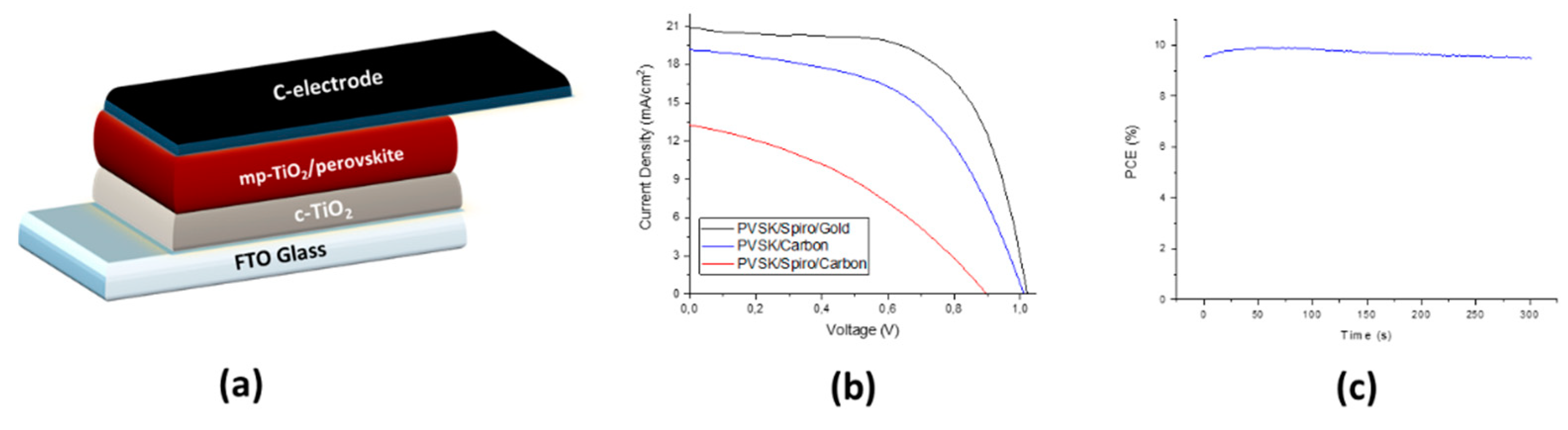
Figure 1. (a) PSC layers; (b) JV curves measurements; (c) Stability by MPP tracking.
Materproc 14 00029 g001
Table 1. Electrical parameters of the fabricated devices. HI is the Hysteresis Index [25].
Cell StackVoc (V)Jsc (mA/cm2)FF (%)PCE (%)HI
TiO2/PVSK/Spiro/Carbon0.9012.67394.401.20
TiO2/PVSK/Carbon1.01195310.201.05
TiO2/PVSK/Spiro/Gold1.0220.306513.401.25
Disclaimer/Publisher’s Note: The statements, opinions and data contained in all publications are solely those of the individual author(s) and contributor(s) and not of MDPI and/or the editor(s). MDPI and/or the editor(s) disclaim responsibility for any injury to people or property resulting from any ideas, methods, instructions or products referred to in the content.

