Proceeding Paper

A Novel Dielectric Modulated Misaligned Double-Gate Junctionless MOSFET as a Label-Free Biosensor †

by
Saurabh Kumar
* and
Rajeev Kumar Chauhan
Department of Electronics & Communication Engineering, Madan Mohan Malaviya University of Technology, Gorakhpur 273010, India
*
Author to whom correspondence should be addressed.
Presented at the 3rd International Electronic Conference on Biosensors, 8–21 May 2023; Available online: https://iecb2023.sciforum.net.
Eng. Proc. 2023, 35(1), 8; https://doi.org/10.3390/IECB2023-14578
Published: 8 May 2023
(This article belongs to the Proceedings of The 3rd International Electronic Conference on Biosensors)

Abstract

:
This research paper presents a misaligned double-gate junctionless Metal-Oxide-Semiconductor Field-Effect Transistor for label-free detection of biomolecules. The proposed biosensor combines the advantages of being junctionless, as well as possessing double and misaligned gate MOSFETs, which results in improved sensitivity and selectivity for biological recognition. The results show that the proposed biosensor can effectively detect biomolecules and has the potential for use in various applications. Biosensors have become an important tool in various fields, such as healthcare, environmental monitoring, and food safety due to their ability to detect biomolecules. MOSFETs have been widely used as biosensors due to their less complex structure and ease of use. However, traditional MOSFETs have limitations in terms of sensing performance, and there is a need for improved designs that overcome these limitations. The results of this study show that the proposed biosensor can effectively detect various biomolecules, such as protein and DNA. The proposed biosensor design has the potential to revolutionize the field of biosensors. Its combination of improved sensitivity and selectivity makes it a valuable tool for various applications. In conclusion, this research paper presents a dielectric modulated novel misaligned double-gate junctionless MOSFET-based biosensor, promising improved sensing performance in various applications. The proposed design provides a valuable contribution to the field of biosensors and has the potential to revolutionize the way biomolecules are detected.

1. Introduction

The need for a highly sensitive, reliable, and cost-effective biosensors has been a long-standing challenge in the field of medical diagnostics and biological research. In recent years, extensive research has been carried out to develop biosensors based on various technologies, such as surface plasmon resonance, quartz crystal microbalance, and field-effect transistors (FETs) [1,2,3]. Among these, FET-based biosensors have shown tremendous potential due to their high sensitivity, label-free detection, real-time monitoring capabilities, and potential for miniaturization [4,5,6,7,8]. FET-based biosensors rely on the modulation of the electric field at the interface between the gate and the sensing layer to detect biomolecules [9].
Several research works have been carried out to enhance the sensitivity and selectivity of FET-based biosensors using various strategies, such as surface modification, gate functionalization, and gate dielectric modulation. Despite the progress in FET-based biosensors, their sensitivity and selectivity remain a major concern for real-world applications. Therefore, there is a need to explore new device structures and sensing principles to address these challenges. Furthermore, researchers have explored various gate dielectric materials to improve the sensitivity of FET-based biosensors. For instance, the use of high-k dielectrics, such as hafnium oxide (HfO2) and aluminium oxide (Al2O3), has been reported to increase the capacitance of the gate and, hence, enhance the electric field modulation [10,11]. However, these strategies have limitations in terms of cost-effectiveness, reproducibility, and scalability.
The proposed structure overcomes the above discussed limitations and offers several advantages, such as high sensitivity, selectivity, and real-time monitoring capabilities. This novel biosensor has the potential to revolutionize the field of medical diagnostics, drug discovery, and environmental monitoring. The proposed biosensor uses Cr2O3 as a gate dielectric to improve the sensitivity of the device [3]. In this research paper, we propose a novel dielectric modulated misaligned double-gate junction less MOSFET (DM-MDG JL-MOSFET) structure as a label-free biosensor. The misaligned double-gate structure enables improved control over the electric field, which enhances the sensitivity of the device. One such strategy is the use of chromic oxide (Cr2O3) as a gate dielectric. Cr2O3 is an interesting material for FET-based biosensors because of its high dielectric constant, stability, and biocompatibility. The use of Cr2O3 as a gate dielectric has been reported to enhance the capacitance of the gate and improve the sensitivity of FET-based biosensors [3,12]. However, to the best of our knowledge, the proposed DM-MDG JL-MOSFET biosensor structure has not been reported in the literature.

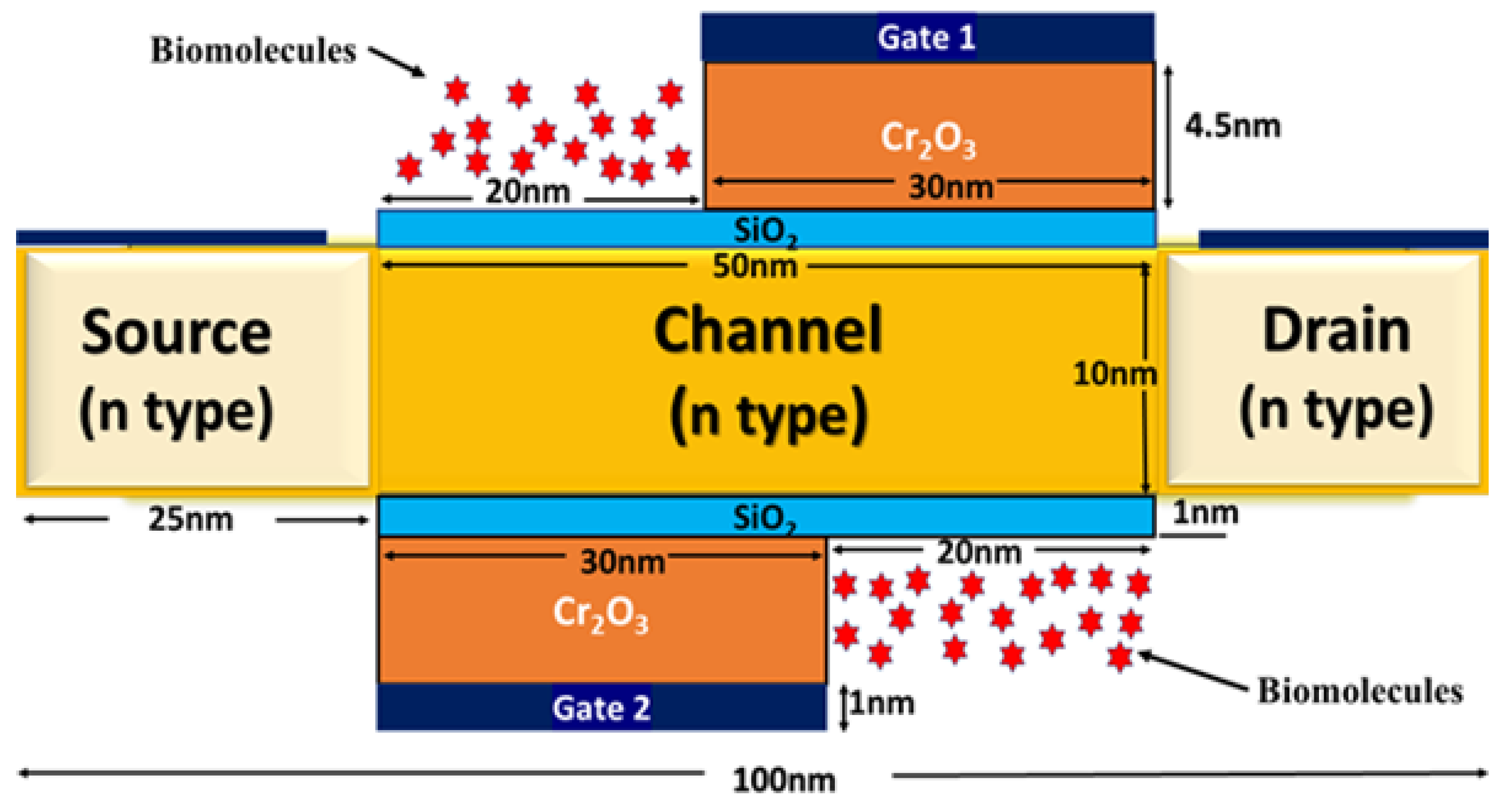
2. Device Description

A DM-MDG JL-MOSFET biosensor is shown in Figure 1. The device has a channel length of 50 nm, a cavity length of 20 nm, and a channel thickness of 10 nm. It consists of a silicon substrate on which a layer of oxide is deposited, comprising a 1 nm layer of SiO2 and a 4.5 nm layer of Cr2O3. Drain-to-source voltage (VDS) is kept at 0.5 V, and gate-to-source voltage (VGS) is kept at 1.5 V while simulating the device. The other parameters used in the device are mentioned in the Table 1. When considering protein biomolecules in the cavity region, the dielectric constant (K) is increased (K > 1), keeping charge (NBIO) at the Si–SiO2 layer at zero. Similarly, for examining the effect of DNA biomolecules, a non-zero charge is considered at the Si–SiO2 layer with the dielectric constant [3].
The misaligned double-gate structure is created by depositing a gate electrode on each side of the channel. The gates are misaligned, such that they do not completely overlap with each other, which helps to reduce the gate capacitance and improve the device performance. In this work, the Atlas device simulator is used for simulation and for obtaining results [13].

3. Findings and Discussion

The biomolecules are immobilized in the nanogap, or the cavity changes the electrical parameter of the proposed biosensor, as shown in Figure 2 and Figure 3. When the dielectric constant of the biomolecule’s changes (K > 1), it can have an impact on several electrical parameters of the DM-MDG JL-MOSFET biosensor. When biomolecules with different dielectric constants are immobilized in the cavity region, the gate capacitance can change. This change in capacitance modulates the conductance of the device and, thus, its electrical response [14]. Changes in the gate capacitance can alter the sensitivity of the DM-MDG JL-MOSFET biosensor. The sensitivity of the device is directly proportional to the change in conductance resulting from the biomolecular interaction. Therefore, a higher change in gate capacitance would result in a higher sensitivity [15]. The detection limit of the DM-MDG JL-MOSFET biosensor is also affected by the change in gate capacitance, resulting from the biomolecular interaction. A higher change in gate capacitance allows the device to detect lower concentrations of biomolecules. Overall, the electrical parameters of a DM-MDG JL-MOSFET biosensor can vary with changes in the dielectric constant of the biomolecules of interest. These variations are crucial for optimizing the performance of the biosensor in detecting specific biomolecules with high sensitivity and low detection limits [16].
Subthreshold swing is defined as the change in gate voltage required to change the drain current by one decade (tenfold) [17]. In a DM-MDG JL-MOSFET biosensor, the subthreshold swing can vary with changes in the gate capacitance and the charge carrier density in the channel region. When the gate capacitance changes due to the bio molecular interaction, the subthreshold swing can also change [17]. A lower subthreshold swing results in higher sensitivity and lower detection limit. Figure 2a depicts a change in threshold voltage and subthreshold swing due to change in dielectric constant of the neutral biomolecules. A higher dielectric constant of the biomolecules results in a higher gate capacitance and a higher ON current, which are depicted in Figure 2b. A change in ION/IOFF ratio is 30.61% with the change in dielectric constant K = 1 (air) to K = 12 (biomolecules). A higher transconductance results in a more sensitive biosensor, as it indicates that a small change in the gate voltage can produce a larger change in the drain current [18]. This higher sensitivity can be used to detect lower concentrations of biomolecules in biological or environmental samples. Figure 2c shows a change of 17.26% in transconductance with the change in dielectric constant from K = 1 (air) to K = 12 (biomolecules).
A single unhybridized strand of DNA has both dielectric constant and a charge, which, when hybridized, results in an increment on the dielectric constant of the unfilled nanogap. The relative dielectric constant of DNA is taken to be 8 [3]. Figure 3b depicts the impact of NBIO variation on the drain current. From Figure 3a,b, it has been observed that the impact of varying NBIO on drain current (ID) is relatively greater than the impact of varying K.

4. Conclusions

This work proposes a new type of biosensor that utilizes a misaligned double-gate junctionless MOSFET structure. The device is designed to detect changes in the electrical properties of the channel caused by the presence of biological molecules on the surface of the gate electrodes. The results of the study demonstrate the potential of the proposed device for use in label-free biosensing applications, with high sensitivity. The proposed biosensor has several advantages over traditional biosensors, including label-free detection, high sensitivity, and low power consumption. Moreover, the misaligned double-gate structure reduces the gate capacitance and improves the device performance. The results of the study demonstrate the potential of the proposed device for use in medical diagnosis, environmental monitoring, and other applications.

Author Contributions

Conceptualization, methodology, simulation, validation, analysis, investigation, resources, data curation, writing—original draft preparation, writing—review and editing, visualization, S.K. and R.K.C.; supervision, project administration, funding acquisition, R.K.C. All authors have read and agreed to the published version of the manuscript.

Funding

This research received no external funding.

Institutional Review Board Statement

Not applicable.

Informed Consent Statement

Not applicable.

Data Availability Statement

The data presented in this study are available within this article’s content.

Conflicts of Interest

The authors declare no conflict of interest.

References

  1. Han, H.-C.; Chang, Y.-R.; Hsu, W.-L.; Chen, C.-Y. Application of parylene-coated quartz crystal microbalance for on-line real-time detection of microbial populations. Biosens. Bioelectron. 2009, 24, 1543–1549. [Google Scholar] [CrossRef] [PubMed]
  2. Shrivastav, A.M.; Cvelbar, U.; Abdulhalim, I. A comprehensive review on plasmonic-based biosensors used in viral diagnostics. Commun. Biol. 2021, 4, 70. [Google Scholar] [CrossRef] [PubMed]
  3. Kumar, S.; Chauhan, R.K. Performance analysis of dielectric modulated underlap FD-SOI MOSFET for biomolecules detection. Appl. Phys. A 2022, 128, 1104. [Google Scholar] [CrossRef]
  4. Li, Z.; Xiao, M.; Jin, C.; Zhang, Z. Toward the Commercialization of Carbon Nanotube Field Effect Transistor Biosensors. Biosensors 2023, 13, 326. [Google Scholar] [CrossRef] [PubMed]
  5. Bulgakova, A.; Berdyugin, A.; Naumova, O.; Fomin, B.; Pyshnyi, D.; Chubarov, A.; Dmitrienko, E.; Lomzov, A. Solution pH Effect on Drain-Gate Characteristics of SOI FET Biosensor. Electronics 2023, 12, 777. [Google Scholar] [CrossRef]
  6. Manimekala, T.; Sivasubramanian, R.; Dharmalingam, G. Nanomaterial-Based Biosensors using Field-Effect Transistors: A Review. J. Electron. Mater. 2022, 51, 1950–1973. [Google Scholar] [CrossRef] [PubMed]
  7. Zhu, Z.; Garcia-Gancedo, L.; Flewitt, A.J.; Xie, H.; Moussy, F.; Milne, W.I. A Critical Review of Glucose Biosensors Based on Carbon Nanomaterials: Carbon Nanotubes and Graphene. Sensors 2012, 12, 5996–6022. [Google Scholar] [CrossRef] [PubMed]
  8. Elli, G.; Hamed, S.; Petrelli, M.; Ibba, P.; Ciocca, M.; Lugli, P.; Petti, L. Field-Effect Transistor-Based Biosensors for Environmental and Agricultural Monitoring. Sensors 2022, 22, 4178. [Google Scholar] [CrossRef] [PubMed]
  9. Kumar, S.; Chauhan, R.; Kumar, M. Sensitivity Enhancement of Dual Gate FET Based Biosensor Using Modulated Dielectric for COVID Detection. Silicon 2022, 14, 11453–11462. [Google Scholar] [CrossRef]
  10. He, G.; Sun, Z.; Li, G.; Zhang, L. Review and Perspective of Hf-based High-k Gate Dielectrics on Silicon. Crit. Rev. Solid State Mater. Sci. 2012, 37, 131–157. [Google Scholar] [CrossRef]
  11. Bencherif, H.; Yousfi, A.; Dehimi, L.; Pezzimenti, F.; Corte, F.G.D. Analysis of Al2O3high-k gate dielectric effect on the electrical characteristics of a 4H-SiC low-power MOSFET. In Proceedings of the 2019 1st International Conference on Sustainable Renewable Energy Systems and Applications (ICSRESA), Tebessa, Algeria, 4–5 December 2019; pp. 8–11. [Google Scholar] [CrossRef]
  12. Kwan, C.-P.; Chen, R.; Singisetti, U.; Bird, J.P. Electric-field dependent conduction mechanisms in crystalline chromia. Appl. Phys. Lett. 2015, 106, 112901. [Google Scholar] [CrossRef]
  13. SILVACO Int. ATLAS User’s Manual; SILVACO Int.: Santa Clara, CA, USA, 2014. [Google Scholar]
  14. Chowdhury, D.; De, B.P.; Appasani, B.; Singh, N.K.; Kar, R.; Mandal, D.; Bizon, N.; Thounthong, P. A Novel Dielectric Modulated Gate-Stack Double-Gate Metal-Oxide-Semiconductor Field-Effect Transistor-Based Sensor for Detecting Biomolecules. Sensors 2023, 23, 2953. [Google Scholar] [CrossRef] [PubMed]
  15. Rahman, E.; Shadman, A.; Khosru, Q.D. Effect of biomolecule position and fill in factor on sensitivity of a Dielectric Modulated Double Gate Junctionless MOSFET biosensor. Sens. Bio-Sens. Res. 2017, 13, 49–54. [Google Scholar] [CrossRef]
  16. Reddy, N.N.; Panda, D.K. Design and investigation of dielectric modulated triple metal gate-oxide-stack Z-shaped gate horizontal pocket TFET device as a label-free biosensor. J. Micromech. Microeng. 2022, 32, 085001. [Google Scholar] [CrossRef]
  17. Maduagwu, U.A.; Srivastava, V.M. Analytical Performance of the Threshold Voltage and Subthreshold Swing of CSDG MOSFET. J. Low Power Electron. Appl. 2019, 9, 10. [Google Scholar] [CrossRef]
  18. Chang, K.-M.; Chang, C.-T.; Chan, K.-M. Development of an Ion Sensitive Field Effect Transistor Based Urea Biosensor with Solid State Reference Systems. Sensors 2010, 10, 6115–6127. [Google Scholar] [CrossRef] [PubMed]
Figure 1. Device structure.
Engproc 35 00008 g001
Figure 2. Variation in (a) threshold voltage and subthreshold swing, (b) ON current and OFF current, (c) ON and OFF current ration and transconductance with immobilization of various biomolecules.
Engproc 35 00008 g002
Figure 3. Variation in drain current for (a) different dielectric constant (b) for different charge density.
Engproc 35 00008 g003
Table 1. Physical parameters of the proposed device.
Parameters of the Proposed DeviceValues
Upper and lower gate work function4.9 eV
Channel (doping concentration) 1   ×   10 17   c m 3
Source (doping concentration) 1   ×   10 20   c m 3
Drain (doping concentration) 5   ×   10 18   c m 3
Length of the source and drain region25 nm
Disclaimer/Publisher’s Note: The statements, opinions and data contained in all publications are solely those of the individual author(s) and contributor(s) and not of MDPI and/or the editor(s). MDPI and/or the editor(s) disclaim responsibility for any injury to people or property resulting from any ideas, methods, instructions or products referred to in the content.

