1. Introduction
VO
2 has many important applications because of its uniquely reversible phase transitioning properties [
1,
2,
3,
4]. There have been numerous studies reported on synthesizing high quality VO
2 on different substrates and their electrical and optical properties have been investigated in detail. While traditionally VO
2 is grown on sapphire, Si or quartz substrates, its synthesis on muscovite substrate has attracted special attention due to the optical transparency and flexibility of muscovite, which not only offers the possibility of modulating the optical properties of the transmitted light through phase transition but can enable the phase transition by application of mechanical strain. However, the typical transition temperature of 67 °C is not low enough to induce phase change by application of strain, in unheated substrates, which can enable a host of applications requiring high sensitivity associated with the phase change region. Therefore, reduction in the transition temperature of the VO
2 is very much desired, which will make the VO
2 thin film will be more sensitive to physical parameters such as temperature, strain or electric field even at room temperature without any need for heating, enabling it to be used as a thermal sensor with great sensitivity. This can be achieved by doping the vanadium with metallic dopants such as W, Ti and Cr, which can reduce the transition temperature of VO
2 thin films [
5,
6]. In our previous reports [
7,
8] we have demonstrated the synthesis and properties of VO
2 synthesized on various substrates, including piezoelectric and flexible ones. We also displayed the shifting of transition temperature due to mechanical strain on VO
2 on muscovite [
7] In the current work, we present the phase transitioning properties of VO
2 doped with Ti and compared the characteristics of doped and undoped VO
2. Furthermore, we displayed the change of resistance of VO
2 film due to mechanical strain.
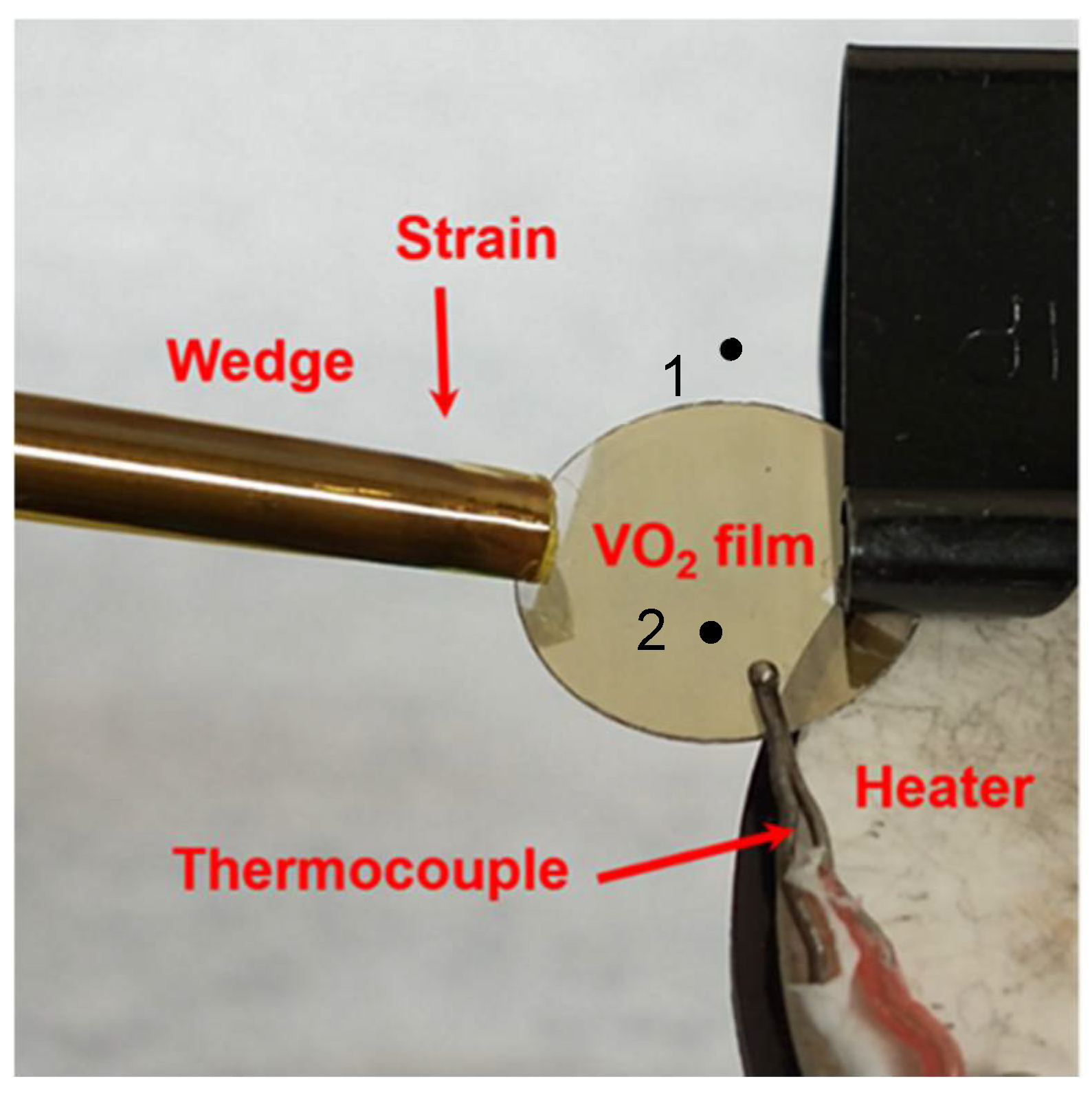
For measuring the surface resistance, the VO
2 thin film sample is connected to a data acquisition unit through contact points formed by conductive paste. The sample is placed at the very edge of the ceramic heater with a thermocouple on top of it to record the real-time temperature, operated from the data acquisition unit (
Figure 1). The temperature is varied through by the ceramic heater, which is recorded by the data acquisition unit, alongside the real-time variation of resistance. In order to apply the mechanical strain, a wedge was placed on top or bottom of the sample, to apply tensile or compressive strain, respectively. The amount of strain was controlled by the rotation of a knob of the micropositioner attached to the wedge. In order to observe the effect of strain on surface resistance, the temperature of the sample was maintained at room temperature, and for each amount of tensile and compressive strain, the resistance was recorded. A gradual reduction of resistance was observed due to increase of compressive strain, whereas the opposite behavior is observed for tensile strain. The same measurement procedure was repeated at transition temperature 50 °C and similar results were observed. Gauge factor has been calculated for all the three combinations of applied strain on the VO
2/Ti/muscovite, i.e., tensile strain at room temperature, compressive strain at room temperature and compressive strain at transition region of VO
2. As expected, maximum gauge factor was obtained at the transition region of VO
2 due to compressive strain.
3. Results and Discussion
The experimental setup in
Figure 1 was utilized to measure the electrical resistance variation. A two-point probe measurement setup was implemented to observe the effect of substrate heating on the electrical resistance of VO
2 following previously reported [
9,
10]. A ceramic heater is used to vary the temperature of the VO
2 film, assisted by a thermocouple for recording the temperature, and tungsten probes connected to a data acquisition unit for measuring the surface resistance. The results are plotted in
Figure 1.
As seen from
Figure 1a,b, the Ti-doped VO
2 shows a significant reduction in transition temperature from 70 °C to 35 °C. However, this is also associated with a reduction in the transition resistance ratio from 958 to 36. On the other hand, the transition temperature for the VO
2 synthesized on muscovite changed from 61 °C to 47 °C, while the transition resistance ratio reduced from 417 to 99.
The effect of strain on VO2 based sensing films deposited on the muscovite substrate was studied using a home-made experimental set up as shown in
Figure 2.
A thermocouple is also shown touching the VO
2 substrate to measure the film temperature. We studied both tensile and compressive strain by bending the edge of the film using a micropositioner extended arm. The arm is pressed downwards on the top of the sample to create tensile strain, and it can be pressed upwards from the bottom of the sample to produce compressive strain. The tensile strain causes the surface resistance to increase while compressive strain results in a decrease in surface resistance in agreement with previous reports [
8].
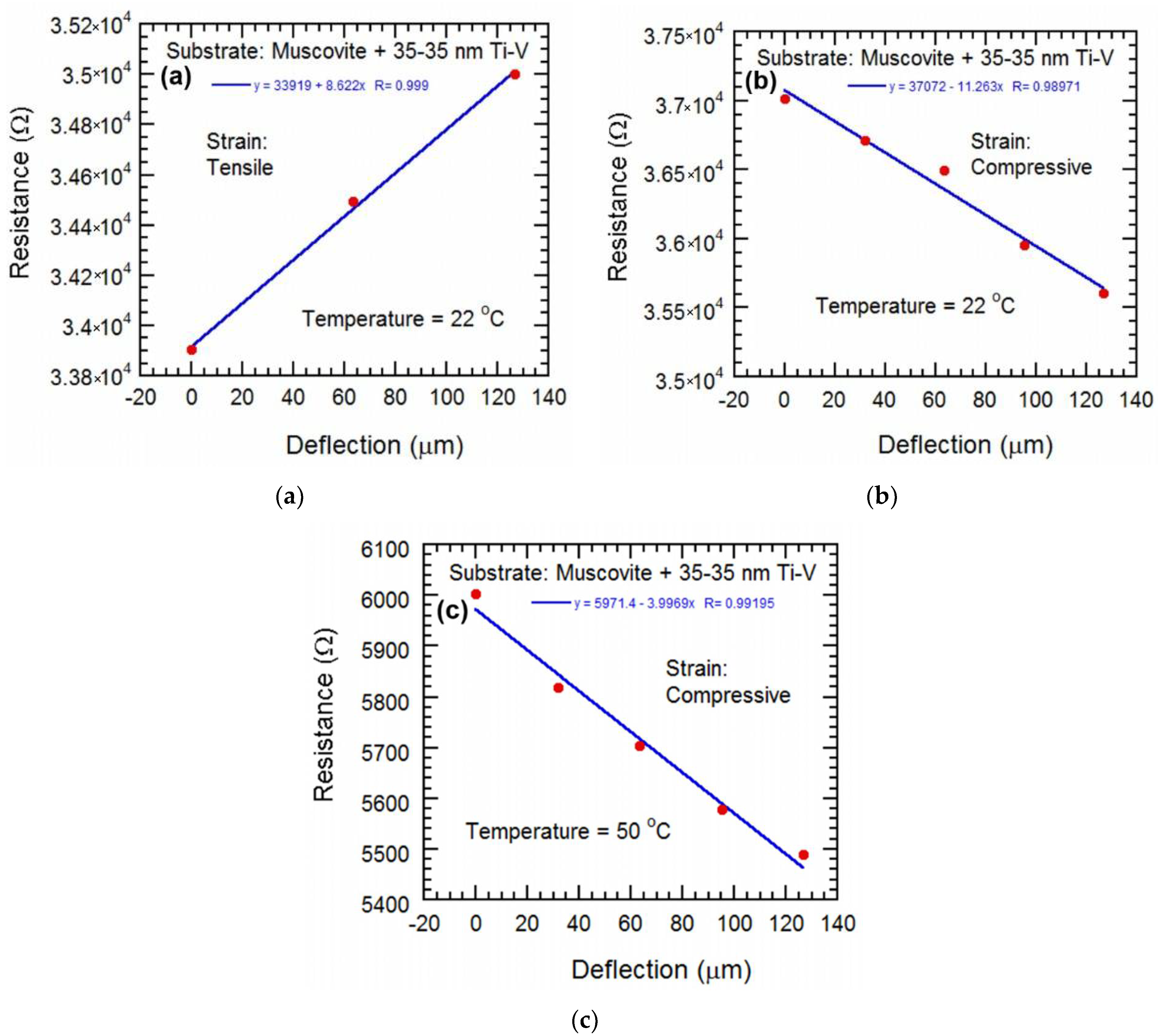
In
Figure 3, the variation of surface resistance is plotted with respect to variation of deflection due to applied strain. The change of resistance is recorded with change of tensile strain at room temperature, compressive strain at room temperature and compressive strain around transition temperature at phase transitioning region. For tensile strain the change in resistance per °C comes out to be 3.55%. The slope of resistance change is significantly more at the phase transition region compared to room temperature. At room temperature due to compressive strain, rate of change of resistance per °C is 5.95% and for around transition temperature, it is 9.09%.
The VO
2/Ti/muscovite thin film sample shown in
Figure 2 can be approximated as a square cantilever with thickness
t = 150 µm, and beam length
L = 11 mm (1.1 × 10
4 µm), one end attached and the other end as freely suspended. From
Figure 3a–c, we see that the maximum deflection of the free end of the cantilever
Ymax = 127 µm.
The length to thickness ratio of the approximated cantilever is 73:1, which is more than 10:1. Therefore, the average strain ε due to deflection of the free end of the cantilever can be calculated from the formula stated below [
11]:
Here, t is the cantilever beam thickness, L is the cantilever beam length, and Y is the cantilever deflection at the free end.
Plugging in the values of the parameters of the right-hand side of the Equation (1), we can calculate the strain as
ε = 2.36 × 10
−4. From
Figure 3a, the fractional resistance change (over the entire deflection range) can be calculated as Δ
R/
R = 0.032 for tensile strain at 22 °C. From the maximum deflection
Ymax = 127 µm, the gauge factor GF is calculated from the formula [
12]:
Plugging in the values of the right-hand side of the Equation (2), the calculated gauge factor = 136. Following the same procedure, the relative resistance change for 127 μm deflection in
Figure 3b comes out to be the Δ
R/
R = 0.038, which yields a GF value for the compressive strain at 22 °C as 161. Similarly, from the plot in
Figure 3c, we find Δ
R/
R = 0.086, and for the compressive strain of
ε = 2.36 × 10
−4, the GF turns out to be 364 at 50 °C.
Comparing the GF values in all three cases, we find that the gauge factor is maximum when the relative variation of resistance is maximum during compressive strain, which happens at the phase transition region (50 °C).
Comparing the GF values with those of common semiconductors, we find that these values are significantly higher than the best values reported for Si piezoresistors, which have the maximum gauge factor 95 [
12]. They are also comparable to the GF values reported for III-nitride based piezoresistors, although they are lower than that which is possible with the III-Nitride piezotransistor technology. For III-V based piezoresistive microcantilevers, the gauge factor reported previously for tensile strain was 75 [
13]. The GF of 136 determined for tensile strain in this work is higher than the GF calculated for tensile strain on III-V based piezoresistive microcantilevers [
13].
For III-V nitride-based pressure sensors with integrated transistors [
14], the maximum gauge factor reported be 260 for operation in the sub-threshold region, which is still less than the maximum gauge factor 364 found for our flexible VO
2/Ti/muscovite thin films at phase transition temperature. However, piezotransistors formed by GaN microcantilever with embedded AlGaN/GaN HFET provides gauge factor ~8700 for gate bias voltage −3 V, caused by a deflection of only 1 µm [
15], and 3200 due to gate bias voltage of −3.1 V [
16], which are still much superior compared to the values reported here for our macroscopic devices. Nonetheless, the presented VO
2 based sensing devices required no specialized and expensive layer structures such as the III-Nitrides or complicated fabrication methodology. Thus, they can be promising for applications requiring near room temperature strain sensing requiring high sensitivity.


