Passive Intermodulation at Contacts of Rough Conductors


Abstract
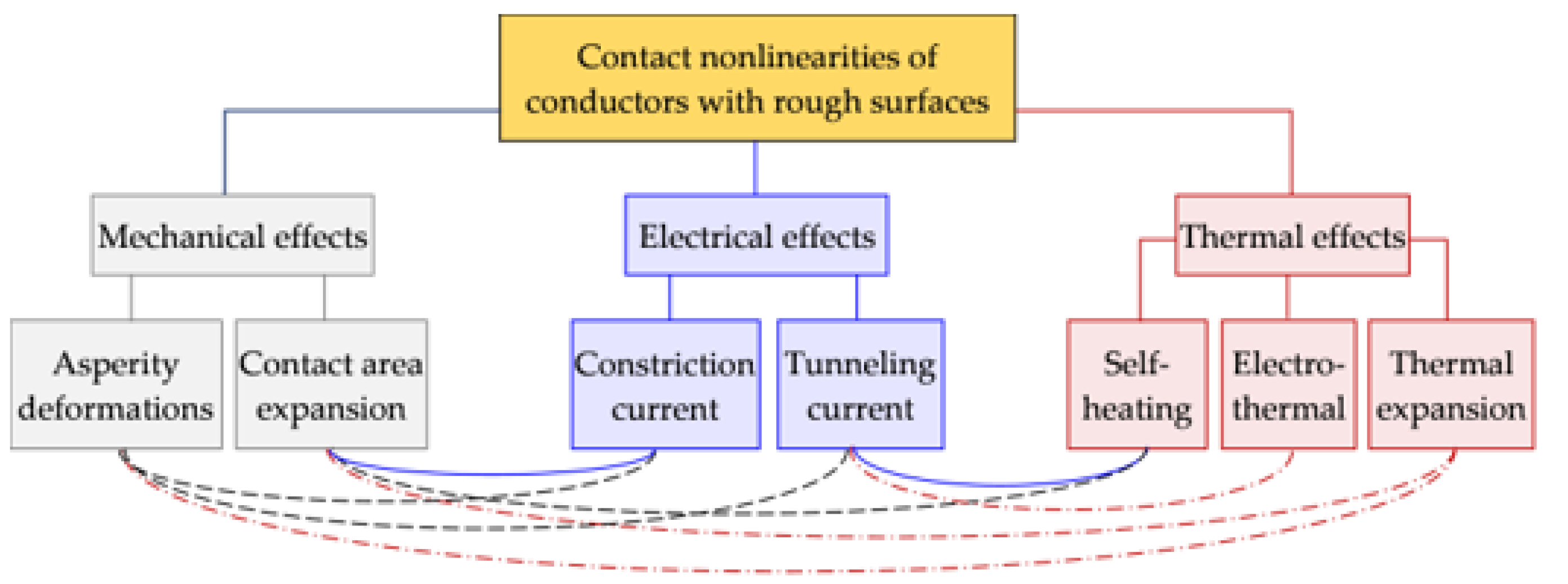
:1. Introduction
- -
- Charge tunnelling and diffusion at MIM junctions of conductor asperities;
- -
- Current constriction at asperities of rough contact surfaces;
- -
- Self-heating and thermal expansion of the contact surfaces and asperities;
- -
- Electro-thermal effect due to ohmic losses in conductors and contacts;
- -
- Asperity deformations of the conductors with rough surfaces and their contacts subjected to mechanical stresses, expansion and creep.
2. Electrical Nonlinearities of Conductor Joints
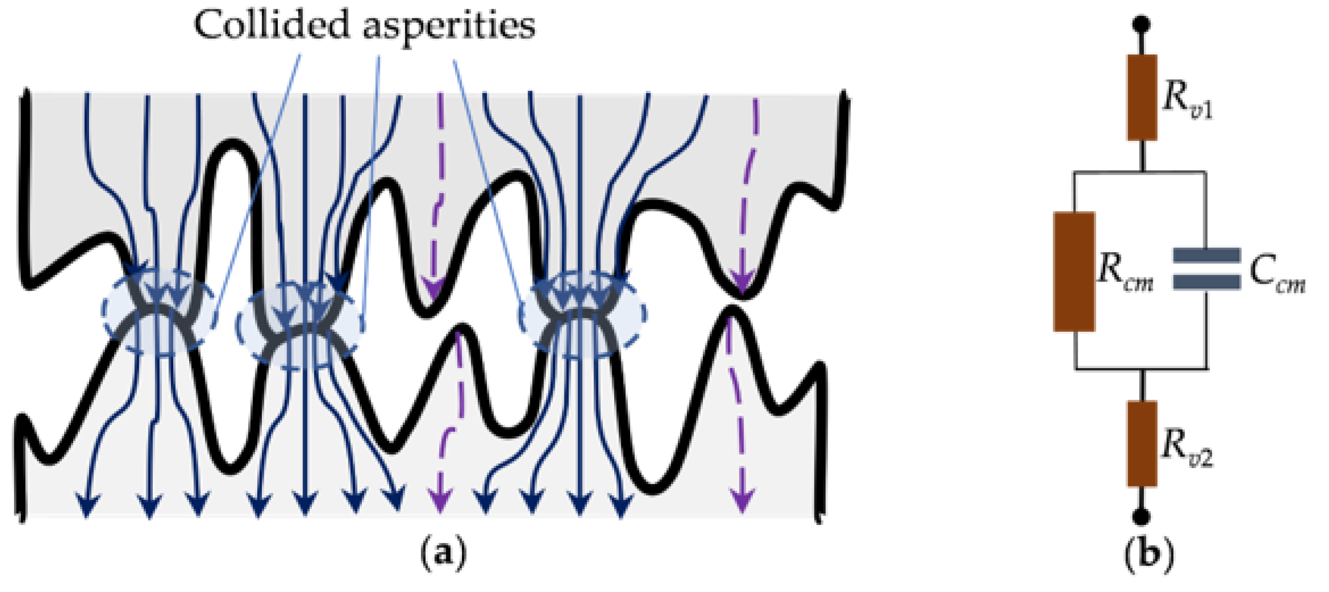
2.1. Contact and Constriction Resistances
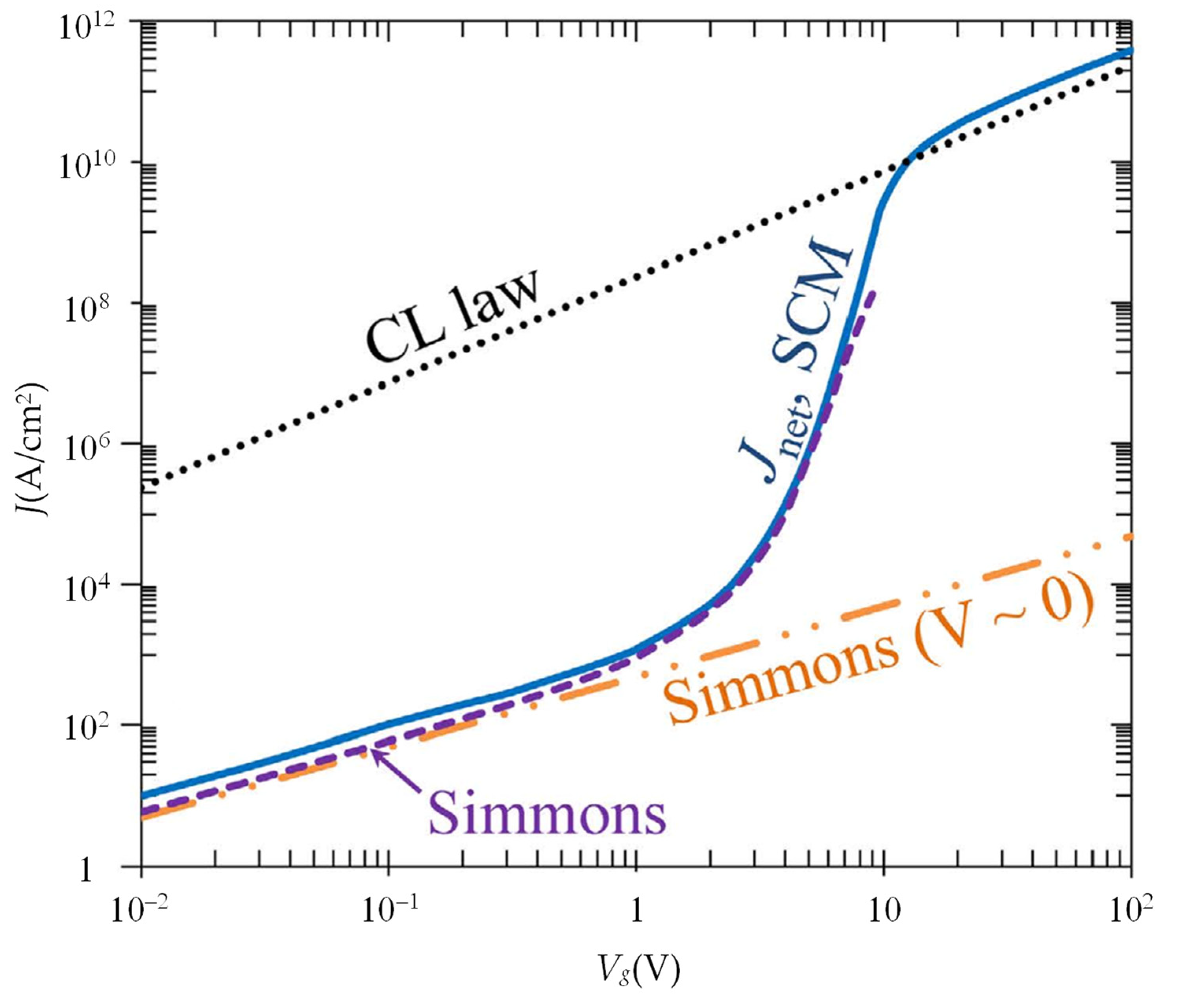
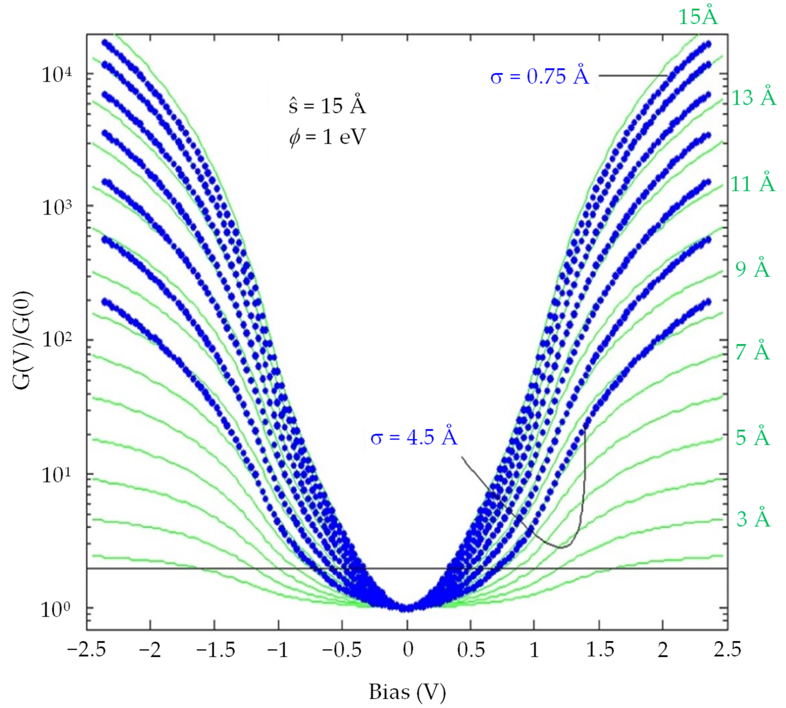
2.2. Nonlinearity of MIM Contacts
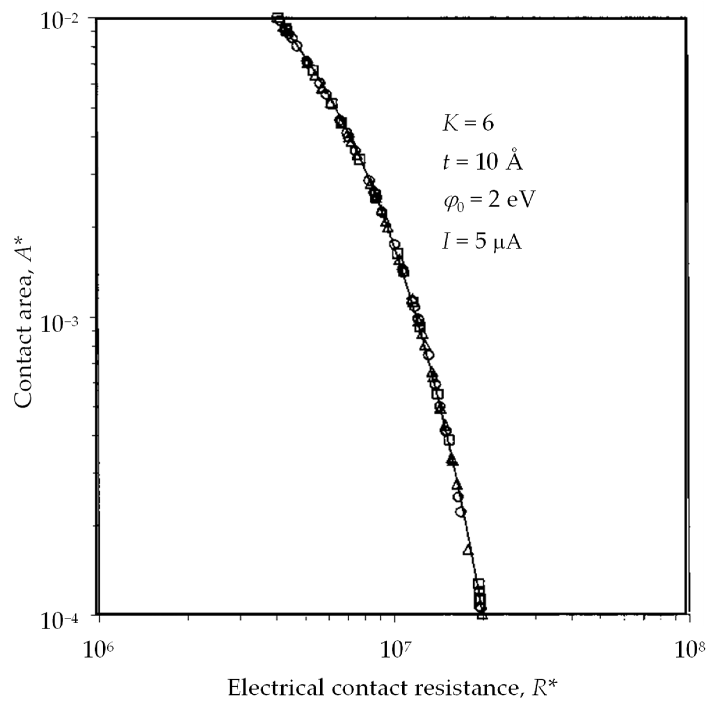
2.3. The Effect of Surface Roughness
2.4. Thermionic Emission
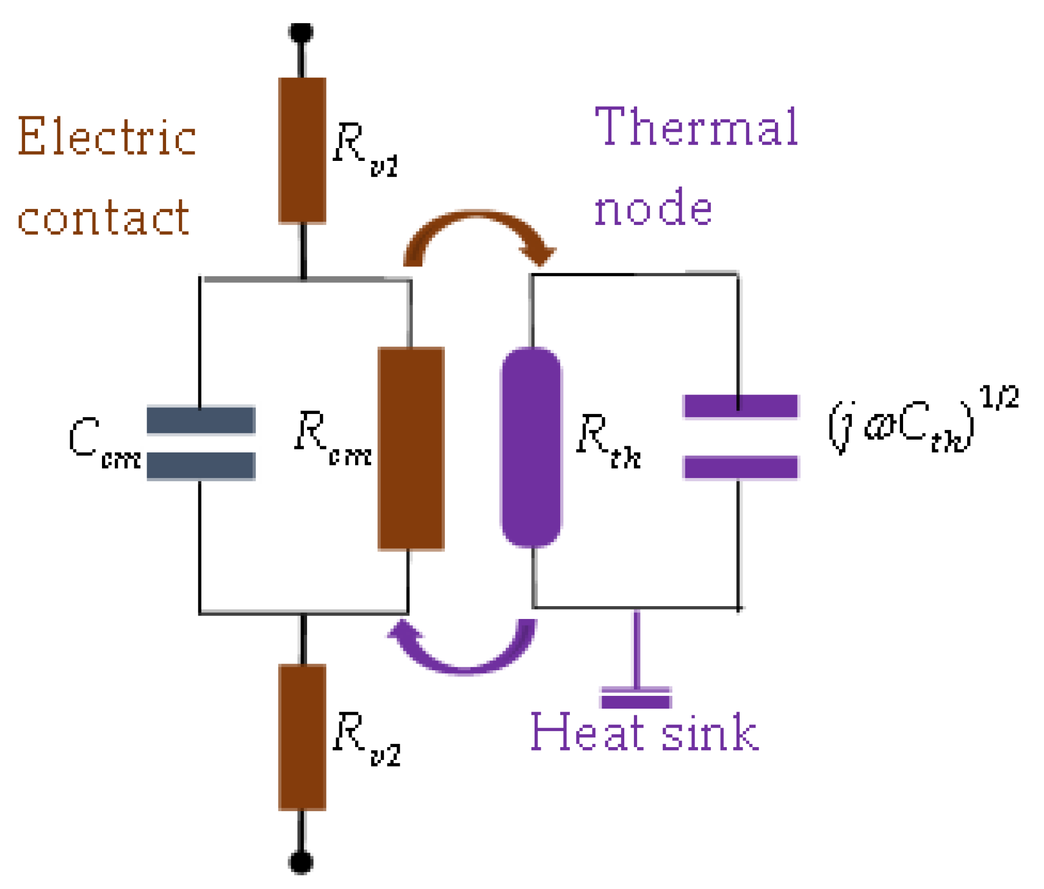
3. Thermal Nonlinearities at Contacts of Good Conductors
3.1. Self-Heating Effect and Nonlinearity of Contact Resistivity
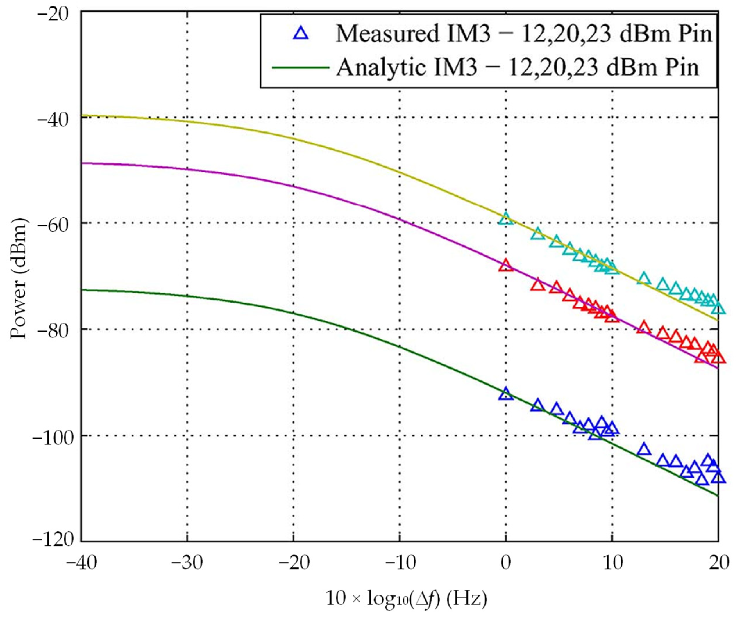
3.2. Electro-Thermal Effect in Contact Joints and PIM Generation
3.3. Thermal Expansion of the Contact Area
4. Mechanical Nonlinearities at Conductor Contacts
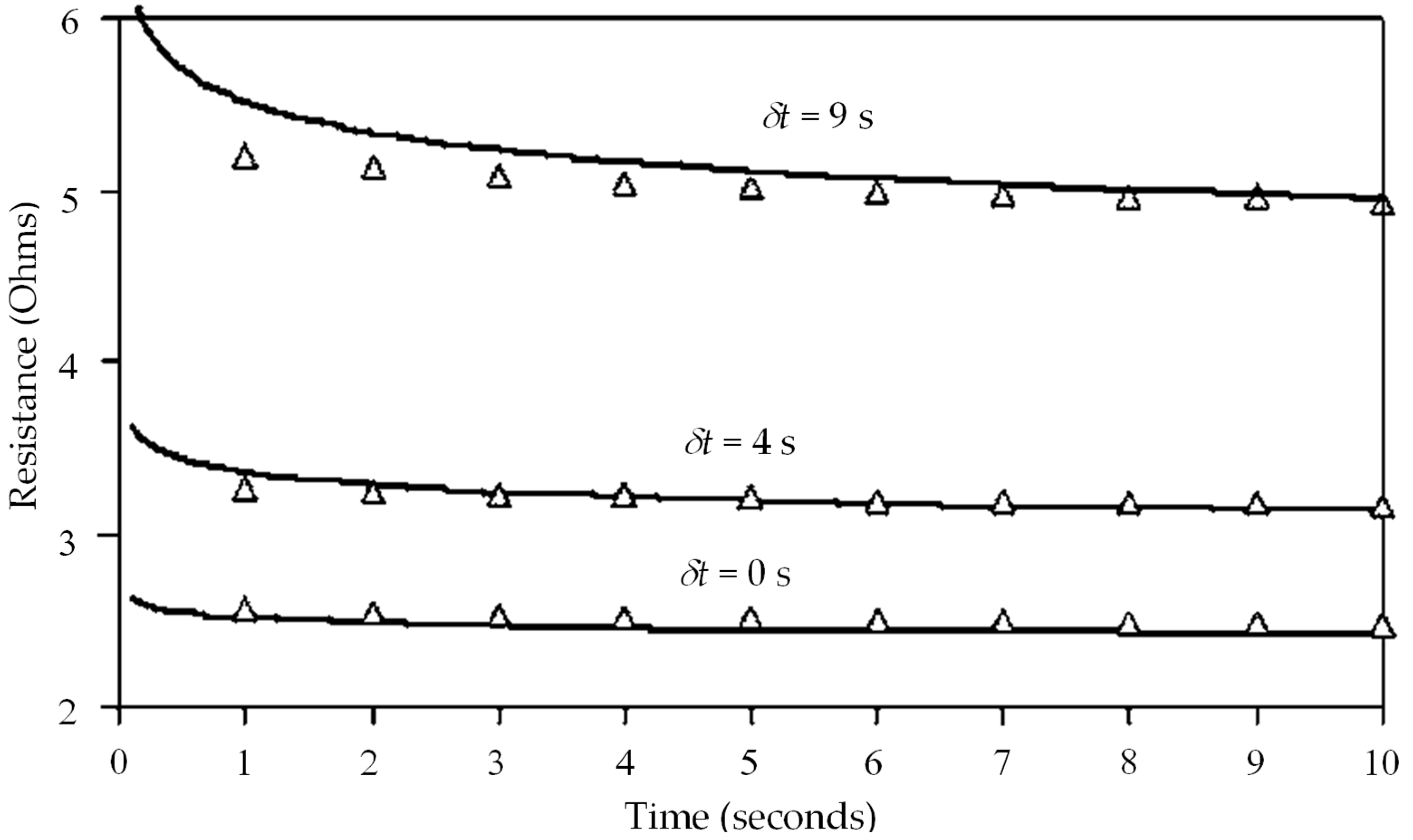
4.1. Effect of Asperity Deformations on Conductor Resistivity
4.2. Contact Area Expansion
5. Conclusions
Author Contributions
Funding
Conflicts of Interest
References
- Kanhere, O.; Rappaport, T.S. Position Location for Futuristic Cellular Communications: 5G and Beyond. IEEE Commun. Mag. 2021, 59, 70–75. [Google Scholar] [CrossRef]
- Saad, W.; Bennis, M.; Chen, M. A Vision of 6G Wireless Systems: Applications, Trends, Technologies, and Open Research Problems. IEEE Netw. 2020, 34, 134–142. [Google Scholar] [CrossRef] [Green Version]
- Giordani, M.; Polese, M.; Mezzavilla, M.; Rangan, S.; Zorzi, M. Toward 6G Networks: Use Cases and Technologies. IEEE Commun. Mag. 2020, 58, 55–61. [Google Scholar] [CrossRef]
- Rappaport, T.S.; Xing, Y.; Kanhere, O.; Ju, S.; Madanayake, A.; Mandal, S.; Alkhateeb, A.; Trichopoulos, G.C. Wireless Communications and Applications Above 100 GHz: Opportunities and Challenges for 6G and beyond. IEEE Access 2019, 7, 78729–78757. [Google Scholar] [CrossRef]
- Wei, T.; Feng, W.; Chen, Y.; Wang, C.-X.; Ge, N.; Lu, J. Hybrid Satellite-Terrestrial Communication Networks for the Maritime Internet of Things: Key Technologies, Opportunities, and Challenges. IEEE Internet Things J. 2021, 11, 8910–8934. [Google Scholar] [CrossRef]
- Kodheli, O.; Lagunas, E.; Maturo, N.; Sharma, S.K.; Shankar, B.; Montoya, J.F.M.; Duncan, J.C.M.; Spano, D.; Chatzinotas, S.; Kisseleff, S.; et al. Satellite Communications in the New Space Era: A Survey and Future Challenges. IEEE Commun. Surv. Tutor. 2021, 1, 70–109. [Google Scholar] [CrossRef]
- Alkendi, Y.; Seneviratne, L.; Zweiri, Y. State of the Art in Vision-Based Localization Techniques for Autonomous Navigation Systems. IEEE Access 2021, 9, 76847–76874. [Google Scholar] [CrossRef]
- Waheed, M.Z.; Korpi, D.; Anttila, L.; Kiayani, A.; Kosunen, M.; Stadius, K.; Campo, P.P.; Turunen, M.; Allén, M.; Ryynänen, J.; et al. Passive Intermodulation in Simultaneous Transmit–Receive Systems: Modeling and Digital Cancellation Methods. IEEE Trans. Microw. Theory Tech. 2020, 68, 3633–3652. [Google Scholar] [CrossRef]
- Kozlov, D.; Shitvov, A.P.; Bulja, S.; Lundy, R.; Rulikowski, P.; Nolan, K.; Enright, R. Practical Mitigation of Passive Intermodulation in Microstrip Circuits. IEEE Trans. Electromagn. Compat. 2020, 62, 163–172. [Google Scholar] [CrossRef]
- Zhang, S.; Zhao, X.; Cao, Z.; Zhang, K.; Gao, F.; He, Y. Experimental Study of Electrical Contact Nonlinearity and its Passive Intermodulation Effect. IEEE Trans. Comp. Packag. Manufact. Tech. 2020, 3, 424–434. [Google Scholar] [CrossRef]
- Gard, K.G.; Larson, L.E.; Steer, M.B. The impact of RF front-end characteristics on the spectral regrowth of communications signals. IEEE Trans. Microw. Theory Tech. 2005, 6, 2179–2186. [Google Scholar] [CrossRef]
- Grimm, M.; Allén, M.; Marttila, J.; Valkama, M.; Thomä, R. Joint Mitigation of Nonlinear RF and Baseband Distortions in Wideband Direct-Conversion Receivers. IEEE Trans. Microw. Theory Tech. 2014, 1, 166–182. [Google Scholar] [CrossRef]
- Vansebrouck, R.; Jabbour, C.; Jamin, O.; Desgreys, P. Fully-Digital Blind Compensation of Non-Linear Distortions in Wideband Receivers. IEEE Trans. Circ. Syst. I 2017, 8, 2112–2123. [Google Scholar] [CrossRef]
- Yang, P.; Xiao, Y.; Xiao, M.; Li, S. 6G Wireless Communications: Vision and Potential Techniques. IEEE Netw. 2019, 33, 70–75. [Google Scholar] [CrossRef]
- Zardi, F.; Nayeri, P.; Rocca, P.; Haupt, R. Artificial Intelligence for Adaptive and Reconfigurable Antenna Arrays: A Review. IEEE Antennas Propag. Mag. 2021, 3, 28–38. [Google Scholar] [CrossRef]
- Morales-Cespedes, M.; Vandendorpe, L.; Armada, A.G. Interference Management for K-Tier Networks without CSIT based on Reconfigurable Antennas. IEEE Trans. Commun. 2021, 69, 8068–8084. [Google Scholar] [CrossRef]
- Stauss, G.H. Intrinsic Sources of IM Generation; Naval Research Lab.: Washington, DC, USA, 1980; Chapter 5; pp. 65–82. [Google Scholar]
- Foord, A.P.; Rawlins, A.D. A Study of Passive Intermodulation Interference in Space RF Hardware; University of Kent at Canterbury: Canterbury, UK, 1992. [Google Scholar]
- Seron, D.; Collado, C.; Mateu, J.; O’Callaghan, J.M. Analysis and simulation of distributed nonlinearities in ferroelectrics and superconductors for microwave applications. IEEE Trans. Microw. Theory Tech. 2006, 3, 1154–1160. [Google Scholar] [CrossRef] [Green Version]
- Boyhan, J.W.; Henzing, H.F.; Koduru, C. Satellite passive intermodulation: Systems considerations. IEEE Trans. Aerosp. Electron. Syst. 1996, 3, 1058–1064. [Google Scholar] [CrossRef]
- Bolli, P.; Selleri, S.; Pelosi, G. Passive intermodulation on large reflector antennas. IEEE Antennas Propag. Mag. 2002, 5, 13–20. [Google Scholar] [CrossRef]
- Holm, R. The electric tunnel effect across thin insulator films in contacts. J. Appl. Phys. 1951, 5, 569–574. [Google Scholar] [CrossRef]
- Simmons, J.G. Generalized formula for the electric tunnel effect between similar electrodes separated by a thin insulating film. J. Appl. Phys. 1963, 6, 1793–1803. [Google Scholar] [CrossRef] [Green Version]
- Bond, C.D.; Guenzer, C.S.; Carosella, C.A. Intermodulation generation by electron tunneling through aluminum-oxide films. Proc. IEEE 1979, 12, 1643–1652. [Google Scholar] [CrossRef]
- Yamamoto, Y.; Kuga, N. Short-Circuit Transmission Line Method for PIM Evaluation of Metallic Materials. IEEE Trans. Electromagn. Compat. 2007, 3, 682–688. [Google Scholar] [CrossRef]
- Zhang, P. Scaling for quantum tunneling current in nano- and subnano-scale plasmonic junctions. Sci. Rep. 2015, 5, 9826. [Google Scholar] [CrossRef] [PubMed] [Green Version]
- Banerjee, S.; Zhang, P. A generalized self-consistent model for quantum tunneling current in dissimilar metal-insulator-metal junction. AIP Adv. 2019, 9, 085302. [Google Scholar] [CrossRef] [Green Version]
- Banerjee, S.; Luginsland, J.; Zhang, P. A two dimensional tunneling resistance transmission line model for nanoscale parallel electrical contacts. Sci. Rep. 2019, 9, 14484. [Google Scholar] [CrossRef]
- Banerjee, S.; Luginsland, J.; Zhang, P. Interface Engineering of Electrical Contacts. Phys. Rev. Appl. 2021, 15, 064048. [Google Scholar] [CrossRef]
- Auld, B.A.; Didomenico, M., Jr.; Pantell, R.H. Traveling-wave harmonic generation along nonlinear transmission lines. J. Appl. Phys. 1962, 12, 3537–3545. [Google Scholar] [CrossRef]
- Bayrak, M.; Benson, F. Intermodulation products from nonlinearities in transmission lines and connectors at microwave frequencies. Proc. IEE 1975, 4, 361–367. [Google Scholar] [CrossRef]
- Schuchinsky, A.G.; Francey, J.; Fusco, V.F. Distributed sources of passive intermodulation on printed lines. Proc. IEEE Antennas Propag. Soc. Int. Symp. 2005, 4B, 447–450. [Google Scholar] [CrossRef]
- Zelenchuk, D.E.; Shitvov, A.P.; Schuchinsky, A.G.; Fusco, V.F. Passive Intermodulation in Finite Lengths of Printed Microstrip Lines. IEEE Trans. Microw. Theory Tech. 2008, 11, 2426–2434. [Google Scholar] [CrossRef]
- Shitvov, A.P.; Zelenchuk, D.E.; Schuchinsky, A.G.; Fusco, V.F. Passive Intermodulation Generation on Printed Lines: Near-Field Probing and Observations. IEEE Trans. Microw. Theory Tech. 2008, 12, 3121–3128. [Google Scholar] [CrossRef]
- Mateu, J.; Collado, C.; Orloff, N.; Booth, J.; Rocas, E.; Padilla, A.; O’Callaghan, J. Third-order intermodulation distortion and harmonic generation in mismatched weakly nonlinear transmission lines. IEEE Trans. Microw. Theory Tech. 2009, 57, 10–18. [Google Scholar] [CrossRef] [Green Version]
- Wilkerson, J.R.; Lam, P.G.; Gard, K.G.; Steer, M.B. Distributed passive intermodulation distortion on transmission lines. IEEE Trans. Microw. Theory Tech. 2011, 5, 1190–1205. [Google Scholar] [CrossRef]
- Wilkerson, J.R.; Gard, K.G.; Schuchinsky, A.G.; Steer, M.B. Electro-thermal theory of intermodulation distortion in lossy microwave components. IEEE Trans. Microw. Theory Tech. 2008, 12, 2717–2725. [Google Scholar] [CrossRef]
- Jin, Q.; Gao, J.; Flowers, G.T.; Wu, Y.; Huang, H. Passive Intermodulation Models of Current Distortion in Electrical Contact Points. IEEE Microw. Wirel. Comp. Lett. 2019, 3, 180–182. [Google Scholar] [CrossRef]
- Jin, Q.; Gao, J.; Bi, L.; Zhou, Y. The Impact of Contact Pressure on Passive Intermodulation in Coaxial Connectors. IEEE Microw. Wirel. Comp. Lett. 2020, 2, 177–180. [Google Scholar] [CrossRef]
- Chen, X.; Wang, L.; Pommerenke, D.; Yu, M. Passive Intermodulation on Coaxial Connector Under Electro-Thermal-Mechanical Multiphysics. IEEE Trans. Microw. Theory Tech. 2022, 70, 169–177. [Google Scholar] [CrossRef]
- Hienonen, S.; Vainikainen, P.; Raisanen, A.V. Sensitivity measurements of a passive intermodulation near-field scanner. IEEE Antennas Propag. Mag. 2003, 4, 124–129. [Google Scholar] [CrossRef]
- Wilkerson, J.R.; Kilgore, I.M.; Gard, K.G.; Steer, M.B. Passive Intermodulation Distortion in Antennas. IEEE Trans. Antennas Propag. 2015, 2, 474–482. [Google Scholar] [CrossRef]
- Wang, M.; Kilgore, I.M.; Steer, M.B.; Adams, J.J. Characterization of Intermodulation Distortion in Reconfigurable Liquid Metal Antennas. IEEE Antennas Wirel. Propag. Lett. 2018, 2, 279–282. [Google Scholar] [CrossRef]
- Wu, D.; Xie, Y.; Kuang, Y.; Niu, L. Prediction of Passive Intermodulation on Mesh Reflector Antenna Using Collaborative Simulation: Multiscale Equivalent Method and Nonlinear Model. IEEE Trans. Antennas Propag. 2018, 3, 1516–1521. [Google Scholar] [CrossRef]
- Yong, S.; Yang, S.; Zhang, L.; Chen, X.; Pommerenke, D.J.; Khilkevich, V. Passive Intermodulation Source Localization Based on Emission Source Microscopy. IEEE Trans. Electromagn. Compat. 2020, 1, 266–271. [Google Scholar] [CrossRef]
- Wilcox, J.; Molmud, P. Thermal Heating Contribution to Intermodulation Fields in Coaxial Waveguides. IEEE Trans. Commun. 1976, 2, 238–243. [Google Scholar] [CrossRef]
- Steer, M.B.; Williamson, T.G.; Wetherington, J.; Wilkerson, J.; Aaen, P.; Schuchinsky, A.G. Power and temperature dependence of passive intermodulation distortion. In Proceedings of the 22nd International Microwave and Radar Conference (MIKON), Poznan, Poland, 14–17 May 2018; pp. 428–431. [Google Scholar] [CrossRef]
- Guo, X.; Jackson, D.R.; Koledintseva, M.Y.; Hinaga, S.; Drewniak, J.L.; Chen, J. An analysis of conductor surface roughness effects on signal propagation for stripline interconnects. IEEE Trans. Electromagn. Compat. 2014, 3, 707–714. [Google Scholar] [CrossRef]
- Ansuinelli, P.; Schuchinsky, A.G.; Frezza, F.; Steer, M.B. Passive intermodulation due to conductor surface roughness. IEEE IEEE Trans. Microw. Theory Tech. 2018, 2, 688–699. [Google Scholar] [CrossRef]
- Rezvanian, O.; Zikry, M.A.; Brown, C.; Krim, J. Surface roughness, asperity contact and gold RF MEMS switch behavior. J. Micromech. Microeng. 2007, 10, 2006–2015. [Google Scholar] [CrossRef] [Green Version]
- Jackson, R.L.; Streator, J.L. A multi-scale model for contact between rough surfaces. Wear 2006, 11–12, 1337–1347. [Google Scholar] [CrossRef]
- Jackson, R.L.; Crandall, E.R.; Bozack, M.J. Rough surface electrical contact resistance considering scale dependent properties and quantum effects. J. Appl. Phys. 2015, 117, 195101. [Google Scholar] [CrossRef]
- Zhai, C.; Hanaor, D.; Proust, G.; Brassart, L.; Gan, Y. Stress-dependent electrical contact resistance at fractal rough surfaces. J. Eng. Mech. 2017, 3, B4015001. [Google Scholar] [CrossRef]
- Vicente, C.; Hartnagel, H.L. Passive-intermodulation analysis between rough rectangular waveguide flanges. Microw. Theory Tech. 2005, 8, 2515–2525. [Google Scholar] [CrossRef]
- Yang, H.; Zhu, L.; Gao, F.; Fan, J.; Wen, H. Measurement and analysis of passive intermodulation induced by additional impedance in loose contact coaxial connector. IEEE Trans. Electromagn. Compat. 2019, 6, 1876–1883. [Google Scholar] [CrossRef]
- Zhang, K.; Li, T.; Jiang, J. Passive intermodulation of contact nonlinearity on microwave connectors. IEEE Trans. Electromagn. Compat. 2018, 2, 513–519. [Google Scholar] [CrossRef]
- Jin, Q.; Gao, J.; Flowers, G.T.; Wu, Y.; Xie, G. Modeling of passive intermodulation with electrical contacts in coaxial connectors. IEEE Trans. Microw. Theory Tech. 2018, 9, 4007–4016. [Google Scholar] [CrossRef]
- Chen, X.; He, Y.; Yu, M.; Pommerenke, D.J.; Fan, J. Empirical Modeling of Contact Intermodulation Effect on Coaxial Connectors. IEEE Trans. Instrum. Meas. 2020, 7, 5091–5099. [Google Scholar] [CrossRef]
- Chen, X.; He, Y.; Yang, S.; Cui, W.; Zhang, Y.-J.; Pommerenke, D.J.; Fan, J. Analytic passive intermodulation behavior on the coaxial connector using Monte Carlo approximation. IEEE Trans. Electromagn. Compat. 2018, 5, 1207–1214. [Google Scholar] [CrossRef]
- Kogut, L.; Komvopoulos, K. Analytical current-voltage relationships for electron tunneling across rough interfaces. J. Appl. Phys. 2005, 97, 073701. [Google Scholar] [CrossRef]
- Nikolic, B.; Allen, P.B. Electron Transport through a circular constriction. Phys. Rev. B 1999, 6, 3963–3969. [Google Scholar] [CrossRef] [Green Version]
- Sharvin, Y.V. On the possible method for studying Fermi surfaces. Sov. Phys. JETP 1965, 21, 655–656. [Google Scholar]
- Jensen, B.D.; Chow, L.L.-W.; Huang, K.; Saitou, K.; Volakis, J.L.; Kurabayashi, K. Effect of nanoscale heating on electrical transport in RF MEMS switch contacts. J. Microelectromechanical Syst. 2005, 5, 935–946. [Google Scholar] [CrossRef] [Green Version]
- Kogut, L.; Komvopoulos, K. Electrical contact resistance theory for conductive rough surfaces separated by a thin insulating film. J. Appl. Phys. 2004, 2, 576–585. [Google Scholar] [CrossRef]
- Miller, C.W.; Li, Z.-P.; Åkerman, J.; Schuller, I.K. Impact of interfacial roughness on tunneling conductance and extracted barrier parameters. Appl. Phys. Lett. 2007, 90, 043513. [Google Scholar] [CrossRef]
- Brinkman, W.F.; Dynes, R.C.; Rowell, J.M. Tunneling Conductance of Asymmetrical Barriers. J. Appl. Phys. 1970, 41, 1915–1921. [Google Scholar] [CrossRef] [Green Version]
- Crinon, E.; Evans, J.T. The effect of surface roughness, oxide film thickness and interfacial sliding on the electrical contact resistance of aluminium. Mater. Sci. Eng. A 1998, 1–2, 121–128. [Google Scholar] [CrossRef]
- Go, D.B.; Haase, J.R.; George, J.; Mannhart, J.; Wanke, R.; Nojeh, A.; Nemanich, R. Thermionic energy conversion in the twenty-first century: Advances and Opportunities for Space and Terrestrial Applications. Front. Mech. Eng. 2017, 3, 13. [Google Scholar] [CrossRef] [Green Version]
- Jin, Q.; Gao, J.; Flowers, G.T.; Wu, Y.; Xie, G.; Bi, L. Effects of environmental temperature on passive intermodulation in electrical connectors. IEEE Trans. Compon. Packag. Manufact. Tech. 2020, 12, 2008–2017. [Google Scholar] [CrossRef]
- Rocas, E.; Collado, C.; Mateu, J.; Orloff, N.; O’Callaghan, J.M.; Booth, J.C. A large-signal model of ferroelectric thin-film transmission lines. IEEE Trans. Microw. Theory Tech. 2011, 12, 3059–3067. [Google Scholar] [CrossRef]
- Rezvanian, O.; Brown, C.; Zikry, M.A.; Kingon, A.I.; Krim, J.; Irving, D.L.; Brenner, D.W. The role of creep in the time-dependent resistance of Ohmic gold contacts in radio frequency microelectromechanical system devices. J. Appl. Phys. 2008, 104, 024513. [Google Scholar] [CrossRef]
- Zikry, M.A. An accurate and stable algorithm for high strain-rate finite strain plasticity. Comput. Struct. 1994, 3, 337–350. [Google Scholar] [CrossRef]
- Hyman, D.; Mehregany, M. Contact physics of gold microcontacts for MEMS switches. IEEE Trans. Compon. Packag. Technol. 1999, 22, 357–364. [Google Scholar] [CrossRef]
- Holm, R. Electric Contacts: Theory and Applications, 4th ed.; Springer: Berlin, Germany, 1967. [Google Scholar]


Publisher’s Note: MDPI stays neutral with regard to jurisdictional claims in published maps and institutional affiliations. |
© 2022 by the authors. Licensee MDPI, Basel, Switzerland. This article is an open access article distributed under the terms and conditions of the Creative Commons Attribution (CC BY) license (https://creativecommons.org/licenses/by/4.0/).
Share and Cite
Dayan, A.; Huang, Y.; Schuchinsky, A. Passive Intermodulation at Contacts of Rough Conductors. Electron. Mater. 2022, 3, 65-81. https://doi.org/10.3390/electronicmat3010007
Dayan A, Huang Y, Schuchinsky A. Passive Intermodulation at Contacts of Rough Conductors. Electronic Materials. 2022; 3(1):65-81. https://doi.org/10.3390/electronicmat3010007
Chicago/Turabian StyleDayan, Amir, Yi Huang, and Alex Schuchinsky. 2022. "Passive Intermodulation at Contacts of Rough Conductors" Electronic Materials 3, no. 1: 65-81. https://doi.org/10.3390/electronicmat3010007