
p-Type Iodine-Doping of Cu3N and Its Conversion to γ-CuI for the Fabrication of γ-CuI/Cu3N p-n Heterojunctions

 and
and
Abstract
:
1. Introduction
2. Materials and Methods
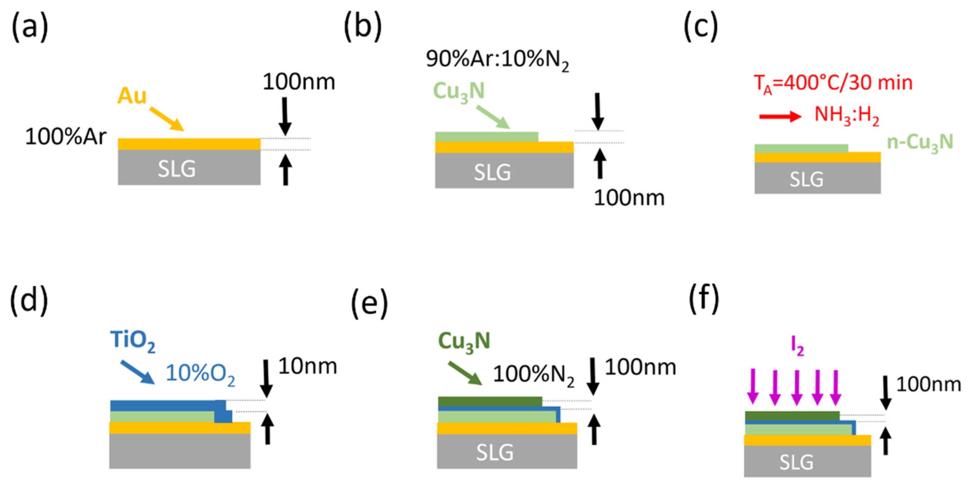
2.1. Experimental Proceedure
2.2. Theoretical
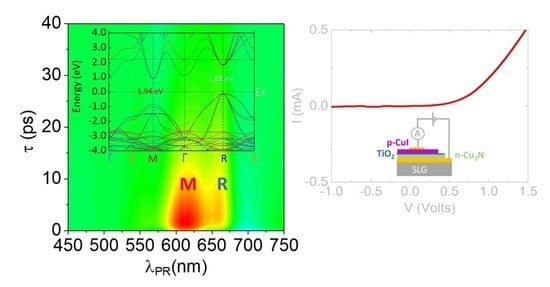
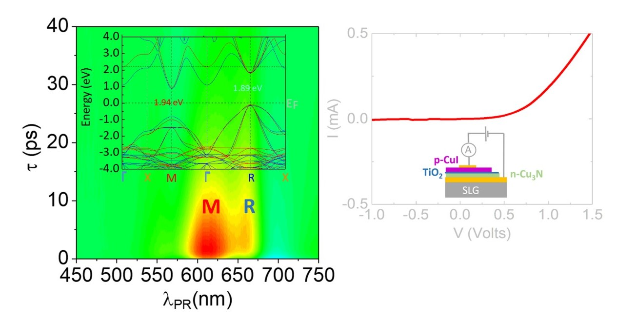
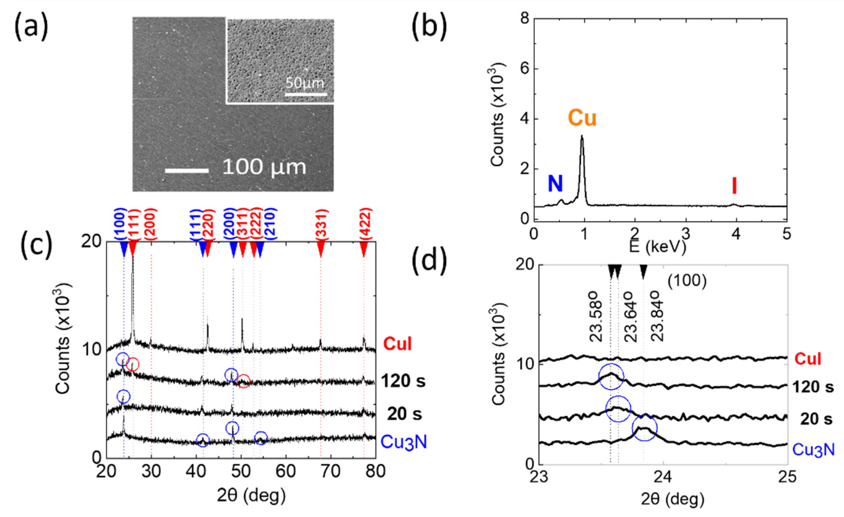
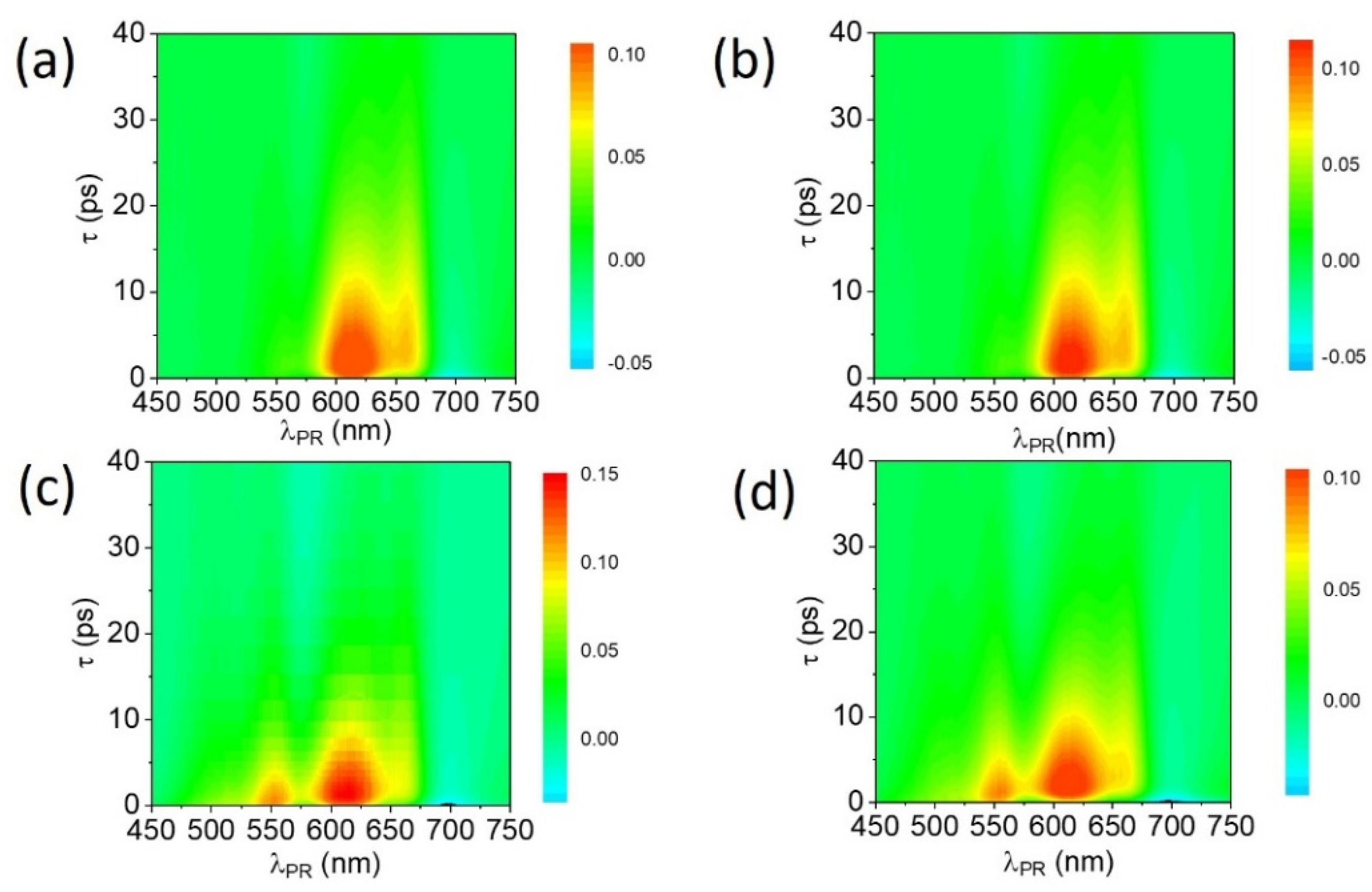
3. Results
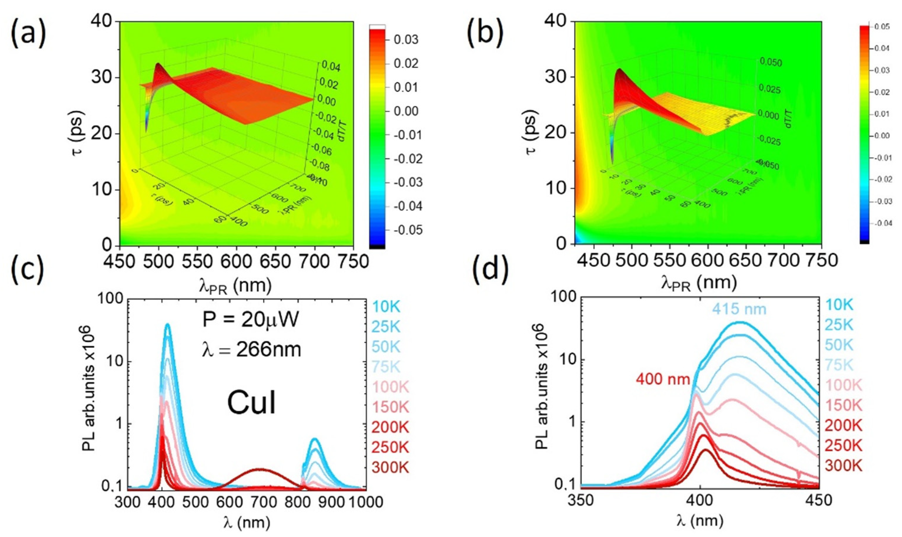
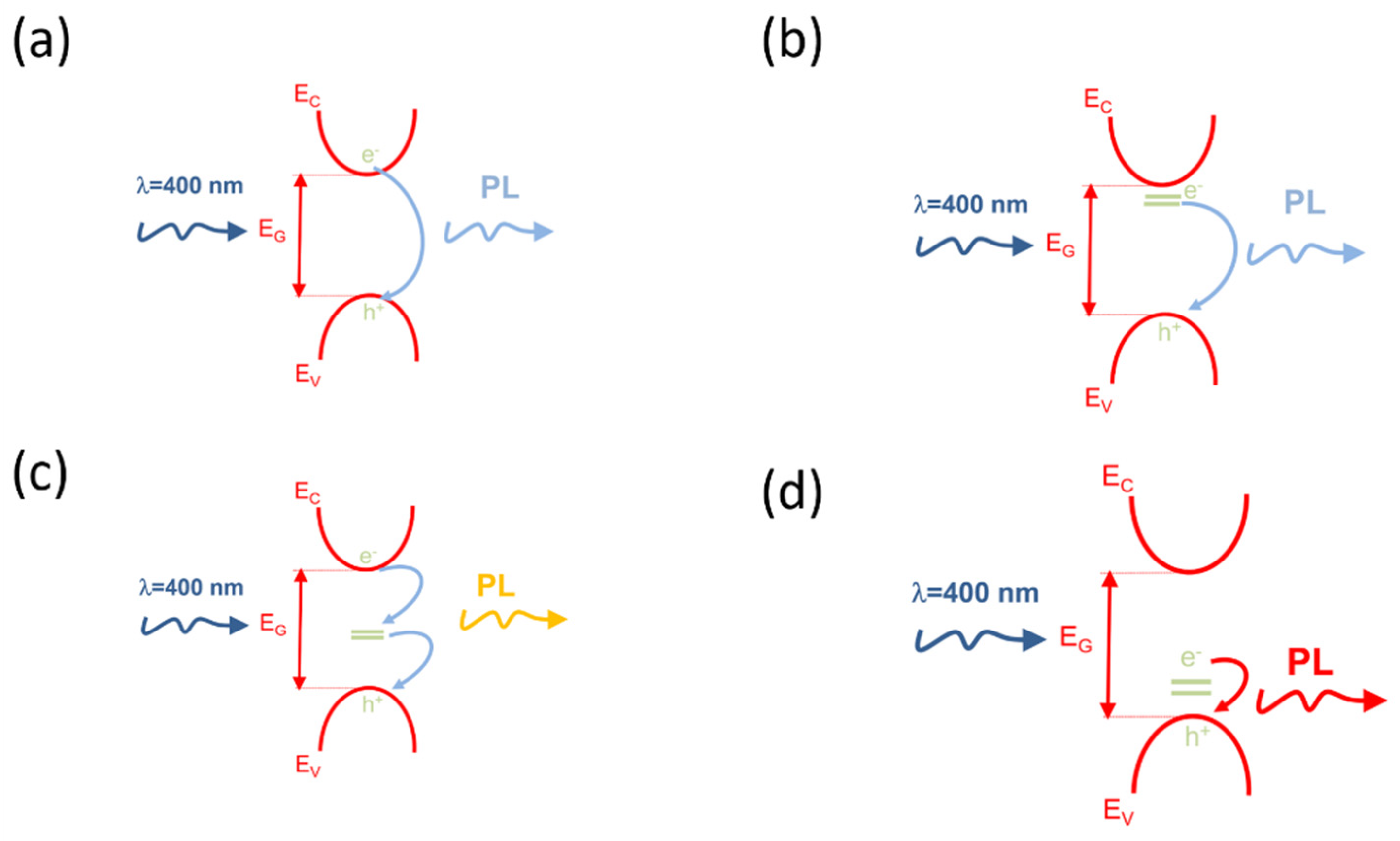
3.1. Structural, Electrical and Optical Properties of p-Type I: Cu3N and γ-CuI
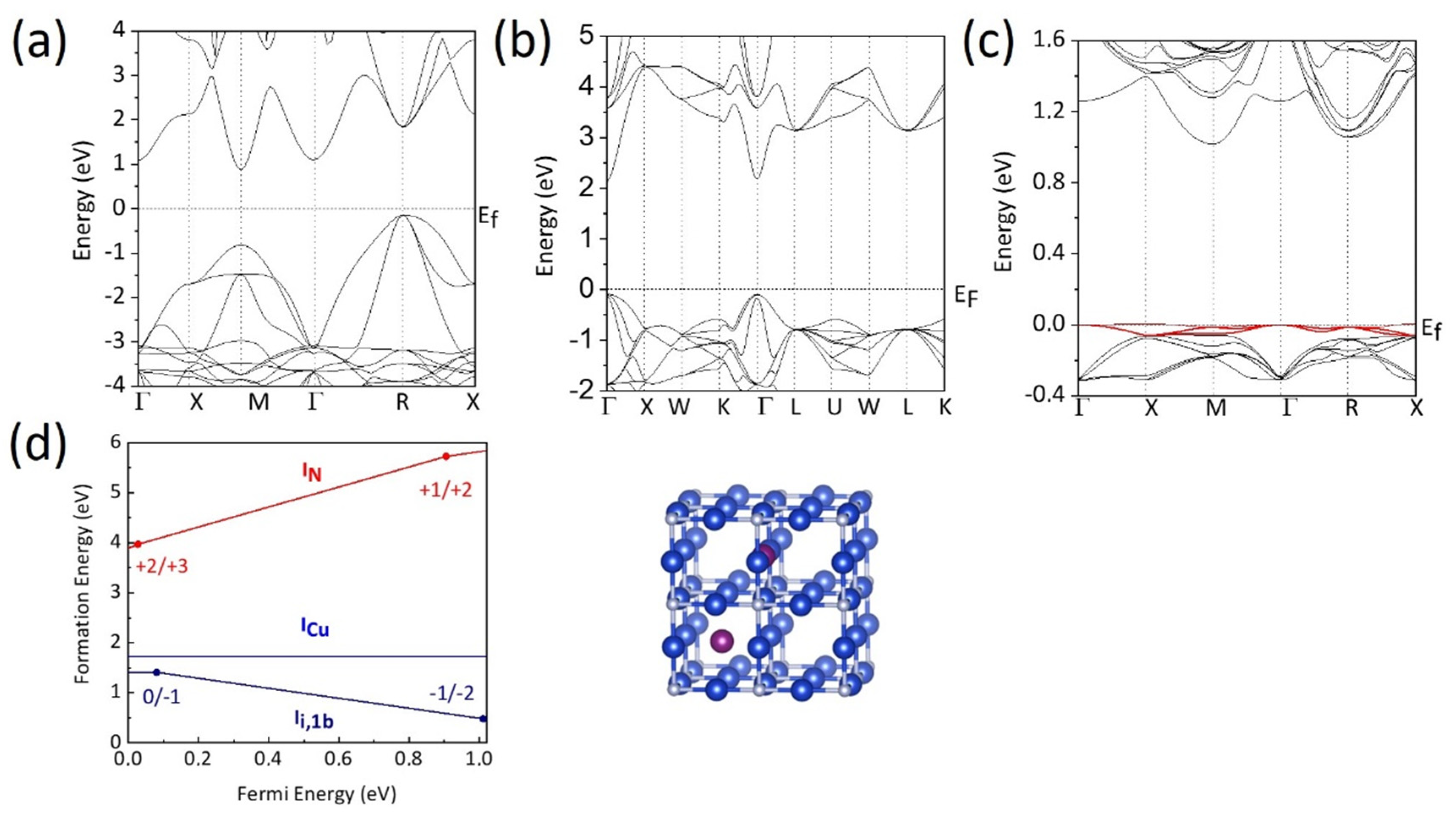
3.2. DFT Electronic Band Structure Calculations
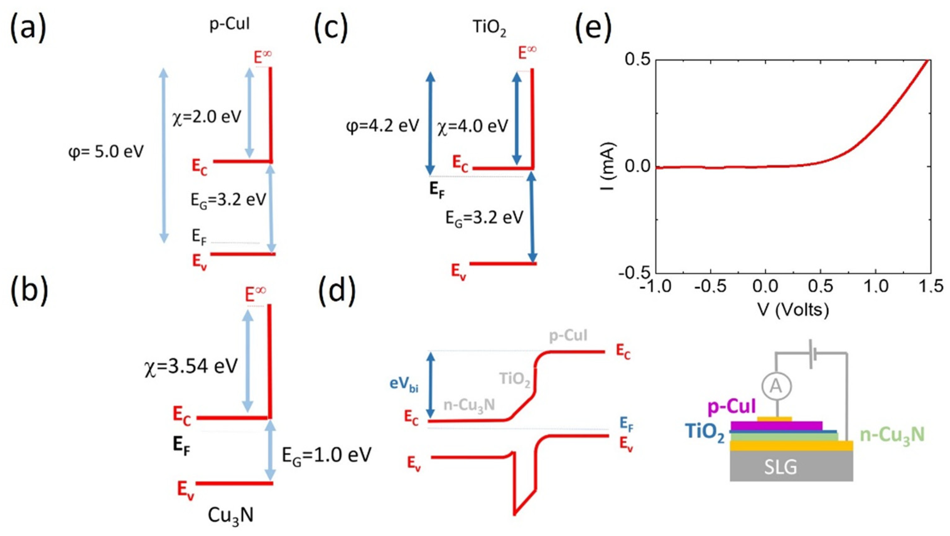
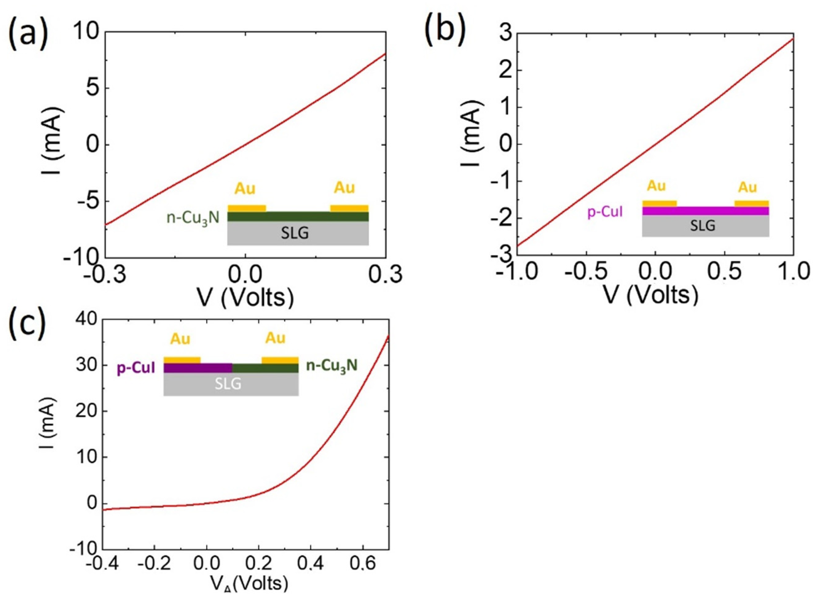
3.3. γ-CuI/TiO2/Cu3N and γ-CuI/Cu3N p-n Heterojunctions
4. Conclusions
Author Contributions
Funding
Conflicts of Interest
References
- Zakutayev, A.; Caskey, C.M.; Fioretti, A.N.; Ginley, D.S.; Vidal, J.; Stevanovic, V.; Tea, E.; Lany, S. Defect Tolerant Semiconductors for Solar Energy Conversion. J. Phys. Chem. Lett. 2014, 5, 1117–1125. [Google Scholar] [CrossRef] [PubMed]
- Dongsoo, L.; Seho, S.; Jiseok, K.; Hyunjung, P.; Minchul, J.; Eunkyung, P.; Byoungkuk, S.; Yeongil, J.; Taeseup, S.; Ungyu, P. Copper Nitride Nanowires Printed Li with Stable Cycling for Li Metal Batteries in Carbonate Electrolytes. Adv. Mater. 2020, 32, 1905573. [Google Scholar]
- Birkett, M.; Savory, C.N.; Fioretti, A.N.; Thompson, P.; Muryn, C.A.; Weerakkody, A.D.; Mitrovic, I.Z.; Hall, S.; Treharne, R.; Dhanak, V.R.; et al. Atypically small temperature-dependence of the direct band gap in the metastable semiconductor copper nitrideCu3N. Phys. Rev. B 2017, 95, 115201. [Google Scholar] [CrossRef] [Green Version]
- Matsuzaki, K.; Harada, K.; Kumagai, Y.; Koshiya, S.; Kimoto, K.; Ueda, S.; Sasase, M.; Maeda, A.; Susaki, T.; Kitano, M.; et al. High-Mobility p-Type and n-Type Copper Nitride Semiconductors by Direct Nitriding Synthesis and In Silico Doping Design. Adv. Mater. 2018, 30, e1801968. [Google Scholar] [CrossRef]
- Zervos, M.; Othonos, A.; Sergides, M.; Pavloudis, T.; Kioseoglou, J. Observation of the Direct Energy Band Gaps of Defect-Tolerant Cu3N by Ultrafast Pump-Probe Spectroscopy. J. Phys. Chem. C 2020, 124, 3459–3469. [Google Scholar] [CrossRef]
- Nikam, R.D.; Kwak, M.; Lee, J.; Rajput, K.G.; Banerjee, W.; Hwang, H. Near ideal synaptic functionalities in Li ion synaptic transistor using Li3POxSex electrolyte with high ionic conductivity. Sci. Rep. 2019, 9, 1–11. [Google Scholar] [CrossRef] [Green Version]
- Kozen, A.C.; Pearse, A.J.; Lin, C.-F.; Noked, M.; Rubloff, G.W. Atomic Layer Deposition of the Solid Electrolyte LiPON. Chem. Mater. 2015, 27, 5324–5331. [Google Scholar] [CrossRef] [Green Version]
- Yamada, N.; Ino, R.; Ninomiya, Y. Truly Transparent p-Type γ-CuI Thin Films with High Hole Mobility. Chem. Mater. 2016, 28, 4971–4981. [Google Scholar] [CrossRef]
- Yamada, N.; Kondo, Y.; Ino, R. Low-Temperature Fabrication and Performance of Polycrystalline CuI Films as Transparent p-Type Semiconductors. Phys. Status Solidi 2019, 216, 1700782. [Google Scholar] [CrossRef]
- Sepalage, G.A.; Meyer, S.; Pascoe, A.; Scully, A.D.; Huang, F.; Bach, U.; Cheng, Y.B.; Spiccia, L. Copper(I) Iodide as Hole-Conductor in Planar Perovskite Solar Cells: Probing the Origin of J–V Hysteresis. Adv. Funct. Mater. 2015, 25, 5650–5661. [Google Scholar] [CrossRef]
- Sun, W.; Peng, H.; Li, Y.; Yan, W.; Liu, Z.; Bian, Z.; Huang, C. Solution-Processed Copper Iodide as an Inexpensive and Effective Anode Buffer Layer for Polymer Solar Cells. J. Phys. Chem. C 2014, 118, 16806–16812. [Google Scholar] [CrossRef]
- Zainun, A.R.; Mamat, M.H.; Noor, U.M.; Rusop, M. Particles Size and Conductivity Study of P-Type Copper (I) Iodide (CuI) Thin Film for Solid State Dye-Sensitized Solar Cells. IOP Conf. Ser. Mater. Sci. Eng. 2011, 17, 012009. [Google Scholar] [CrossRef]
- Jeona, K.; Jeea, H.; Parka, M.J.; Limb, S.; Jeonga, C. Characterization of the Copper Iodide Hole-Selective Contact for Silicon Solar Cell Application. Thin Solid Films 2018, 660, 613–617. [Google Scholar] [CrossRef]
- Luo, W.; Zeng, C.; Du, X.; Leng, C.; Yao, W.; Shi, H.; Wei, X.; Du, C.; Lu, S. Copper thiocyanate/copper iodide based hole transport composites with balanced properties for efficient polymer light-emitting diodes. J. Mater. Chem. C 2018, 6, 4895–4902. [Google Scholar] [CrossRef]
- Choi, C.-H.; Gorecki, J.Y.; Fang, Z.; Allen, M.; Li, S.; Lin, L.-Y.; Cheng, C.-C.; Chang, C.-H. Low-temperature, inkjet printed p-type copper(I) iodide thin film transistors. J. Mater. Chem. C 2016, 4, 10309–10314. [Google Scholar] [CrossRef]
- Bai, S.-Q.; Wong, I.H.K.; Lin, M.; Young, D.J.; Hor, T.S.A. A thermoelectric copper-iodide composite from the pyrolysis of a well-defined coordination polymer. Dalton Trans. 2018, 47, 5564–5569. [Google Scholar] [CrossRef] [PubMed]
- Revan, D.N.; Ashok, S.P.; Sankar, R.; Chen, Y.T. Epitaxial Growth of Vertically Stacked p-MoS2/n-MoS2. Nano Energy 2017, 32, 454–462. [Google Scholar]
- Bartolomeo, A. Emerging 2D Materials and Their Van Der Waals Heterostructures. Nanomaterials 2020, 10, 579. [Google Scholar] [CrossRef] [Green Version]
- Gibertini, M.; Koperski, M.; Morpurgo, A.F.; Novoselov, K.S. Magnetic 2D Materials and Heterostructures. Nat. Nanotechnol. 2019, 14, 408. [Google Scholar] [CrossRef] [PubMed] [Green Version]
- Chen, S.-C.; Huang, S.-Y.; Sakalley, S.; Paliwal, A.; Chen, Y.-H.; Liao, M.-H.; Sun, H.; Biring, S. Optoelectronic properties of Cu3N thin films deposited by reactive magnetron sputtering and its diode rectification characteristics. J. Alloys Compd. 2019, 789, 428–434. [Google Scholar] [CrossRef]
- Yee, Y.S.; Inoue, H.; Hultqvist, A.; Hanifi, D.; Salleo, A.; Magyari-Köpe, B.; Nishi, Y.; Bent, S.F.; Clemens, B.M. Copper interstitial recombination centers in Cu3N. Phys. Rev. B 2018, 97, 245201. [Google Scholar] [CrossRef] [Green Version]
- Yu, A.; Hu, R.; Liu, W.; Zhang, R.; Zhang, J.; Pu, Y.; Chu, L.; Yang, J.; Li, X. Preparation and characterization of Mn doped copper nitride films with high photocurrent response. Curr. Appl. Phys. 2018, 18, 1306–1312. [Google Scholar] [CrossRef]
- Kresse, G.; Furthmüller, G. Efficiency of Ab-Initio Total Energy Calculations for Metals and Semiconductors Using a Plane-Wave Basis Set. Comput. Mater. Sci. 1996, 6, 15–50. [Google Scholar] [CrossRef]
- Kresse, G.; Furthmüller, G. Efficient Iterative Schemes for Ab Initio Total-Energy Calculations Using a Plane-Wave Basis Set. Phys. Rev. B 1996, 54, 11169. [Google Scholar] [CrossRef] [PubMed]
- Blochl, P.E. Projector Augmented-Wave Method. Phys. Rev. B 1994, 50, 17953. [Google Scholar] [CrossRef] [PubMed] [Green Version]
- Kresse, G.; Joubert, D. From Ultra Soft Pseudopotentials to the Projector Augmented-Wave Method. Phys. Rev. B 1999, 59, 1758–1775. [Google Scholar] [CrossRef]
- Perdew, J.P.; Burke, K.; Ernzerhof, M. Generalized gradient approximation made simple. Phys. Rev. Lett. 1997, 77, 3865–3868. [Google Scholar] [CrossRef] [PubMed] [Green Version]
- Dudarev, S.L.; Botton, G.A.; Savrasov, S.Y.; Humphreys, C.J.; Sutton, A.P. Electron-energy-loss spectra and the structural stability of nickel oxide: An LSDA+U study. Phys. Rev. B 1998, 57, 1505–1509. [Google Scholar] [CrossRef]
- Freysoldt, C.; Grabowski, B.; Hickel, T.; Neugebauer, J.; Kresse, G.; Janotti, A.; Van de Walle, C.G. First-principles calculations for point defects in solids. Rev. Mod. Phys. 2014, 86, 253–305. [Google Scholar] [CrossRef]
- Zervos, M.; Othonos, A.; Pavloudis, T.; Giaremis, S.; Kioseoglou, J.; Mavridou, K.; Katsikini, M.; Pinakidou, F.; Paloura, E.C. Impact of Oxygen on the Properties of Cu3N and Cu3−xN1−xOx. J. Phys. Chem. C 2021, 125, 3680–3688. [Google Scholar] [CrossRef]
- Peng, Y.; Yaacobi-Gross, N.; Perumal, A.K.; Faber, H.; Vourlias, G.; Patsalas, P.A.; Bradley, D.D.C.; He, Z.; Anthopoulos, T. Efficient organic solar cells using copper(I) iodide (CuI) hole transport layers. Appl. Phys. Lett. 2015, 106, 243302. [Google Scholar] [CrossRef] [Green Version]
- Gotoha, K.; Cuia, M.; Takahashia, I.; Kurokawaa, Y.; Usamia, N. Development of Spin-Coated Copper Iodide on Silicon for use in Hole-Selective Contacts. Energy Procedia 2017, 124, 598–603. [Google Scholar] [CrossRef]
- Kumarasinghe, A.R.; Flavell, W.R.; Thomas, A.G.; Mallick, A.K.; Tsoutsou, D.; Chatwin, C.; Rayner, S.; Kirkham, P.; Warren, S.; Patel, S.; et al. Electronic Properties of the Interface between p-CuI and Anatase-Phase n-TiO2 Single Crystal and Nanoparticulate Surfaces: A Photoemission Study. J. Chem. Phys. 2007, 127, 114703. [Google Scholar] [CrossRef] [PubMed]


Publisher’s Note: MDPI stays neutral with regard to jurisdictional claims in published maps and institutional affiliations. |
© 2022 by the authors. Licensee MDPI, Basel, Switzerland. This article is an open access article distributed under the terms and conditions of the Creative Commons Attribution (CC BY) license (https://creativecommons.org/licenses/by/4.0/).
Share and Cite
Tilemachou, A.; Zervos, M.; Othonos, A.; Pavloudis, T.; Kioseoglou, J. p-Type Iodine-Doping of Cu3N and Its Conversion to γ-CuI for the Fabrication of γ-CuI/Cu3N p-n Heterojunctions. Electron. Mater. 2022, 3, 15-26. https://doi.org/10.3390/electronicmat3010002
Tilemachou A, Zervos M, Othonos A, Pavloudis T, Kioseoglou J. p-Type Iodine-Doping of Cu3N and Its Conversion to γ-CuI for the Fabrication of γ-CuI/Cu3N p-n Heterojunctions. Electronic Materials. 2022; 3(1):15-26. https://doi.org/10.3390/electronicmat3010002
Chicago/Turabian StyleTilemachou, Argyris, Matthew Zervos, Andreas Othonos, Theodoros Pavloudis, and Joseph Kioseoglou. 2022. "p-Type Iodine-Doping of Cu3N and Its Conversion to γ-CuI for the Fabrication of γ-CuI/Cu3N p-n Heterojunctions" Electronic Materials 3, no. 1: 15-26. https://doi.org/10.3390/electronicmat3010002