Article

Structural and Electronic Properties of Small Perovskite Nanoparticles of the Form ABX3 (A = MA, DEA, FA, GA, B = Pb, Sn, X = Cl, Br, I)

by
Christos S. Garoufalis
1,*,
Iosif Galanakis
1,*,
Zaiping Zeng
2,
David B. Hayrapetyan
3 and
Sotirios Baskoutas
1,4
1
Department of Materials Science, Univesity of Patras, 265 04 Patras, Greece
2
Key Laboratory for Special Functional Materials of Ministry of Education, Collaborative Innovation Center of Nano Functional Materials and Applications, School of Materials Science and Engineering, Henan University, Kaifeng 475001, China
3
Institute of Engineering and Physics, Russian-Armenian University, Yerevan 0051, Armenia
4
Institut für Physikalische Chemie, Universität Hamburg, Grindelallee 117, 20146 Hamburg, Germany
*
Authors to whom correspondence should be addressed.
Electron. Mater. 2021, 2(3), 382-393; https://doi.org/10.3390/electronicmat2030026
Submission received: 29 June 2021 / Revised: 5 August 2021 / Accepted: 6 August 2021 / Published: 10 August 2021
(This article belongs to the Special Issue Feature Papers of Electronic Materials)

Abstract

:
Using a combination of first principles and semiempirical calculation, we explore the structural, electronic, and optical properties of a wide range of perovskite ( A B X 3 ) nanoparticle of different size and composition. The variations of the B X 3 backbone structure considered include all possible combinations of the cations B = P b , S n and the anions X = C l , B r , I , while the interstitial cation A is either methylamonium (MA), or formamidinium (FA), or guanidine amine (GA), or dimethylamine (DEA). Our results indicate that the orientational disorder of the A moieties may affect the structural and electronic properties of the NPs while the optical properties exhibit a clear dependence on the NPs’ size and the types of B cations and X anions, but they are quite insensitive to the type of A cation.

1. Introduction

Perovskites is a well-known and widely studied family of materials with a variety of applications in everyday life. The early perovskite materials had the general structure of A B O 3 . A had to be a cation of +2 valence and B a cation of +4 valence in order to achieve charge neutrality [1]. It seems that in nature the chemical formula A B X 3 is pretty stable and thus several materials crystallizing in this structure have been identified. Of particular interest are the ones where X is a halogen atom (Cl, Br or I) instead of oxygen which are widely known as halide perovskites [2,3,4]. In order to achieve charge neutrality in the case of halide perovskites, A has to be a monovalent cation and B a divalent cation. In the case where A is an organic molecule, the resulting materials are known as hybrid or organometallic halide perovskites [5]. The prototype material in the family of hybrid halide perovskites is M A P b I 3 , where MA stands for the methylammonium cation C H 3 N H 3 + . The interest of M A P b I 3 stems from its high charge-carrier mobility and its absorption at optical regime [5,6,7,8,9,10,11,12,13,14,15].
Hybrid halide perovskites find a variety of applications in several technological fields like optoelectronics [16], catalysis [17], and photovoltaics [2,3,5]. The most active field for applications is solar cells where S i has dominated for the last 60 years [18]. Although M A P b I 3 is the material of choice for photovoltaic applications [19,20], there is intense interest in the synthesis of new lead-free halide perovskites for such applications [4]. The interest in these materials for solar cells is so intense that several reviews appear in the literature every year [21,22,23,24,25,26,27].
Although most of the studies refer to bulk hybrid halide perovskites, the development of nanotechnology also increased the interest in nanostructures with a size smaller than 10 nm like quantum dots (QDs), nanoparticles (NPs), nanowires, nanorods, etc. Such nanostructures find applications in devices where quantum-mechanics governs the physical properties like light emitting diodes (LED) [2]. There are several experimental studies on the synthesis and properties of perovskite nanostructures focusing on particular materials like M A P b B r 3 and M A P b I 3 [2,3,5,6,28,29,30,31,32,33,34,35,36]. In general, in experiments, the perovskite QDs prefer a cuboid structure [34] and, in order for the quantum confinement to be present, their average size has to be of the order of the exciton Bohr radius [35]. The diameter of the QDs in most cases was around 3 nm going down to even 1.8 nm [6,28,29,34,36,37,38,39].
Theoretical studies employing first-principles electronic calculations on the QDs of halide perovskites are scarce [40,41] and focus on a limited number of materials. In Ref. [42], an extended study on the properties of both C s B X 3 and M A B X 3 QDs in the form of cuboids has been presented where B was a divalent cation (Ge, Sn, Pb, Ca or Sr) and X a halogen atom (Cl, Br or I). In that reference, both stoichiometric and pseudohydrogen passivated non-stoichiometric structures were considered, and it was found that the single particle and optical gaps decreased with the halogen’s atomic number. The surface passivation of the QDs resulted in a red shift of both the valence and conduction band edges as compared to the unpassivated stoichiometric dots for all QDs. Finally, it was shown that the QDs containing Sn or Pb cations exhibited strong transitions which were even more enhanced for the case of pseudohydrogen passivated non-stoichiometric QDs.
In the present work, we present a computational combinatory study of the structural, electronic, and optical properties of 2 × 2 × 2 , 3 × 3 × 3 and 4 × 4 × 4 cubic-like NPs of the form ABX 3 . The A cation stands for methylamonium ( M A ), or formamidinium ( F A ), or guanidine amine ( G A ), or dimethylamine ( D E A ). The B cation is lead ( P b ) or tin ( S n ), and the X anion is one of the three halogens X = C l , B r , I ) .

2. Outline of Calculations

The creation of suitable model structures of the desired material is the first step towards the realization of a computational study. In the present case, there are two possible routes that can lead to the creation of neutral perovskite nanostructures obeying the nominal stoichiometry of A 1 B 1 X 3 .
The first route is based on considering the B X 6 octahedron as a building block and suitably repeating it along the three directions, creating a backbone structure of the form n × l × m . The building procedure is completed by filling all the interstitial sites between the octahedra (and also on the surface) with the A cations. The resulting nanoparticles do not obey the required stoichiometry (1/1/3), which ensures charge neutrality since this building practice always leads to an excess of A cations. Neutrality can be achieved by removing a suitable number of A cations. The actual number of A which needs to be removed depends on the n , l , m of the specific NP. For example, Figure 1a shows a 3 × 3 × 3 NP where the randomly created A vacancies are indicated by large red balls.
The second route is based on repeating the A B X 3 building block along the three directions, creating again an NP of the form n × l × m . Although in this case charge neutrality is obeyed by default, a different issue arises since three out of the six facets of the NP are terminated by truncated B X 6 octahedra exposing the B cations (see Figure 1b).
In the present manuscript, the second route has been adopted, by creating 2 × 2 × 2 , 3 × 3 × 3 and 4 × 4 × 4 NPs of the form ABX 3 with A = M A , D E A , F A , G A , B = P b , S n , and X = C l , B r , I ) , due to the charge neutrality of the resulting structures.
Contrary to what holds in the bulk cases where the periodic boundary condition dictate a “stable” and common environment for all A cations in the material, in confined systems, the presence of terminating surfaces induces large deviations from the ideal perovskite structure leading to a significantly increased disorder with respect to A orientation; the organic molecules, which play the role of the A cations, can rotate and change their orientation which is no more identical for all of them as in the bulk case. As a means to investigate the effect that this orientation disorder (of the A cation) may have on the properties of the nanoparticle, we have employed different approaches in order to sample the conformation space. Initially, we resorted to simulated annealing calculations within the semi-empirical tight binding method included in the extended tight binding program (xtb) of the Grimme group [43,44]. Later, it was found that the most effective way to effectively sample the conformation space within the same approximation level was the Conformer–Rotamer Ensemble Sampling Tool (crest) [45,46] included in the same program package. Therefore, crest was employed as the main tool/method for providing the initial low level (i.e., tight binding) geometries which would subsequently be optimized in a higher level of theory (i.e., Density Functional Theory (DFT)). It should be noted that, despite the semi-empirical nature of these types of calculations, when the size of the nanoparticles is large, an exhaustive conformational search becomes prohibitive. As a result, for large systems, the computational parameters related to the extent of the conformational search were downgraded, leading to less reliable initial geometries (compared to smaller NPs).
The lowest energy structures produced by the aforementioned conformational search were then optimized using the DFT capabilities of the GPAW program [47] with the generalized-gradient-approximation (GGA) exchange correlation functional of Perdew, Burke and Ernzerhof (PBE) [48]. In particular, all calculations employed the lcao mode of GPAW using a basis set of atomic orbital-like functions of dzp (double- ζ ) quality. The grid spacing used throughout the calculations was consistently set to the typical value of h = 0.25 (this is the grid used for the representation of the wave functions). The optimization was performed with the help of the Broyden–Fletcher–Goldfarb–Shanno (BFGS)/Linear-BFGS(LBFGS) algorithm (included in the Atomic Simulation Environment [49]) setting the value of the maximum force to 0.05 eV/Å. Due to the fact that the surface A cations can almost rotate freely, the potential energy surface of the NPs is rather flat and the adoption of tighter convergence criteria would result in never ending optimizations. Even with f m a x set to 0.05 eV/Å, it takes hundreds of steps for the procedure to converge.
The final geometries were then used for the calculation of the optical properties of the NPs. To this end, the Real-Time Time-Dependent Density Functional Theory (RT-TDDFT) methodology was adopted [50,51]. For this purpose, the ground state of the system is perturbed with a weak delta pulse (like a kick) of a dipole electric field, and then we record the systems’s dipole moment as it evolves freely for several hundred steps (∼1500) with a step size of a few attoseconds (e.g., ∼10 as). The absorption spectrum is then produced by a Fourier transformation of the recorder dipole moments.
It should be noted that the procedure described above (conformation search, DFT geometry optimization, and RT-TDDFT calculations) has been performed for a total number of 72 nanoparticles with sizes ranging from 96 atoms (∼8.9 Å) to 896 atoms (∼23.5 Å).

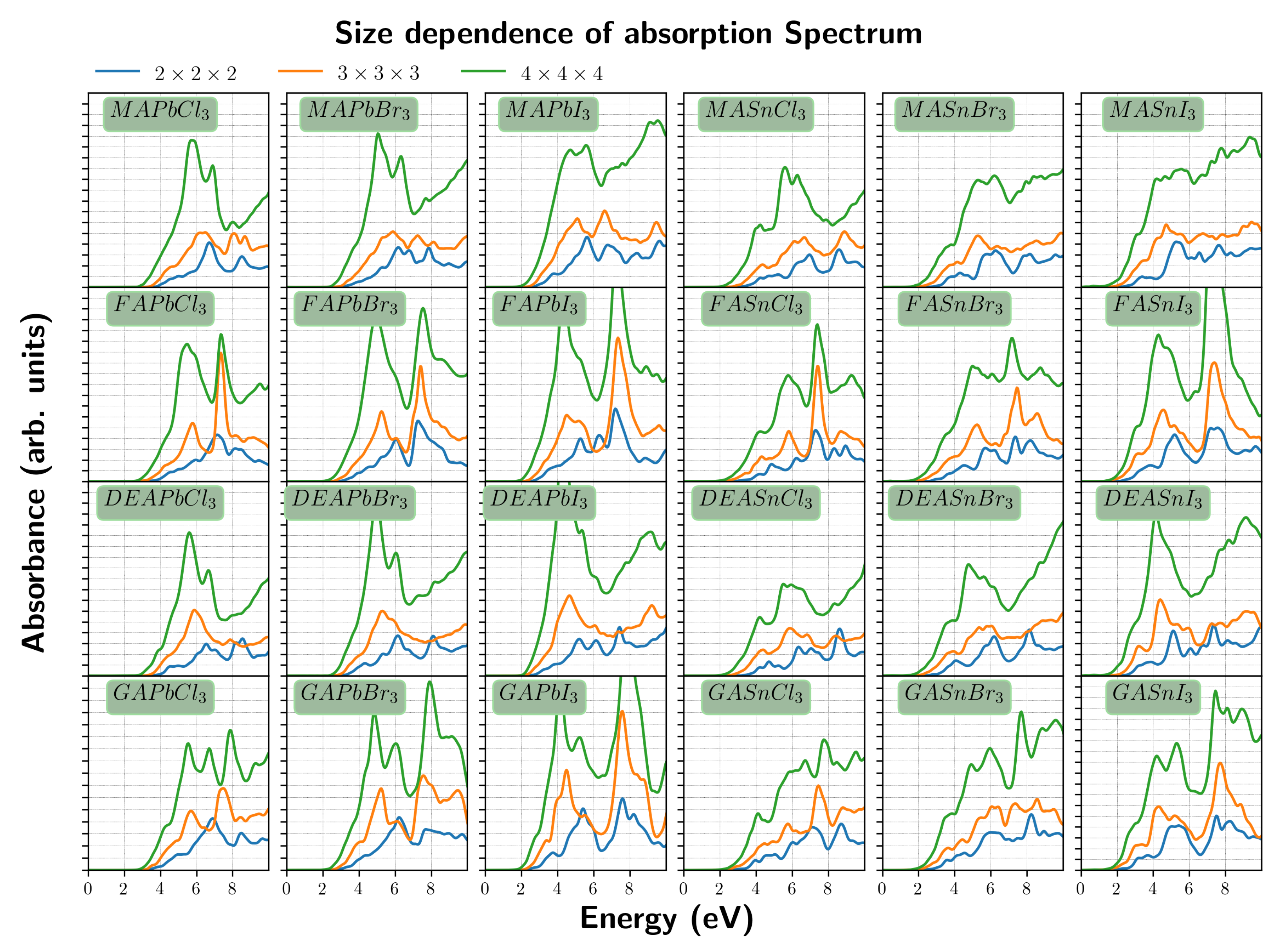
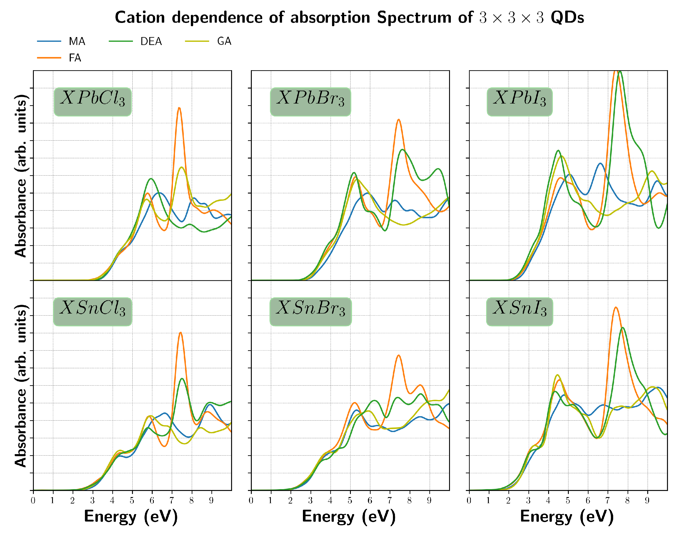
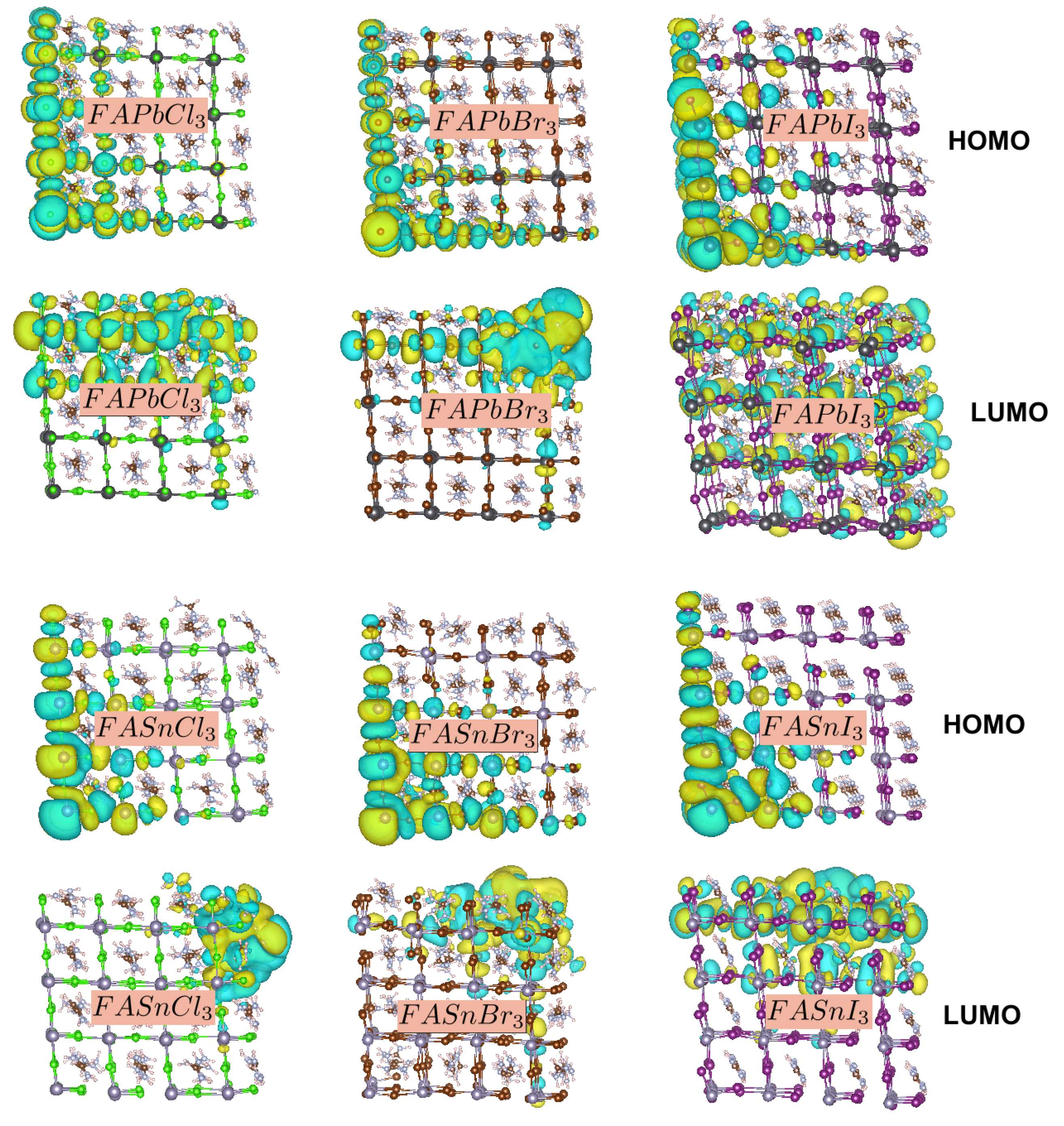
3. Results and Discussion

Before turning our focus on the electronic and optical properties of the nanoparticles considered, it is worth examining their structural properties as revealed by the semi-empirical conformational search and the subsequent DFT optimization. The surface A cations, which in our case are molecular moieties, introduce extra degrees of freedom and an extremely flat potential energy surface, making the convergence of structural relaxation rather difficult. In certain cases, the disorder on the surfaces of the nanoparticle is more pronounced, and it is likely to affect the electronic properties as well. In smaller NPs (e.g., 2 × 2 × 2 ) where the majority of atoms lie on the surface, the atoms of the optimized structures deviate significantly from their ideal positions while larger nanoparticles, despite some deviations from the cubic shape (i.e., α , β , γ angles 90 ° ), tend to retain their clear perovskite structure. In particular, when the A cation is MA, then, for all possible combinations (i.e., B = P b , S n and X = C l , B r , I ), the NP remains cubic. When the A cation is A = F A , D E A , then, for all possible combinations (i.e., B = P b , S n and X = C l , B r , I ), the NPs exhibit a general shape deformation losing their cubic shape and becoming triclinic. The α , β , γ angles exhibit a value ranging from 95° to 98° with the larger values corresponding to larger X anions.
The stability of the NPs can be readily evaluated by examining and comparing their binding energy or their binding energy per atom. Such a procedure would require the calculation of the total energies of the isolated constituent atoms, which can be rather problematic in the GPAW program. For this reason, in order to circumvent this inherent inability of GPAW to adequately treat the single atoms (which is usually manifested as convergence problems), we chose to resort to the binding energy per unit formula (i.e., B E / A B X 3 ) as a stability measure.
B E ( A B X 3 ) k = E t o t k E A B X 3 k , k = n × l × m
This quantity does not require any calculations on atoms and everything runs flawlessly without compromising the accuracy of the results.
The results for all categories of NPs (and sizes 2 × 2 × 2 and 3 × 3 × 3 ) are gathered in Figure 2. A close inspection of the cases where the A cation is either MA or FA or DEA reveals that, overall, the binding energy tends to exhibit a decreasing behavior as the ionic radius of the X anion increases. A striking exception from this trend appears for the case of 2 × 2 × 2 D E A P b I 3 NP. Another tendency that can be identified from this figure is the fact that B = S n NPs seem to systematically exhibit lower binding energies than their B = P b counterparts. Once again, an exception appears for the cases of 2 × 2 × 2 F A P b C l 3 and F A P b I 3 , which appear to have lower binding energies than the corresponding F A S n C l 3 and F A S n I 3 . The deviations from the general trends observed for some of the 2 × 2 × 2 NPs may be attributed to their very small size which makes them prone to large structural distortions. It should be noted that, out of the 8 B cations of the NP, seven are on the surface and only one resides in the interior experiencing the full environment of the bulk. Similarly, 21 out of the 24 X anions are also on the surface. For these reasons, the trends established by the 3 × 3 × 3 NPs might be considered as more reliable. The A = G A NPs also exhibit a slightly erratic behavior deviating from the observed trends. This might be attributed to the larger size of the GA cation, which, in turn, leads to larger shape distortions of the structures. The results for all categories of NPs (and sizes 2 × 2 × 2 and 3 × 3 × 3 ) are gathered in Figure 2. When the A cation is either MA or FA or DEA, the binding energy decreases as the ionic radius of the X anion increases. At the same time, the B = S n NPs systematically exhibit lower binding energies than their B = P b counterparts. The A = G A NPs seem to deviate slightly from the observed trend. This might be attributed to the larger size of the GA cation, which, in turn, leads to larger shape distortions of the structures.
Before considering the dependence of the gap with respect to the size and the composition of the QDs, it is interesting to examine the effect that the orientation of the molecular moieties might have. Such a task would require a large number of calculations in order to adequately sample the space of possible conformations. As a result, it was considered necessary to adopt a fast method and small QDs. A qualitative picture can be drawn by examining the variation of the HOMO-LUMO gap when the P b C l 3 backbone is constrained, while the positions and orientations of A cation moieties are systematically scanned. For example, the conformational search for the case of the 2 × 2 × 2 F A P b C l 3 nanoparticle, in which the P b C l 3 backbone was constrained by means of a suitable potential, produced a few thousands of candidate geometries, which, when optimized with the GFN2-xTB method, they produced HOMO-LUMO gap values exhibiting a non-negligible dispersion. In particular, the standard deviation was found to be as large as 0.22 eV. Apparently, the orientation of the A cations distorts the geometry of the backbone structure, and this leads to small gap variations. It might be expected that this behavior will be more pronounced for the case of larger A cation moieties.
Keeping in mind the last findings, we can proceed to examine the electronic properties of the considered nanoparticles. As already mentioned, all of the best structures from the crest calculation were optimized at a PBE/dzp level of theory, and their electronic structure is analyzed with the help of Projected Density of States diagrams (PDOS). In this way, the single particle gaps and the nature of band edges are revealed. At this point, it should be noted that the adopted functional is a standard GGA one, which suffers from the well known and well documented HOMO-LUMO gap underestimation problem. In the specific type of nanoparticle, it has been shown that the PBE values can be underestimated by as much as 1.5 eV compared to the more accurate and reliable hybrid PBE0 ones [42]. The produced PDOS diagrams for 3 × 3 × 3 NPs are presented in Figure 3 in a 4 × 6 array with each line corresponding to a different type of A cation and each column to a different backbone structure. For the case of methylamonium (line 1), it is clear that, for B = P b , the DOS diagrams show a clean gap with well defined band edges, while, for B = S n containing NPs, surface states seem to emerge. These states are closely related to the larger distortions observed in the B = S n NPs, which, in turn, might be connected with the smaller stability of the specific NPs (see Figure 2). The width of the gap closes as one moves from left to right (the actual values are gathered in Table 1). The states around the HOMO exhibit a large contribution from the anion X regardless of its type ( X = C l , B r , I ). This is consistently true for all types of nanoparticles. Similarly, the states around LUMO appear to come mainly from the anion B regardless of its type ( B = P b , S n ). Even the surface states appearing near the conduction-band-minimum (CBM) exhibit the same parentage.
For the case of formamidinium (FA) containing NPs, presented in line 2 of Figure 3, it can be seen that, even for the B = P b ( X = C l , I ), there are gap states that appear close to the band edges. This happens despite the fact that the specific naoparticles exhibit an enhanced stability (see Figure 2). This can be understood by closely examining the parentage of these states, which appears to be tightly connected with the FA moieties. This behavior is unique since, in all other cases, the states around LUMO are mainly from the B cation with the A cation contributions quite high in the conduction band. As a result, it could be claimed that, for the case of FA, the orientational disorder can enhance the role of FA virtual orbitals in the area around the CBM.
On the other hand, the orientational disorder of the DEA and GA moieties seems to have a smaller effect on the electronic structure of the corresponding nanoparticles. All B = P b structures exhibit a clean gap while gap states are more likely to emerge in B = S n structures. This is a general finding which applies regardless of the A cation.
As already described, the optical properties of the nanoparticles were calculated by suitably perturbing the ground state of the system and letting it evolve in time. In this way, the absorption spectrum is obtained by a Fourier transformation of the recorded dipole moments. The specific procedure does not calculate the discrete spectrum of excited states, but it rather produces the whole spectrum at once. The calculated spectra for the 2 × 2 × 2 and 3 × 3 × 3 dots are presented in Figure 4. These plots reveal the dependence of the absorption properties on the type of the X anion. As can be clearly seen, the ordering is the same for all materials considered. Regardless of A and B cations, X = I NPs always exhibit the smaller optical gap while X = C l the larger. Interestingly, the existence of gap states discussed in Figure 3 does not seem to have a significant impact on the energetic ordering of the spectra (perhaps, there would be larger shifts if the gap states were absent). For example, the presence of the isolated gap state in F A P b C l 3 does not change the ordering with respect to F A P b B r 3 (which has a clean gap).
The effect of the nanoparticles’ size is captured in Figure 5 where the spectra of 2 × 2 × 2 , 3 × 3 × 3 and 4 × 4 × 4 QDs are plotted together. In most of the cases, the blue-shift of the absorption thresholds is evident, while, at the same time, the evolution of the spectrum’s characteristics with size is also evident. If the attention is turned in the first couple of peaks, one can see that, as the size increases, the spectrum characteristics become clearer.
In order to have a complete picture of the calculated optical properties, it is mandatory to examine the dependence of the produced absorption spectra on the type of the A cation. For this purpose, the corresponding plots of the 3 × 3 × 3 nanoparticles are plotted against each other in Figure 6. Interestingly, the absorption thresholds are only marginally affected by the type of A cation. Despite the different size of the A moieties and the subsequent changes to the backbone structure, the differences in the electronic structure (presented in Figure 3) and the existence of the orientational disorder, the absorption thresholds appear to be quite insensitive. The first clearly noticeable differences appear in an energy range ∼2 eV above the absorption threshold.
The frontier orbitals (i.e., HOMO and LUMO) which play a significant role in the determination of the optical gap, systematically exhibit patterns similar to the ones presented in Figure 7. At least for this type of stoichiometric NPs which include facets consisting of truncated B X 6 ocatehedra, the HOMO orbitals appear to be localized on these surfaces. In the same time, the LUMO orbitals appear to be more or less, distributed to the opposite side of the cubic structure. In other words, the frontier orbitals are not well confined in the interior of the NP as is customary in other types of semiconductor QDs. This might be suggestive that their properties may be suitably tailored by surface modification or passivation. Although Figure 7 includes only the orbitals of the F A B X 3 NPs, the trends are similar for all other moieties.

4. Conclusions

In conclusion, the structural, electronic, and optical properties of a wide range of perovskite ( A B X 3 ) nanoparticles (NPs) have been explored with a computational combinatory study, revealing their dependence on their composition and size. The effect of parameters like A cation type, B cation type, X anion type, and size have been systematically examined and presented. It has been found that the orientational disorder of the A cations can affect the electronic properties of the NPs by introducing gap states, while, at the same time, the band gap values may exhibit a non negligible dispersion with a standard deviation as large as 0.2 eV. However, the optical properties as determined by the absorption thresholds appear to be quite insensitive to the presence of gap states obeying clear trends which depend only on the size of the NPs and the type of the X anion. Interestingly, the optical properties are only marginally affected by the type of the A cations.

Author Contributions

C.S.G. has performed the main bulk of the calculations. C.S.G. and I.G. have written a large part of the original draft. S.B., Z.Z. and D.B.H. have equally contributed to the discussion and the interpretation of the results and the preparation of the final manuscript. All authors have read and agreed to the published version of the manuscript.

Funding

This work was financially supported by the Horizon—2020 research and innovation program of the European Union (Grant No. 952335, NanoQIQO project).

Institutional Review Board Statement

Not applicable.

Informed Consent Statement

Not applicable.

Data Availability Statement

The data that support the findings of this study are available from the corresponding author upon reasonable request.

Conflicts of Interest

The authors declare no conflict of interest.

References

  1. Pena, M.A.; Fierro, J.L.G. Chemical structure and performance of perovskite oxides. Chem. Rev. 2001, 101, 1981. [Google Scholar] [CrossRef]
  2. Chen, Q.; De Marco, N.; Yang, Y.M.; Song, T.B.; Chen, C.C.; Zhao, H.; Hong, Z.; Zhou, H.; Yang, Y. Under the spotlight: The organic–inorganic hybrid halide perovskite for optoelectronic applications. Nano Today 2015, 10, 355–396. [Google Scholar] [CrossRef] [Green Version]
  3. Hoefler, S.F.; Trimmel, G.; Rath, T. Progress on lead-free metal halide perovskites for photovoltaic applications: A review. Monatsh. Chem. 2017, 148, 795. [Google Scholar] [CrossRef] [Green Version]
  4. Román-Vázquez, M.; Vidyasagar, C.; Muũnoz Flores, B.M.; Jiménez-Pérez, V.M. Recent advances on synthesis and applications of lead- and tin-free perovskites. J. Alloys Compd. 2020, 835, 155112. [Google Scholar] [CrossRef]
  5. Yang, L.; Barrows, A.T.; Lidzey, D.G.; Wang, T. Recent progress and challenges of organometal halide perovskite solar cells. Rep. Prog. Phys. 2016, 79, 026501. [Google Scholar] [CrossRef]
  6. Yang, G.L.; Zhong, H.Z. Organometal halide perovskite quantum dots: Synthesis, optical properties, and display applications. Chin. Chem. Lett. 2016, 27, 1124. [Google Scholar] [CrossRef]
  7. Johnston, M.B.; Herz, L.M. Hybrid perovskites for photovoltaics: Change-Carrier recombination, diffusion, and radiative efficiencies. Acc. Chem. Res. 2016, 49, 146. [Google Scholar] [CrossRef] [Green Version]
  8. Brittman, S.; Adhyaksa, G.W.P.; Garnett, E.C. The expanding world of hybrid perovskites: Materials properties and emerging applications. MRS Commun. 2015, 5, 7. [Google Scholar] [CrossRef] [PubMed] [Green Version]
  9. Frost, J.M.; Butler, K.T.; Brivio, F.; Hendon, C.H.; van Schilfgaarde, M.; Walsh, A. Atomistic origins of high-performance in hybrid halide perovskite solar cells. Nano Lett. 2014, 14, 2584. [Google Scholar] [CrossRef] [PubMed] [Green Version]
  10. Filippetti, A.; Mattoni, A. Hybrid perovskites for photovoltaics: Insights from first principles. Phys. Rev. B 2014, 89, 125203. [Google Scholar] [CrossRef]
  11. Albero, J.; Asiri, A.M.; Garcia, H. Influence of the composition of hybrid perovskites on their performance in solar cells. J. Mater. Chem. 2016, 4, 4353. [Google Scholar] [CrossRef] [Green Version]
  12. Zhao, Y.; Zhu, K. Organic-inorganic hybrid lead halide perovskites for optoelectronic and electronic applications. Chem. Soc. Rev. 2016, 45, 655. [Google Scholar] [CrossRef]
  13. Zhou, Y.; Yang, M.; Game, O.S.; Wu, W.; Kwun, J.; Strauss, M.A.; Yan, Y.; Huang, J.; Zhu, K.; Padture, N.P. Manipulating crystallization of organolead mixed-halide thin films in antisolvent baths for wide-bandgap perovskite solar cells. ACS Appl. Mater. Interfaces 2016, 8, 22322237. [Google Scholar] [CrossRef]
  14. Quarti, C.; Mosconi, E.; Ball, J.M.; DInnocenzo, V.; Tao, C.; Pathak, S.; Snaith, H.J.; Petrozza, A.; De Angelis, F. Structural and optical properties of methylammonium lead iodide across the tetragonal to cubic phase transition: Implications for perovskite solar cells. Energy Environ. Sci. 2016, 9, 155. [Google Scholar] [CrossRef]
  15. Koliogiorgos, A.; Baskoutas, S.; Galanakis, I. Electronic and gap properties of lead-free perfect and mixed hybrid halide perovskites: An ab-initio study. Comput. Mater. Sci. 2017, 138, 92. [Google Scholar] [CrossRef] [Green Version]
  16. Kovalenko, M.V.; Protesescu, L.; Bodnarchuk, M.I. Properties and potential optoelectronic applications of lead halide perovskite nanocrystals. Science 2017, 358, 745750. [Google Scholar] [CrossRef] [PubMed] [Green Version]
  17. Hwang, J.; Rao, R.R.; Giordano, L.; Katayama, Y.; Yu, Y.; Shao-Horn, Y. Perovskites in catalysis and electrocatalysis. Science 2017, 358, 751756. [Google Scholar] [CrossRef] [Green Version]
  18. Green, M.A. Silicon solar cells: Evolution, high-efficiency design and efficiency enhancements. Semicond. Sci. Technol. 1993, 8, 1. [Google Scholar] [CrossRef]
  19. Grätzel, M. The light and shade of perovskite solar cells. Nat. Mater. 2014, 13, 838. [Google Scholar] [CrossRef] [PubMed]
  20. Correa-Baena, J.P.; Saliba, M.; Buonassisi, T.; Grätzel, M.; Abate, A.; Tress, W.; Hagfeldt, A. Promises and challenges of perovskite solar cells. Science 2017, 358, 739744. [Google Scholar] [CrossRef] [Green Version]
  21. Ono, L.K.; Qi, Y.; Liu, S. Progress toward Stable Lead Halide Perovskite Solar Cells. Joule 2018, 2, 1961. [Google Scholar] [CrossRef] [Green Version]
  22. Sahare, S.; Ghoderao, P.; Khan, S.B.; Chan, Y.; Lee, S.L. Recent progress in hybrid perovskite solar cells through scanning tunneling microscopy and spectroscopy. Nanoscale 2020, 12, 15970. [Google Scholar] [CrossRef]
  23. Xie, H.; Yin, X.; Guo, Y.; Liu, J.; Que, W.; Wang, G. Recent Progress of Flexible Perovskite Solar Cells. Phys. St. Solidi RRL 2019, 13, 1800566. [Google Scholar] [CrossRef]
  24. Jošt, M.; Kegelmann, L.; Korte, L.; Albrecht, S. Monolithic Perovskite Tandem Solar Cells: A Review of the Present Status and Advanced Characterization Methods Toward 30% Efficiency. Adv. Energy Mater. 2020, 10, 1904102. [Google Scholar] [CrossRef]
  25. Daboczi, M.; Kim, J.; Lee, J.; Kang, H.; Hamilton, I.; Lin, C.T.; Dimitrov, S.D.; McLachlan, M.A.; Lee, K.; Durrant, J.R.; et al. Towards Efficient Integrated Perovskite/Organic Bulk Heterojunction Solar Cells: Interfacial Energetic Requirement to Reduce Charge Carrier Recombination Losses. Adv. Funct. Mater. 2020, 30, 2001482. [Google Scholar] [CrossRef]
  26. Asghar, M.; Zhang, J.; Wang, H.; Lunda, P.D. Device stability of perovskite solar cells-A review. Renew. Sust. Energ. Rev. 2017, 77, 131. [Google Scholar] [CrossRef] [Green Version]
  27. Saliba, M.; Correa-Baena, J.P.; Grätzel, M.; Hagfeldt, A.; Abate, A. Perovskite Solar Cells: From the Atomic Level to Film Quality and Device Performance. Angew. Chem. Int. Ed. 2018, 57, 2554. [Google Scholar] [CrossRef] [PubMed]
  28. Shekhirev, M.; Goza, J.; Teeter, J.D.; Lipatov, A.; Sinitskii, A. Synthesis of Cesium Lead Halide Perovskite Quantum Dots. J. Chem. Educ. 2017, 94, 1150. [Google Scholar] [CrossRef]
  29. Hou, J.; Cao, S.; Wu, Y.; Gao, Z.; Liang, F.; Sun, Y.; Lin, Z.; Sun, L. Inorganic Colloidal Perovskite Quantum Dots for Robust Solar CO2 Reduction. Chem.-Eur. J. 2017, 23, 9481. [Google Scholar] [CrossRef]
  30. Bohn, B.J.; Tong, Y.; Gramlich, M.; Lai, M.L.; Döblinger, M.; Wang, K.; Hoye, R.L.Z.; Muüller-Buschbaum, P.; Stranks, S.D.; Urban, A.S.; et al. Boosting Tunable Blue Luminescence of Halide Perovskite Nanoplatelets through Postsynthetic Surface Trap Repair. Nano Lett. 2018, 18, 5231. [Google Scholar] [CrossRef] [Green Version]
  31. Yang, D.; Zou, Y.; Li, P.; Liu, Q.; Wu, L.; Hu, H.; Xu, Y.; Sun, B.; Zhang, Q.; Lee, S.T. Large-scale synthesis of ultrathin cesium lead bromide perovskite nanoplates with precisely tunable dimensions and their application in blue light-emitting diodes. Nano Energy 2018, 47, 235. [Google Scholar] [CrossRef]
  32. Tong, Y.; Fu, M.; Bladt, E.; Huang, H.; Richter, A.F.; Wang, K.; Muller-Buschbaum, P.; Bals, S.; Tamarat, P.; Lounis, B.; et al. Chemical Cutting of Perovskite Nanowires into Single-Photon Emissive Low-Aspect-Ratio CsPbX3 (X = Cl, Br, I) Nanorods. Angew. Chem. Int. Ed. 2018, 57, 16094. [Google Scholar] [CrossRef] [PubMed]
  33. Bai, Z.; Zhong, H. Halide perovskite quantum dots: Potential candidates for display technology. Sci. Bull. 2015, 60, 1622. [Google Scholar] [CrossRef] [Green Version]
  34. Zhang, F.; Zhong, H.; Chen, C.; Wu, X.g.; Hu, X.; Huang, H.; Han, J.; Zou, B.; Dong, Y. Brightly Luminescent and Color-Tunable Colloidal CH3NH3PbX3 (X = Br, I, Cl) Quantum Dots: Potential Alternatives for Display Technology. ACS Nano 2015, 9, 4533. [Google Scholar] [CrossRef] [PubMed]
  35. Tanaka, K.; Takahashi, T.; Ban, T.; Kondo, T.; Uchida, K.; Miura, N. Comparative study on the excitons in lead-halide-based perovskite-type crystals CH3NH3PbBr3 CH3NH3PbI3. Solid State Commun. 2003, 127, 619. [Google Scholar] [CrossRef]
  36. Mali, S.S.; Shim, C.S.; Hong, C.K. Highly stable and efficient solid-state solar cells based on methylammonium lead bromide (CH3NH3PbBr3) perovskite quantum dots. Npg Asia Mater. 2015, 7, 208. [Google Scholar] [CrossRef] [Green Version]
  37. Castañeda, J.A.; Nagamine, G.; Yassitepe, E.; Bonato, L.G.; Voznyy, O.; Hoogland, S.; Nogueira, A.F.; Sargent, E.H.; Cruz, C.H.B.; Padilha, L.A. Efficient Biexciton Interaction in Perovskite Quantum Dots Under Weak and Strong Confinement. ACS Nano 2016, 10, 8603. [Google Scholar] [CrossRef]
  38. Peng, L.; Geng, J.; Ai, L.; Zhang, Y.; Xie, R.; Yang, W. Room temperature synthesis of ultra-small, near-unity single-sized lead halide perovskite quantum dots with wide color emission tunability, high color purity and high brightness. Nanotechnology 2016, 27, 335604. [Google Scholar] [CrossRef]
  39. Chen, X.; Peng, L.; Huang, K.; Shi, Z.; Xie, R.; Yang, W. Non-injection gram-scale synthesis of cesium lead halide perovskite quantum dots with controllable size and composition. Nano Res. 2016, 9, 1994. [Google Scholar] [CrossRef]
  40. Buin, A.; Comin, R.; Ip, A.H.; Sargent, E.H. Perovskite Quantum Dots Modeled Using ab Initio and Replica Exchange Molecular Dynamics. J. Phys. Chem. C 2015, 119, 13965. [Google Scholar] [CrossRef]
  41. He, J.; Vasenko, A.S.; Long, R.; Prezhdo, O.V. Halide Composition Controls Electron–Hole Recombination in Cesium–Lead Halide Perovskite Quantum Dots: A Time Domain Ab Initio Study. J. Phys. Chem. Lett. 2018, 9, 1872. [Google Scholar] [CrossRef]
  42. Koliogiorgos, A.; Garoufalis, C.S.; Galanakis, I.; Baskoutas, S. Electronic and optical properties of ultrasmall ABX3 (A = Cs, CH3NH3, B = Ge, Pb, Sn, Ca, Sr, X = Cl, Br, I) perovskite quantum dots. ACS Omega 2018, 3, 18917. [Google Scholar] [CrossRef] [PubMed]
  43. Grimme, S.; Bannwarth, C.; Shushkov, P. A Robust and Accurate Tight-Binding Quantum Chemical Method for Structures, Vibrational Frequencies, and Noncovalent Interactions of Large Molecular Systems Parametrized for All spd-Block Elements (Z = 1–86). J. Chem. Theory Comput. 2017, 13, 1989–2009. [Google Scholar] [CrossRef] [PubMed]
  44. Bannwarth, C.; Ehlert, S.; Grimme, S. GFN2-xTB—An Accurate and Broadly Parametrized Self-Consistent Tight-Binding Quantum Chemical Method with Multipole Electrostatics and Density-Dependent Dispersion Contributions. J. Chem. Theory Comput. 2019, 15, 1652–1671. [Google Scholar] [CrossRef] [Green Version]
  45. Pracht, P.; Bohle, F.; Grimme, S. Automated exploration of the low-energy chemical space with fast quantum chemical methods. Phys. Chem. Chem. Phys. 2020, 22, 7169–7192. [Google Scholar] [CrossRef] [PubMed]
  46. Grimme, S. Exploration of Chemical Compound, Conformer, and Reaction Space with Meta-Dynamics Simulations Based on Tight-Binding Quantum Chemical Calculations. J. Chem. Theory Comput. 2019, 15, 2847–2862. [Google Scholar] [CrossRef]
  47. Mortensen, J.J.; Hansen, L.B.; Jacobsen, K.W. Real-space grid implementation of the projector augmented wave method. Phys. Rev. B 2005, 71, 035109. [Google Scholar] [CrossRef] [Green Version]
  48. Perdew, J.P.; Burke, K.; Ernzerhof, M. Generalized gradient approximation made simple. Phys. Rev. Lett. 1996, 77, 3865–3868. [Google Scholar] [CrossRef] [Green Version]
  49. Larsen, A.H.; Mortensen, J.J.; Blomqvist, J.; Castelli, I.E.; Christensen, R.; Dułak, M.; Friis, J.; Groves, M.N.; Hammer, B.; Hargus, C.; et al. The atomic simulation environment—A Python library for working with atoms. J. Phys. Condens. Matter 2017, 29, 273002. [Google Scholar] [CrossRef] [PubMed] [Green Version]
  50. Walter, M.; Häkkinen, H.; Lehtovaara, L.; Puska, M.; Enkovaara, J.; Rostgaard, C.; Mortensen, J.J. Time-dependent density-functional theory in the projector augmented-wave method. J. Chem. Phys. 2008, 128, 244101. [Google Scholar] [CrossRef] [Green Version]
  51. Kuisma, M.; Sakko, A.; Rossi, T.P.; Larsen, A.H.; Enkovaara, J.; Lehtovaara, L.; Rantala, T.T. Localized surface plasmon resonance in silver nanoparticles: Atomistic first-principles time-dependent density-functional theory calculations. Phys. Rev. B 2015, 91, 115431. [Google Scholar] [CrossRef] [Green Version]
Figure 1. Neutral 3 × 3 × 3 quantum dots. In (a), the main building block is the B X 6 octahedron. If all interstitial sites are occupied by A cations, then the resulting structure exhibits an excess of positive charge ( + 10 for the specific dot). Neutrality may be achieved by randomly removing the appropriate number of A cations (for example, random sites are indicated by the large red spheres). In (b), the main building block is the A B X 3 unit. As a result, the resulting nanoparticles are always neutral, but three out of six facets are terminated by truncated octahedra.
Electronicmat 02 00026 g001
Figure 2. The binding energy per unit formula for all 2 × 2 × 2 and 3 × 3 × 3 nanoparticles considered.
Electronicmat 02 00026 g002
Figure 3. The projected density of states of all 3 × 3 × 3 nanoparticles considered.
Electronicmat 02 00026 g003
Figure 4. Dependence of the absorption spectra on X anion type for NPs with sizes 2 × 2 × 2 and 3 × 3 × 3 .
Electronicmat 02 00026 g004
Figure 5. Dependence of the absorption spectra on the size of the nanoparticle (i.e., 2 × 2 × 2 , 3 × 3 × 3 and 4 × 4 × 4 QDs).
Electronicmat 02 00026 g005
Figure 6. Dependence of the absorption spectra on the A cation type.
Electronicmat 02 00026 g006
Figure 7. Plots of the HOMO and LUMO molecular orbitals for the case of 3 × 3 × 3 , F A B X 3 nanoparticles. In all cuboids, the atom residing in the bottom right corner corresponds to the X anion, and the remaining color corresponds to the B cation.
Electronicmat 02 00026 g007
Table 1. HOMO-LUMO gap in eV for all nanoparticles under study.
A = MA
PbSn
ClBrIClBrI
2 × 2 × 2 3.552.972.502.782.101.84
3 × 3 × 3 3.342.842.281.801.621.25
4 × 4 × 4 2.872.381.481.481.160.45
A = FA
PbSn
ClBrIClBrI
2 × 2 × 2 2.361.811.940.971.360.86
3 × 3 × 3 1.822.491.871.011.220.83
4 × 4 × 4 2.551.881.530.650.730.90
A = DEA
PbSn
ClBrIClBrI
2 × 2 × 2 3.502.952.462.822.012.16
3 × 3 × 3 3.292.651.651.801.401.65
4 × 4 × 4 2.902.501.501.690.850.55
A = GA
PbSn
ClBrIClBrI
2 × 2 × 2 3.212.902.292.332.161.67
3 × 3 × 3 2.712.351.791.401.220.84
4 × 4 × 4 2.622.001.420.730.780.76
Publisher’s Note: MDPI stays neutral with regard to jurisdictional claims in published maps and institutional affiliations.

