Article

Degree of Polarization of Cathodoluminescence from a GaAs Facet in the Vicinity of an SiN Stripe

by
Daniel T. Cassidy
1,*,
Jean-Pierre Landesman
2,
Merwan Mokhtari
3,
Philippe Pagnod-Rossiaux
3,
Marc Fouchier
4 and
Christian Monachon
4
1
Department of Engineering Physics, McMaster University, Hamilton, ON L8S 4L7, Canada
2
Institut FOTON–UMR 6082, Université de Rennes, INSA Rennes, CNRS, 35000 Rennes, France
3
3SP Technologies, Route de Villejust, CEDEX, 91625 Nozay, France
4
Attolight AG, 1015 Lausanne, Switzerland
*
Author to whom correspondence should be addressed.
Optics 2023, 4(2), 272-287; https://doi.org/10.3390/opt4020019
Submission received: 9 February 2023 / Revised: 5 March 2023 / Accepted: 14 March 2023 / Published: 23 March 2023

Abstract

:
Measurements of the cathodoluminescence (CL) and the degree of polarization (DOP) of (CL) from the facet of a GaAs substrate and in the vicinity of a SiN stripe are reported and analyzed. The deformation induced by the SiN stripe is estimated by fitting the measured DOP to 3D finite element method (FEM) simulations. The deformation is found to be more complex than an initial condition of biaxial stress in the SiN. A ratio of fit coefficients suggests that the dependence of DOP on strain is described by equations presented in Appl. Opt. 59, 5506–5520 (2020). These equations give a DOP that is either proportional to a weighted difference of the principal components of strain in the measurement plane, or proportional to the shear strain in the measurement plane, depending on the chosen orientation of the measurement axes.

1. Introduction

Strong interest exists for the characterization of devices and materials, with new approaches to extract material and device parameters [1]. Our interest lies in estimation of strain in III–V materials and devices by analysis of the degree of polarization (DOP) of luminescence, for which engagement is strong and current [2,3,4,5,6,7,8,9,10]. The DOP of luminescence from InP and GaAs, and related compounds, is a sensitive function of the strain in these III–V materials [11,12,13].
In this paper, we analyze cathodoluminescence (CL) [14,15] from the facet of a GaAs substrate and in the vicinity of an SiN stripe, which was deposited on the top surface of the GaAs substrate. Most previous DOP work has analyzed electroluminescence (EL) or photoluminescence (PL).
The ever-increasing level of the device integration of semiconductor materials into complex micrometer-scale structures, for instance, in photonic integrated circuits (PICs) as well as in solid-state lasers, makes the availability of a technique capable of revealing small strains at micrometer scales highly desirable. A DOP measurement based on cathodoluminescence is interesting in this context because CL has a probe diameter that is not determined by optical diffraction, which enables DOP measurements with sub-micrometer spatial resolution.
Ultimately, we fit, using a least squares approach, 3D finite element method (FEM) simulations of the DOP of luminescence of a strained SiN-stripe-on-GaAs system to the measured DOP of the CL. To obtain the parameters needed in the fits of the FEM simulations to the data and to obtain insights into the CL, we investigated aspects of the measured CL in the vicinity of the edge of the sample.
The results from fits of the 3D FEM simulations of the DOP of luminescence to the measured data are consistent with the theoretical work reported in [16]. This theoretical work, which is based on Bahder’s analytic expressions for the strain dependence of the conduction and valence band dispersions [17,18], gives an expression for the strain dependence of the DOP that is more complicated than the expression that previously was thought to hold [13]. A confirmation of the applicability of [16] for the strain dependence of the DOP of luminescence from GaAs has not, to our knowledge, been reported.
The importance of the work lies in the approach of using fits to luminescence and of using accurate expressions for the strain dependence of the DOP of luminescence to determine parameters that are important for understanding device performance. Strain has long been understood to affect not only the reliability but also the operation of devices [19]. With accurate estimations of strain through fits to DOP measurements, it should be possible to provide input for accurate simulations for device design and for the understanding of operation.
The DOP of luminescence is measured as
D O P n ^ = L h ^ L v ^ L h ^ + L v ^
where L h ^ and L v ^ are the detected luminescences that are emitted along the normal n ^ to the surface under study and polarized along two orthogonal directions, h ^ and v ^ , where h stands for horizontal and v stands for vertical [20]. L h ^ + L v ^ is the total detected luminescence, i.e., the luminescence yield.
A second independent measurement of the DOP of luminescence, which we call ROP for rotated degree of polarization, is made for h ^ and v ^ rotated by 45 deg about the external normal to the surface n ^ . This defines the measured ROP of luminescence as
R O P n ^ = L h ^ L v ^ L h ^ + L v ^
where L h ^ and L v ^ are the detected luminescences that are emitted along the normal n ^ to the surface under study and polarized along the h ^ and v ^ directions [11,21,22]. The luminescence yield as determined from R O P n ^ or from D O P n ^ should be the same.

1.1. DOP as a Function of Strain

The strain dependence of the degree of polarization (DOP) of luminescence from GaAs or InP can be written as a function of the shear deformation potentials b or d if one assumes a value for the ratio d / b , i.e., d = ξ b . To reduce the number of variables in the equations that follow, numerical values are substituted for the remaining physical constants that describe the band structure [23] and for the three independent elastic stiffness constants ([24], Chapter VIII) of the GaAs substrate.
For the luminescence from the normal to a GaAs { 110 } facet and assuming that d = ξ b , the predicted relationships between the degree of polarization (DOP), the rotated degree of polarization (ROP), and strain ([16], Section 3.D.4) are
D O P 110 = | K e | 0.3659 ξ + 1.0218 e 1 + 0.1140 ξ 9.5356 e 3
and
R O P 110 = | K e | 0.5867 ξ ( 2 e 5 )
with the calibration constant K e = 3 b / ( 4 k B T ) ([16], Equation (26)), ([25], Equation (16)), where k B is the Boltzman constant and T is the absolute temperature, and where the normal n ^ to the facet is a 110 direction, h ^ and e 1 are in the plane of the facet and along a 1 1 ¯ 0 direction, and v ^ and e 3 are in the growth or 001 direction. e 5 is a tensor shear strain in the plane of the facet. Note that a Voigt notation is used to reduce the number of subscripts: e 1 = e 11 , e 3 = e 33 , and e 5 = e 13 in terms of components of the strain tensor.
Equations (3) and (4) give the dependence of the degree of the polarization of luminescence on strain as a function of the deformation potential b ( K e is a linear function of b) and the ratio ξ = d / b of the deformation potentials. The deformation potentials are experimentally determined parameters, are different for GaAs and InP, and have uncertainties associated with them [23]. These two equations give the strain dependence in a somewhat general form. Expressed in this form, one can see that D O P 110 depends on a weighted difference of the principal components of strain in the horizontal and vertical directions and that R O P 110 depends on the shear strain, regardless of the value of ξ .
For luminescence from the normal to a GaAs { 110 } facet and assuming the recommended relationship of d = 2.4 b ([23], Table I, p. 5825), the predicted relationships between the degree of polarization (DOP), the rotated degree of polarization (ROP), and strain ([16], Section 3.D.4), are
D O P 110 = | K e | ( 1.252 e 1 0.8132 e 3 )
and
R O P 110 = | K e | 1.408 ( 2 e 5 ) .
Under the simplifying assumption that the material is isotropic, then ([16], Section 4.A.1)
D O P 110 = | K e | ( e 1 e 3 )
and
R O P 110 = | K e | ( 2 e 5 ) .
These expressions permit estimation of the DOP and ROP for a given strain field. These expressions also provide a route to estimate the strain field by fitting DOP and ROP values obtained through the FEM simulations of strain fields to measured degree of polarization data.
In this paper, 3D finite element method (FEM) simulations [26] were fit, using a least squares approach, to measurements of the degree of polarization of cathodoluminescence from a cleaved { 110 } facet of a GaAs substrate in the vicinity of an SiN stripe.
The constants 1.252 , 0.8132 , and 1.408 of Equations (5) and (6) were included in the 3D FEM simulations. Thus, the ratio of the R O P 110 to D O P 110 fit coefficients should equal unity if Equations (3) and (4) are accurate descriptions of the dependence of the DOP and ROP on strain and if d = 2.4 b .

1.2. Least Squares Fits

Least squares fits to the measured DOP data Y D O P ( h , v ) and ROP data Y R O P ( h , v ) were obtained by minimizing reduced chi-square with respect to fitting parameters { a i , b i } . Note that a subscripted b, b i , indicates a fitting parameter and should not be confused with the deformation potential b, which is not subscripted. The meaning of the variable should be clear from context and by the presence of the subscript.
Three-dimensional FEM simulations for the strain field in the vicinity of a SiN stripe on a GaAs substrate were performed to obtain N s `basis functions’ f i ( D O P ) ( h , v ) and f i ( R O P ) ( h , v ) using Equations (5) and (6). These N s basis functions are the DOP and ROP fields obtained from the 3D FEM simulations for the given initial conditions in the SiN stripe or GaAs substrate. The initial conditions are estimates of the state of stress or strain in the materials prior to the attachment of the SiN to the GaAs substrate. The (final) state of stress or strain in the SiN and GaAs is determined with the FEM solver. If the least squares fit of a basis function to the measured data was perfect, then we would conclude that the stress or strain in the SiN was the initial condition that led to the perfectly fitting basis function.
Reduced chi-squares for DOP and ROP fits were defined as
χ D O P 2 = h , v Y D O P ( h , v ) i = 1 N s a i f i ( D O P ) ( h , v ) i = N s + 1 N f a i f i ( h , v ) 2 / ( σ 2 ν D O P )
and
χ R O P 2 = h , v Y R O P ( h , v ) i = 1 N s b i f i ( R O P ) ( h , v ) i = N s + 1 N f b i f i ( h , v ) 2 / ( σ 2 ν R O P )
where h and v are the parameters that give the horizontal and vertical position of the measurement, σ is the rms noise for each data point, ν D O P and ν R O P are the number of degrees of freedom for χ D O P and χ R O P , N f is the number of fit parameters, and f i ( h , v ) are polynomials in h and v that describe the background, which is composed of the offsets, birefringence, and polarization dependence of the optics, and other unavoidable artifacts that are not in the FEM simulations.
The background basis functions were taken as
f N s + 1 ( h , v ) = 1 f N s + 2 ( h , v ) = v f N s + 3 ( h , v ) = h f N s + 4 ( h , v ) = ( v v ¯ ) 2 f N s + 5 ( h , v ) = ( h h ¯ ) 2 f N s + 6 ( h , v ) = ( v v ¯ ) ( h h ¯ )
with v ¯ equal to the average value of v and h ¯ equal to the average value of h.
A total reduced chi-square, χ T , was defined as
χ T 2 = ν D O P χ D O P 2 + ν R O P χ R O P 2 ν D O P + ν R O P
and it was χ T that was minimized with respect to the fit parameters { a i , b i } , subject to the constraint that b i = R a × a i , for i N s where R a was set to a number and was not minimized in the least squares fitting procedure.
If Equations (5) and (6) are correct, and if d / b = 2.4 , then R a = 1 . If R a 1 , then either the equations are incorrect, or d / b 2.4 , or both. The inclusion of R a as a constraint expresses the fact that D O P 110 and R O P 110 should scale together. If the influence that causes the strain distribution is increased by a factor of, e.g., ten, then D O P 110 and R O P 110 should scale by the same factor and the ratio b i / a i should equal R a , for i N s .

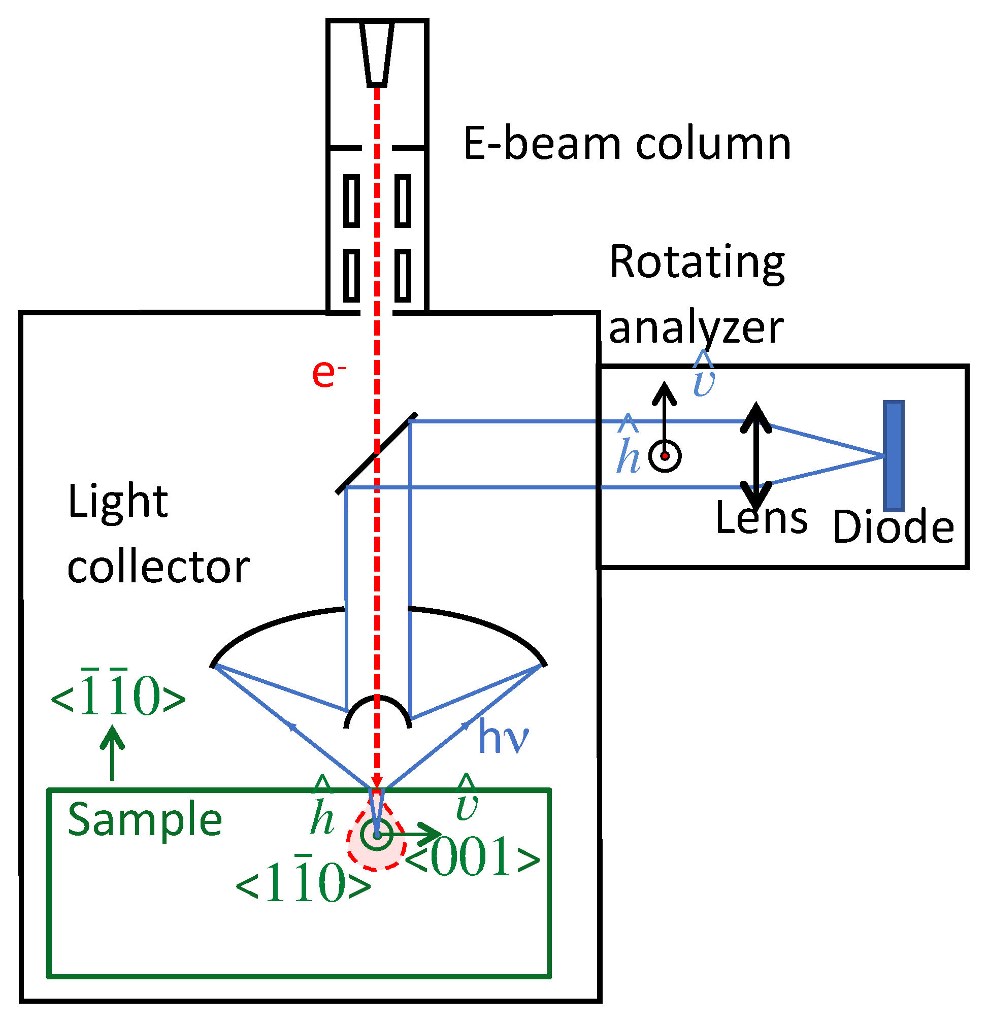
2. Sample and SEM Measurements

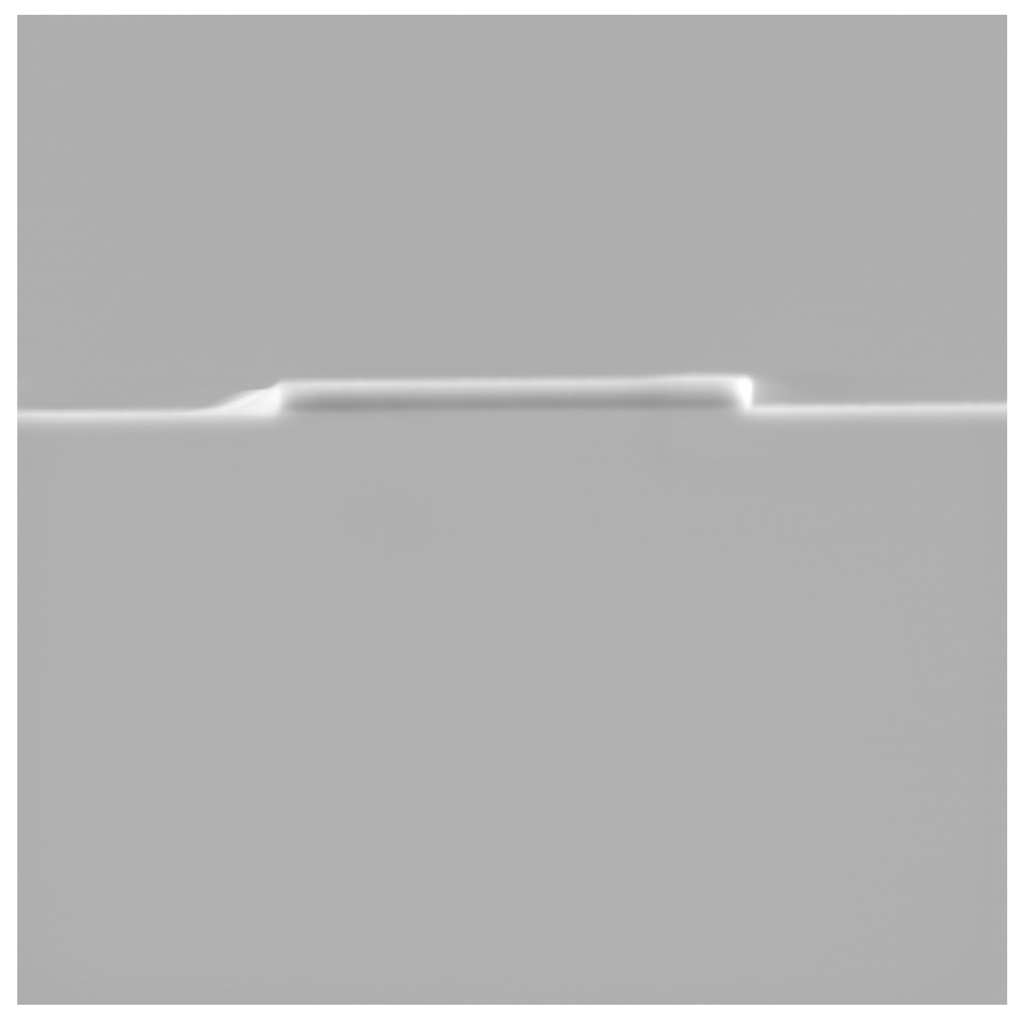
2.1. SiN Stripes on GaAs
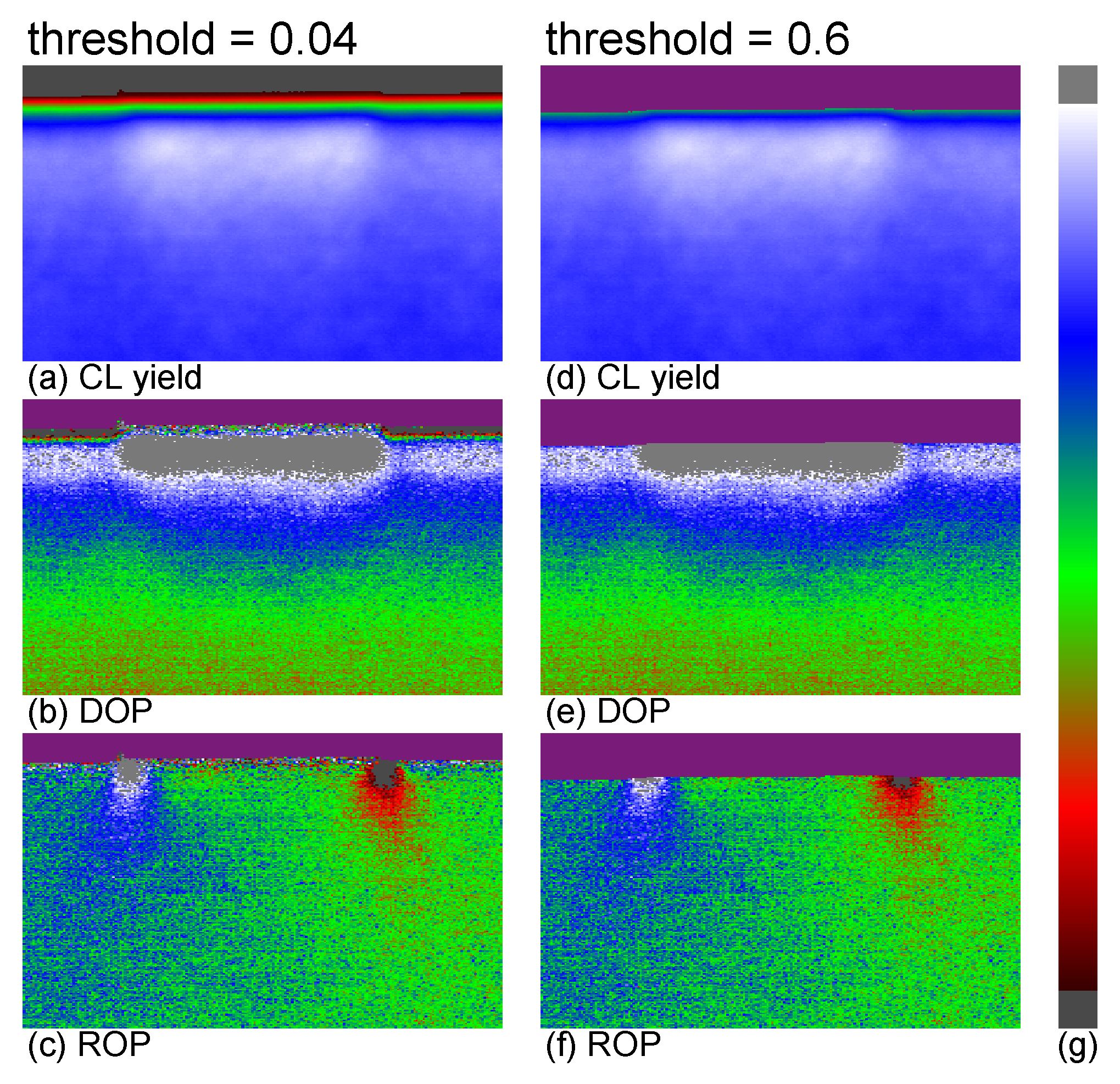
Compressive, 290 nm-thick SiN layers were deposited on ( 100 ) GaAs substrates by a standard PECVD technique, using SiH4, N2, and He as precursors. After deposition, a stress of 220 MPa was measured at the wafer level through the measurement of the wafer bow. Wafers were then processed with standard UV contact lithography to define the stripes of various widths and groupings by the reactive ion etching of the SiN layers and the removal of the photoresist. Bars of 3 mm width in the n ^ direction and of 368 μ m thickness in the v ^ direction were cleaved for scanning electron microscope (SEM) and CL analysis. The backside of the wafer was not polished.

2.2. SEM Data

CL experiments were conducted at room temperature on an Attotlight Allalin spectroscopy platform with a beam current in the 10–15 nA range [27]. During the measurements, a focused electron beam scans the sample while the optical emission is collected and detected by an Si detector, enabling the simultaneous acquisition of secondary electron (SE) and CL intensity images. The e-beam energy was 5 keV, leading to a penetration depth of primary electrons in GaAs of approximately 150 nm. It was found that 5 keV was a good compromise between signal intensity (to improve the signal to noise ratio, which is especially important as DOP is a differential ratiometric technique, and is therefore especially prone to noise), and spatial resolution, as a higher accelerating voltage would result in a larger interaction depth as well as a lower resolution.
The degree of polarization data was obtained by adding a wire grid polarizer before the Si detector as in Ref. [15] but mounted on a motorized holder. Images with the polarizer oriented in the vertical v ^ and horizontal h ^ directions were acquired sequentially to calculate the DOP. Afterwards, images were acquired with the polarizer rotated by ± 45 deg from h ^ to obtain the ROP data. The number of pixels per image was set to 1024 × 1024 and the integration time per pixel to 10 μ s, leading to a time per image of approximately 11 s.
Figure 1 is a schematic diagram of the measurement system and Figure 2 displays a cropped SEM image of a cleaved facet in the vicinity of an SiN stripe.
Panels (a), (b), and (c) of Figure 3 display the measured CL yield, DOP, and ROP using a false color mapping, respectively. The DOP and ROP displays were thresholded at 4 % of the maximum value of the CL yield, i.e., at 0.04 × C L max . This value corresponds to ≈ 5 × the rms value of the bottom fifty rows of the CL yield. Areas for the DOP and ROP that were calculated for the CL yield < 0.04 of the maximum value of the CL yield are displayed in a magenta color. The low threshold allows the estimation of the location of the top of the substrate.
The color bar, (g) of Figure 3, shows the linear, false color mapping that was used. The top and bottom squares of (g) are colors that were used to display off-scale values. The black/red colors at the bottom of the color bar display smaller values of the signal than the blue/white colors at the top of the scale. For signed signals such as the DOP and ROP, a green color at the mid-point of the color bar represents zero. If g is the display gain, then the just off-scale colors represent a DOP or a ROP value of ± 29.16 / g % relative to the midpoint of the color bar. For the data presented in the figures, the DOP display gain g = 10 and the ROP display gain g = 15 , giving just off-scale values of ± 2.92 % and ± 1.94 % , relative to the center of the color bar.
Panels (d), (e), and (f) of Figure 3 display the same data as in (a), (b), and (c), but with the DOP and ROP thresholded at 0.6 of the maximum value of the CL yield. This threshold should remove edge effects, i.e., it should remove artifacts in the calculated DOP and ROP for measurements that are of low CL yield and thus dominated by noise, or for measurements that are too close to the edge of the sample and are thus corrupted by polarized reflections, and is the threshold that was used for the least squares fits of 3D FEM simulations to the DOP and ROP data.
Each panel of Figure 3 displays the same area of 5.46 μ m in the v ^ or vertical direction by 8.92 μ m in the h ^ or horizontal direction. Similarly to Figure 2, the SiN stripe is approximately centered left–right and is near the top. In panels (a) and (d) of Figure 3, which display the CL yield, the cleaved facet of the GaAs substrate shows as blue or white. The top edge of the GaAs substrate lies in the black-red-green bands, which indicate the CL yield increasing (note the colors in the color bar, panel (g)) as the GaAs is approached from above, as is shown later in Figure 4. The SiN sits on top of the gray areas in panels (b) and (e) and in between the blue and red lobes of panels (c) and (f). The effects of the SiN stripe on the CL yield, the DOP, and the ROP are readily apparent in the panels of Figure 3 by comparing the colors at the bottom of each panel to the colors near the top of each panel.
Measurements of the polarized CL were made for four different angles of the polarizers. The polarized CL yield along one axis, P 1 , was made for the polarizer transmission axis along the h ^ direction (i.e., the 1 1 ¯ 0 direction). P 2 was measured for the transmission axis along the v ^ direction (i.e., the 001 direction). P 3 and P 4 were measured for the polarizer transmission axis at ± 45 deg to the h ^ direction.
P 1 , P 2 , P 3 , and P 4 were zero corrected by subtracting the average value of the raw data for 200 full rows of data that were off the sample. These rows are not visible in Figure 2 as these rows were at the top of the file (rows 824–1023) and are not displayed.
With these definitions, using the zero-corrected versions, and using the supplied constants as determined from an unstrained sample,
C L DOP = P 1 + 0.94328 P 2
D O P = P 1 0.94328 P 2 C L DOP
and
C L ROP = P 3 + 1.00385 P 4
R O P = P 3 1.00385 P 4 C L ROP .
Equation (14) is the defining equation for the experimentally determined DOP, Equation (7), with L h ^ = P 1 and L v ^ = 0.94328 P 2 . Equation (16) is the defining equation for the experimentally determined ROP, Equation (8), with L h ^ = P 3 and L v ^ = 1.00385 P 4 .
The constants 0.94328 and 1.00385 account for the polarization-dependent transmission of the measurement system.
The identification of Equations (13) and (15) as the CL yields follows from the measurements of the CL at two orthogonal directions, as pointed out below the defining equations for the experimentally measured DOP and ROP, Equations (7) and (8). C L D O P should equal, within experimental uncertainty, C L R O P .
The field of view was specified as 8.949 μ m, with 1024 × 1024 equally spaced measurements on a horizontal–vertical grid. This gives x s t e p = y s t e p = 8.949 × 10 3 / 1023 = 8.748 nm where the step sizes are the distances between measurements in the horizontal ( h ^ ) or vertical ( v ^ ) directions.
To reduce the size of the files, the cropped P 1 , P 2 , P 3 , and P 4 files were averaged over a rectangle with height of 3 (raw) data points in the vertical direction and a width of 5 (raw) data points in the horizontal direction. This reduced the files sizes to 204 points in the horizontal direction and 208 points in the vertical direction. This gives an h s t e p = 5 × x s t e p = 0.04374 μ m and a v s t e p = 3 × y s t e p = 0.02624 μ m. Note the use of h s t e p and v s t e p to distinguish from x s t e p and y s t e p .

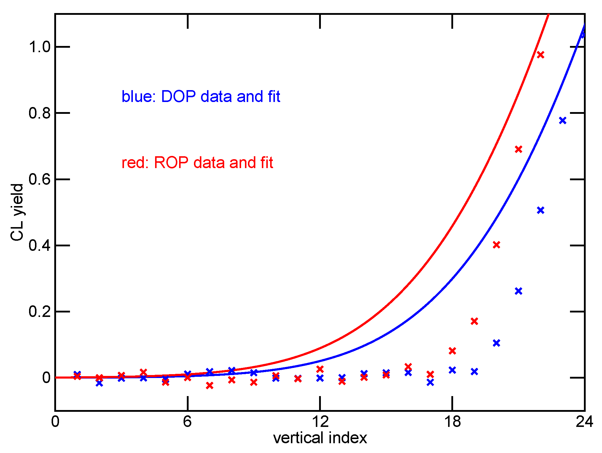
3. Fits to the CL Yield

The CL yields ( C L DOP and C L ROP ) were analyzed to provide values needed in the least squares fitting of FEM simulations of the SiN stripes on GaAs to the measured degree of polarization data.
Complementary error functions as functions of vertical distance v and for a chosen h,
A 2 erfc v e v σ v 2 ,
were fit to the CL yields to determine the best-fit estimates of the locations of the top edges of the samples, v e , and the full-width half-maximum (FWHM) resolutions. For a Gaussian function with scale parameter (i.e., standard deviation) σ v , the FWHM = 2.35482 σ v . The parameter A gives the best-fit value of the CL yield for the substrate away from the top edge of the sample. h specifies which column of vertical data is fit to the complementary error function. h × h s t e p is the horizontal distance from the left-hand edge of the full measurement area.
The complementary error function in Equation (17) is proportional to the area of a Gaussian function over the interval ( v e v , ] and is a function of v e v where v e is a number and gives the location in the vertical direction of the top edge of the sample. If the electron beam of the SEM is Gaussian in the cross-section and if the CL yield is proportional to the fraction of the electron beam that is on-the-sample, then Equation (17) should provide an accurate description of the CL yield.
Equation (17) is particularly useful near the edge of the sample, in cases for which the electron beam is not fully on-the-sample and not fully off-the-sample, i.e., when v v e . For the electron beam fully off-the-sample, v = , erfc ( ) = 0 and there is no CL yield. For v = v e , the electron beam is half on the sample, erfc ( 0 ) = 1 , and the CL yield is A / 2 , which is half the maximum value. If the electron beam is fully on the sample, v = + , erfc ( ) = 2 , and the CL yield is a maximum and equals A.
Table 1 lists values found from fits of a vertical column of CL yield data to Equation (17). h × h s t e p specifies the vertical column by the distance from the left hand edge. The value of χ is the rms value of the residue, where the residue is the difference between the data points and the best fit curve. A is the best fit CL yield far from the location of the top edge v e of the sample. The FWHM = 2.35482 σ v is a measure of the diameter of the CL probe and shows that sub-micrometer resolution is achieved with the CL measurement system.
Figure 4a shows a fit of Equation (17) to the CL yields for h = 102 , where h is a horizontal distance and has units of h s t e p . The top left edge of the sample occurs at the ordered pair ( h = 1 , v e ) , the top right edge occurs at ( h = 204 , v e ) , and the middle of the SiN stripe is roughly ( h = 102 , v e ) .
Note that the horizontal axis of Figure 4 gives the distance in units of v s t e p from the top of the file and along the line h = 102 . The point with vertical index = 20 is 20 rows below the top row of the CL data file, i.e., 20 × v s t e p = 0.5258 μ m below the top of the file.
Figure 4b displays a fit of Equation (17) to the CL yields for h = 18 , a region that is well away from the SiN stripe. By the comparison of Figure 4a to b, one can see that the fits differ for values near the vertical index equals 20 and 40. The vertical index = 40 is 40 × y s t e p below the top of the data file and is close to the beam being fully on the GaAs substrate. The values for the vertical index near 20 are for the beam mostly off the sample. The near-zero values for the CL yield for the vertical index 20 in Figure 4a suggest that the SiN might be blocking the tail of the beam. For Figure 4b, which is a region away from the SiN stripe, the CL yield rises smoothly from zero.
The rms of the residue for fits of C L DOP to an error function, χ in Table 1, rises sharply at h = 61 and falls sharply at h = 152 , and remains above 600 in this interval between h = 61 and h = 152 . This is the region of the SiN stripe: ( 152 61 ) × h s t e p = 4 μ m, which is the nominal width of the SiN stripe. In the region of the stripe, χ has a mean value of 628 ± 6 and a sample standard deviation of 27. Outside of the SiN stripe, χ < 500 , with a mean value of 439 ± 6 and a sample standard deviation of 25. The quality of a fit of an error function to C L DOP is different depending on whether the fit is for a value of h that is inside or outside of the SiN stripe. Clearly the SiN stripe influences the CL yield.
The fits of error functions to the CL data are not particularly good. It is possible that band bending at the surface of the substrate leads to a reduction in the CL yield near the top surface, and that this reduction in CL yield is not well described by an error function. Nevertheless, one can glean some useful information from the plots and the fits.
Observe from panels (a) or (d) of Figure 3 that the CL yield is different under the SiN as compared to the regions away from (i.e., to the left and right of) the SiN stripe. These data also suggest that the SiN plays a role in the CL yield.
Registrations of the DOP and ROP images are, not surprisingly, slightly different.
Figure 5 shows a portion of Figure 4 on an expanded scale and with both DOP and ROP data. The expanded scale shows a mis-registration of several v s t e p in the vertical direction; the red data rise sharply for smaller values of the vertical index, than the blue data rise for. The mean mis-registration, as calculated over all 204 columns of CL data, was 1.51 v s t e p with a standard error of the mean of 0.006 v s t e p .
Table 1 shows a similar value for the vertical mis-registration. The table shows the fit parameters for different horizontal locations, h, for the CL yields as determined from the ROP and DOP. Note that the difference in the values of v e for the DOP and ROP at the same values of h are approximately 1.5, in units of the v s t e p . The values of v e occur at roughly A / 2 .
In the horizontal direction, the mis-registration is, from best fits, of the order 2 × h s t e p .

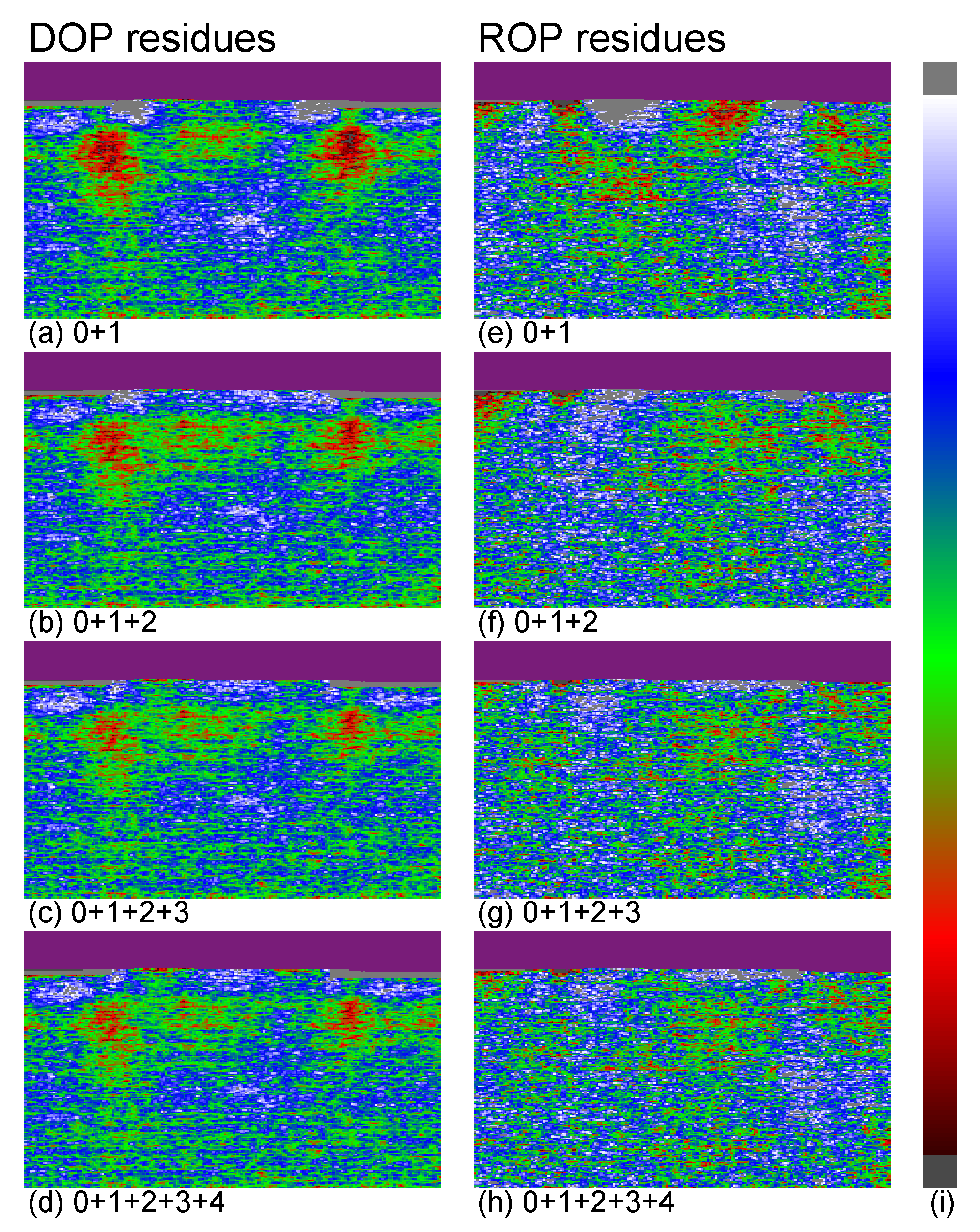
4. Fits of FEM Simulations to the DOP and ROP Data

The width of the SiN stripe was taken to be 4.35 μ m. This value was obtained by comparison of the ROP from 3D FEM simulations [26] of various widths with the ROP data. The horizontal centroids of the ROP lobes near the edges of the SiN were calculated as
h c = i = h c 12 h c + 12 j = 168 175 h i R O P ( h i , v j ) i = h c 12 h c + 12 j = 168 175 R O P ( h i , v j )
for both data and simulations, with R O P ( h , v ) = Y R O P ( h , v ) for calculation of the centroid of the data, and R O P ( h , v ) = i = 1 N s b i f i R O P ( h , v ) + i = N s + 1 N s + 6 b i f i ( h , v ) for the calculation of the centroid of the best fit FEM simulation. The ROP lobes are readily apparent in the bottom panels of Figure 3.
The width as determined from the centroids of the ROP data was 4.75 μ m. Three-dimensional FEM simulations for an SiN stripe width of 4.35 μ m gave the same distance between the centroids of the simulated ROP lobes as for the data. It is clear, from Figure 3 and from the calculation of the centroids, that the ROP lobes lie slightly to the left and to the right of the edges of SiN stripe.
The rms noise for C L DOP and C L ROP measurements was ≈ 6 × greater than a low-noise measurement of the DOP (or ROP) of PL using the equipment and technique described in [13]. The noise sources of the PL measurement system [13] were studied in detail and reported in [28]. The rms noise was 3.1 × 10 3 for the DOP of CL and 3.0 × 10 3 for the ROP of CL, as opposed to 5 × 10 4 for the DOP or ROP from the PL measurement system. The CL noise values were calculated from the averaged data. Assuming white noise, the noise for the raw CL data should be 15 = 3.873 times larger than for the averaged CL data.
The 3D FEM simulations were interpolated on the same h s t e p × v s t e p rectangular grid as the DOP and ROP data, and were then convolved with a unit-area Gaussian function
G ( h i , v j ) = Z 1 exp h i 2 2 s h 2 + v i 2 2 s v 2
to mimic the effects of the finite SEM beam width and the averaging of the data that was performed to reduce the file size. In the equation for the unit-area Gaussian response function, Z is the sum of G ( h i , v j ) on the h s t e p × v s t e p grid and over the assumed extent of the function ( 21 × 33 points), and s h = 209.3 nm and s v = 201.1 nm are scale factors as determined by fits of a Gaussian to the sum of the Gaussians, with scale parameters of 200 nm, in the averaging process that was used to reduce the file size.

4.1. Some Details on the FEM Simulations

The SiN stripe was taken to be 4.35 μ m-wide (in the h ^ direction), 286 nm-thick (= 2 μ m / 7 , in the v ^ direction), and to exist from front to back (along the n ^ direction) of the GaAs substrate. Coordinate scaling in the v ^ direction, with a scale factor of 7, was used to permit efficient meshing of the SiN–GaAs structure [29].
The elastic constants for the SiN were taken to be E SiN = 270 GPa and ν SiN = 0.30 . The value for E SiN is consistent with E SiN found for similarly prepared films [6] and a shallow but smooth minimum in plots of χ T versus E SiN was found at 270 GPa. No well was found for the plots of χ T versus ν SiN . The quality of the fits as visually determined did not seem to depend on the values that were used.
The three non-zero components of the stiffness matrix for a cubic crystal (p. 140, [24]) were taken to be c 11 = 118 GPa, c 12 = 53.5 GPa, and c 44 = 59 GPa for GaAs [30]. The stiffness matrix was converted into a tensor and this tensor was rotated by 45 deg about v ^ and then converted back to matrix form ([24], Chapter VIII) to find the stiffness matrix for GaAs in the plane of a { 110 } facet. These values for the stiffness constants ([31], Table 3.4), which were found by the rotation of the stiffness tensor, were used in the 3D FEM simulations.
Symmetric boundary conditions and coordinate scaling were used to create a rectangular parallelepiped of GaAs that was 200 μ m-wide (in the h ^ direction) by 368 μ m)-thick (in the v ^ direction by 150 μ m-deep (in the n ^ direction) from a 100 μ m-wide by 100 μ m-thick by 75 μ m-deep piece.
The DOP and ROP patterns were calculated for 23 different basis functions, or initial conditions, as explained in Section 1.2. These basis functions included uniaxial and biaxial stresses and strains in the SiN, in the areas beside the SiN, polishing stresses and strains, interface stresses, and the curvatures of the substrate. The approach was to simulate multiple influences and to use the results of the least squares fitting of the simulations to the data to determine the dominant explanations for the measured data.
The first basis function, or dominant explanation, was chosen based on expectations and minimization of χ T . It was expected that the SiN was biaxially strained. To obtain the second dominant explanation, χ T was calculated for each basis function acting with the first one for a total of two basis functions. The basis function that led to the minimum value of χ T was selected. The third and fourth basis functions (or dominant explanations) were selected in a similar manner. Note that selection of the second, third, and fourth basis functions was based solely on the reduction in χ T . There were choices for the second, third, and fourth dominant explanations that were statistically degenerate (i.e., well within one confidence interval) but were not chosen.
The basis functions were not chosen nor made to be orthogonal. Thus, the responses, which were fit to the data, are not expected to be orthogonal. It is expected and observed that there will be correlations between the responses, and that the fit coefficients will change as basis functions are added to the fit ([32], Section 7.3). This makes it difficult to assign a physical interpretation to individual fit coefficients. One needs to interpret the results based on the overall fit.
To ensure that the correlations were not masking the selection of the last three dominant explanations, χ T was calculated for C ( 22 , 3 ) = 22 ! / 3 ! / 19 ! = 1540 combinations of three basis functions along with the chosen first dominant explanation of biaxial stress in the SiN.

4.2. Fits to the Data

Figure 6 shows the DOP and ROP data, the fits to the data for four basis functions, and 5 × the residue, where the residue is defined as the data minus the best fit. The DOP and ROP residues are displayed with gains of g = 50 and g = 75 , respectively.
Figure 7 shows the development of the DOP and ROP residues for the addition of a fitting function. The top panels show the residues for the DOP data and the residue for the ROP data, for a fitting function composed of biaxial stress in the SiN stripe plus background terms. The background terms are polynomials in h and v, as described in Section 1.2, and account for dc offsets in the data and unavoidable artifacts owing to imperfections such as defects, misalignments, birefringence, and polarization-dependent reflections. The just off-scale values for false color images of the DOP and the ROP residues are ± 0.6 % and ± 0.4 % , respectively.
The second panel from the top shows the residues for uniaxial n ^ SiN stress plus a biaxial stress in the SiN (plus background terms). The addition of the uniaxial stress reduces the red `blobs’ under the edges of the SiN stripe, and thus appears to improve visually the quality of the fit.
The third panel from the top shows the residues for biaxial plus uniaxial SiN stress plus a biaxial interface stress between the SiN and the GaAs. The addition of the interface stress appears to reduce slightly the DOP and ROP residues. The changes in the ROP residue are most noticeable in the upper left as compared to the panel above.
The bottom panel shows the residues for the addition of a biaxial stress to the GaAs surface outside of the SiN. This biaxial etch stress does not appear to improve visually the plots of the DOP and ROP residues, and thus does not appear to be a physically significant component in the description of the DOP and ROP patterns.
It should also be noted that the basis functions are not necessarily unique. For the choice of the second basis function, there were eight choices that reduced χ T by the same amount, within four-tenths of one 95 % confidence interval, C I 0.95 . The common effect for these choices was to produce a radius of curvature (i.e., a bowing) on the top surface.
It is clear from the false color images of the residues in Figure 7 that more than one basis function is required to explain the DOP and ROP patterns caused by the presence of the SiN stripe. The DOP and ROP cannot, for example, only be explained by biaxial stress in the SiN.
Table 2 lists the values of χ T = ( χ D O P 2 + χ R O P 2 ) / 2 , χ D O P , and χ R O P for 1, 2, 3, and 4 basis functions plus background terms. The first four rows of the table correspond to the rows of the panels in Figure 7. χ D O P and χ R O P are the reduced chi values for the fits, and are equal to the rms values of the residues. Assuming that the residues are normally distributed, the 95 % confidence interval for χ T , C I 0.95 , is estimated as C I 0.95 = 5.2 × 10 3 for 71 , 316 degrees of freedom ([25], Section 2B).
The bottom row of Table 2 lists the reduced chi values for the background terms only. This row shows that the biaxial SiN stress basis function reduces the rms DOP and ROP residues by large amounts. For example, χ T reduces by ( 2.43 1.0943 258 × C I 0.95 ) with the addition of the biaxial SiN stress basis function. This reduction puts the changes caused by the other terms in perspective. The addition of the second basis function changes χ T by 8.9 × C I 0.95 , some 29 × less than the first basis function. It can also be observed from the last row of Table 2 that the DOP signal, as measured by the DOP rms residue between the biaxial basis function and the background fit, is 3.20 / 1.28 2.5 × larger than the ROP signal. The difference in the magnitudes and extents of the DOP and ROP lobes can be observed by comparing the appropriate panes of Figure 3 and noting that the ROP is displayed with a display gain of 15 × as compared to the 10 × for the DOP.
An analysis of the χ T values of Table 2 shows that the addition of uniaxial n ^ stress to biaxial SiN stress reduces χ T by a statistically significant amount ( 1.0485 1.0943 = 0.0458 8.9 × C I 0.95 ) , that the addition of a biaxial interface stress produces a statistically significant ( 0.0195 3.8 × C I 0.95 ) change in χ T , and that the addition of a biaxial etch stress causes a statistically insignificant ( 0.0016 0.3 × C I 0.95 ) change. These pronouncements on the significance of the change introduced by the addition of a fitting function are similar to the discussions of the preceding paragraphs, which were based on the visual changes in the residues of Figure 7.
The parameter R a , which is the ratio of the ROP to DOP fit coefficients, was taken to be 1.2 . The value for R a of 1.2 gave a minimum value of χ T . R a = 1 is expected if d = 2.4 b , as recommended by Vurgaftman et al. ([23], Table I, p. 5825), and if the analysis presented in Ref. [16] is correct.
A plot of χ T as a function of R a shows that the minimum is smooth, shallow, and broad. For χ T = ± 1.5 × 10 3 = ± 0.3 C I 0.95 , R a = 1.2 ± 0.16 . Clearly χ T is not a sensitive function of R a .
Monte-Carlo analyses were performed to estimate the precision in the value of R a as obtained from the fitting procedure. Gaussian white noise was added to the best-fit DOP and ROP functions to create synthetic data. These synthetic data were used as input to the fitting routine, and fits for R a = 1.15 , 1.16 , 1.25 were performed. The R a value that gave the minimum value of χ T was selected. For noise which gave a χ T = 1.0 for fits to the synthetic data, the average value for R a obtained from 101 different fits with different noise was 1.20 with a standard deviation of zero. A similar result was obtained if the noise was added to the measured data (which already has noise and thus χ T increased to 1.43 ) and the fitting procedure was run. If the rms value of the noise was increased by a factor of 10, the mean value for R a stayed the same but with a non-zero standard deviation, with 88 of the 101 values equal to 1.20 , and with all values in the range 1.19 R a 1.21 .
It seems that additive noise is not the limiting factor in the ability to determine R a from fits to the data. It is likely that the precision in a determination of R a will be determined by the quality of the substrate and the accuracy of the FEM simulations. Defects in the substrate or on the measurement surface, which show as non-uniform regions of DOP and ROP, will likely set limits on the precision of an estimation of the ratio R a from fits to the data. Similarly, FEM simulations with grossly inadequate basis functions or material parameters might lead to bad determinations of R a .
For the fits presented in this work, a value of R a = 1 is expected if d / b = 2.4 and if the simple model [16] underlying Equations (5) and (6) is correct for GaAs. The value of R a found in this work is consistent with the model and the suggested value for d / b ([23], Table I, p. 5825). However, this result is from fits of FEM simulations to single maps, with each map composed of ≈ 36 300 measurements. Confirmation by additional measurements and fits is indicated.
Fits of FEM simulations to measurements of loaded v-grooves etched into an InP substrate gave a value of R a close to unity [25] and this suggests that the combination of the model of strain dependence of DOP [25] and the suggested d / b ratio for InP ([23], Table VI, p. 5829) are reasonable. The InP work comprised fits to multiple independent measurements.

5. Conclusions

The impact of a 4.35 μ m-wide SiN stripe on the local strain of a GaAs substrate was investigated using degree of polarization (DOP) measurements conducted by cathodoluminescence (CL) spectroscopy in a scanning electron microscope. The 3D FEM simulations [29] of 23 different strain states (or basis functions) were made and compared to the measured DOP and four of these basis functions were identified to be the most relevant.
The top four basis functions for the fits were found to be biaxial stress in the SiN, an uniaxial n ^ SiN stress, a biaxial SiN interface stress between the SiN and GaAs, and a biaxial etch strain. The stresses induce a bowing of the GaAs, and this introduces a DOP that varies from the top to the bottom of the substrate. The contribution of the etch stress does not appear to be statistically significant and choices for the influences are not necessarily unique. There were other influences that caused reductions in χ T that were the same within one confidence interval.
The fits are not excellent in that extended red lobes remain under the edges of the SiN stripe and there is a blue band at the top of substrate. These features can be seen in the panels of Figure 7. This suggests that not all influences have been considered in the basis functions that were considered. However, it should be noted that the magnitudes of these influences are likely of the order <1% of the magnitude of the influence of the biaxial stress in the SiN, and thus should not significantly change the values of the dominant fit coefficients. The estimate of 1 % is based on the relative magnitudes of the changes in χ T that are caused by addition of a basis function, c.f., Table 2.
It is interesting to note that the magnitude of the ratio R a of the ROP fit coefficient to the DOP fit coefficient is 1 . A value of R a = + 1 is expected if the expressions for DOP and ROP as presented in (Ref. [16], Section 3.D.4) are employed and if the same convention for the direction for D O P = 1 and R O P = 1 is also employed. For loaded v-grooves on InP, the ratio of the ROP and DOP fit coefficients was found [25] to be consistent with the analysis presented in Ref. [16]. The results for fits to GaAs are consistent with the strain dependence of DOP and ROP that is reported in [16] and displayed in this work as Equations (5) and (6).
The results presented here and in [25], although in need of corroboration, appear to indicate that the dependence of DOP on strain [16], as given in this work by Equations (5) and (6) for GaAs, or as given in [25] for InP, should be used.

Author Contributions

Conceptualization: J.-P.L.; sample growth and characterization: P.P.-R. and M.M.; CL measurements: M.F. and C.M.; simulations and analysis: D.T.C.; original draft preparation: D.T.C.; review and editing: D.T.C., M.F. and P.P.-R. All authors have read and agreed to the published version of the manuscript.

Funding

This research received no external funding.

Institutional Review Board Statement

Not applicable.

Informed Consent Statement

Not applicable.

Data Availability Statement

The data presented in this study are available upon request from the corresponding author. The data are not publicly available.

Acknowledgments

The authors thank François Laruelle for their support and Solène Gérard for help with some of the experiments.

Conflicts of Interest

The authors declare no conflict of interest.

References

  1. Knapp, E.; Battaglia, M.; Jenatsch, S.; Ruhstaller, B. Machine learning assisted material and device parameter extraction from measurements of thin film semiconductor devices. In Proceedings of the Numerical Simulation of Optoelectronic Devices. International Conference NUSOD, Turin, Italy, 12–16 September 2022. [Google Scholar]
  2. Hildenstein, P.; Feise, D.; Ostermay, I.; Paschke, K.; Traenkle, G. Precise prediction of optical behaviour of mechanically stressed edge emitting GaAs devices. Opt. Quantum Electron. 2022, 54, 1–9. [Google Scholar] [CrossRef]
  3. Maina, A.; Coriasso, C.; Codato, S.; Paoletti, R. Degree of polarization of high-power laser diodes: Modeling and statistical experimental investigation. Appl. Sci. 2022, 12, 3253–3263. [Google Scholar] [CrossRef]
  4. Huang, Y.Y.; Chang, Y.H.; Zhao, Y.C.; Khan, Z.; Ahmad, Z.; Hung Lee, C.; Chang, J.S.; Liu, C.Y.; Shi, J.W. Low-noise, single-polarized, and high-speed vertical-cavity surface-emitting lasers for very short reach data communication. J. Lightwave Technol. 2022, 40, 3845–3854. [Google Scholar] [CrossRef]
  5. Yan, Z.H.; Zhou, S. Bonding stress and reliability of low-polarization quantum-well superluminescent diode. Phys. E Low-Dimens. Syst. Nanostructures 2019, 109, 140–143. [Google Scholar] [CrossRef]
  6. Ahammou, B.; Abdelal, A.; Landesman, J.P.; Levallois, C.; Mascher, P. Strain engineering in III-V photonic components through structuration of SiNx films. J. Vac. Sci. Technol. B 2022, 40, 012202. [Google Scholar] [CrossRef]
  7. Liu, J.; Wang, M.; Wang, Y.; Zhou, X.; Fu, T.; Qi, A.; Qu, H.; Xing, X.; Zheng, W. High peak power density and low mechanical stress photonic-band-crystal diode laser array based on non-soldered packaging technology. Chin. Opt. Lett. 2022, 20, 07403. [Google Scholar] [CrossRef]
  8. Yue, Y.; Wang, B.; Wang, X.; Wang, Y.; Xu, P.; Ma, C.; Sheng, X. Study on die-bonding of single emitter high power laser diodes. Opt. Eng. 2022, 61, 036101. [Google Scholar] [CrossRef]
  9. Li, B.; Wang, Z.; Qiu, B.; Yang, G.; Li, T.; Zhao, Y.; Liu, Y.; Wang, G.; Bai, S. Influence of strain on performance of independent emitters in high power quasi-continuous semiconductor laser array. Acta Photon. Sin. 2020, 49, 0914001. [Google Scholar]
  10. Kim, J.; Choi, W.J.; Kim, K.; Kim, D. Nondestructive evaluation of detuned wavelength for as-grown VCSEL epi-wafer. IEEE Photon. Technol. Lett. 2022, 34, 1246–1249. [Google Scholar] [CrossRef]
  11. Colbourne, P.D.; Cassidy, D.T. Observation of dislocation stresses in InP using polarization-resolved photoluminescence. Appl. Phys. Lett. 1992, 61, 1174–1176. [Google Scholar] [CrossRef]
  12. Colbourne, P.D.; Cassidy, D.T. Imaging of stresses in GaAs diode lasers using polarization resolved photoluminescence. IEEE J. Quantum Electron. 1993, 29, 62–68. [Google Scholar] [CrossRef]
  13. Cassidy, D.T.; Lam, S.K.K.; Lakshmi, B.; Bruce, D.M. Strain mapping by measurement of the degree of photoluminescence. Appl. Opt. 2004, 43, 1811–1818. [Google Scholar] [CrossRef] [PubMed]
  14. Coenen, T.; Haegel, N.M. Cathodoluminescence for the 21st century: Learning more from light. Appl. Phys. Rev. 2017, 4, 031103. [Google Scholar] [CrossRef]
  15. Fouchier, M.; Rochat, N.; Pargon, E.; Landesman, J.P. Polarized cathodoluminescence for strain measurement. Rev. Sci. Instrum. 2019, 90, 043701. [Google Scholar] [CrossRef]
  16. Cassidy, D.T.; Landesman, J.P. Degree of polarization of luminescence from GaAs and InP as a function of strain: A theoretical investigation. Appl. Opt. 2020, 59, 5506–5520. [Google Scholar] [CrossRef]
  17. Bahder, T.B. Analytic disperson relations near the Γ point in strained zinc-blende crystals. Phys. Rev. B 1992, 45, 1629–1637. [Google Scholar] [CrossRef]
  18. Bahder, T.B. Eight-band k · p model of strained zinc-blende crystals. Phys. Rev. B 1990, 41, 11992–12001, Erratum in Phys. Rev. B 1992, 46, 9913. [Google Scholar] [CrossRef]
  19. Kirkby, P.A.; Selway, P.R.; Westbrook, L.D. Photoelastic waveguides and their effect on stripe-geometry GaAs/Ga1-xAlxAs lasers. J. Appl. Phys. 1979, 50, 4567–4579. [Google Scholar] [CrossRef] [Green Version]
  20. Cassidy, D.T.; Adams, C.S. Polarization of the output of InGaAsP semiconductor diode lasers. IEEE J. Quantum Electron. 1989, 24, 1156–1160. [Google Scholar] [CrossRef]
  21. Colbourne, P.D. Measurement of Stress in III–V Semiconductors using the Degree of Polarization of Luminescence. Ph.D. Thesis, McMaster University, Hamilton, ON, Canada, 1992. [Google Scholar]
  22. Colbourne, P.D.; Cassidy, D.T. Dislocation detection using polarization-resolved photoluminescence. Can. J. Phys. 1992, 70, 803–812. [Google Scholar] [CrossRef]
  23. Vurgaftman, I.; Meyer, J.R.; Ram-Mohan, L.R. Band parameters for III–V compound semiconductors and their alloys. J. Appl. Phys. 2001, 89, 5815–5875. [Google Scholar] [CrossRef] [Green Version]
  24. Nye, J.F. Physical Properties of Crystals; Oxford Unversity Press: New York, NY, USA, 1985. [Google Scholar]
  25. Cassidy, D.T.; Lam, S.K.K. Degree of polarization of luminescence from facets of InP as a function of strain: Some experimental evidence. Appl. Opt. 2021, 60, 4502–4510. [Google Scholar] [CrossRef] [PubMed]
  26. PDE Solutions, Inc. FlexPDE 7, Version 7.17; PDE Solutions, Inc.: Spokane, WA, USA, 2020. [Google Scholar]
  27. Attolight Webpage. Available online: https://attolight.com (accessed on 1 December 2022).
  28. Lascos, S.J.; Cassidy, D.T. Optical phase and intensity modulation from a rotating optical flat: Effect on noise in degree of polarization measurements. Appl. Opt. 2009, 48, 1697–1704. [Google Scholar] [CrossRef] [PubMed]
  29. Technical Notes. 2022. Available online: https://www.pdesolutions.com/help/coordinatescaling.html (accessed on 1 June 2022).
  30. Dunstan, D.J. Stiffness of GaAs. In Properties of Gallium Arsenide, 3rd ed.; Brozel, M.R., Stillman, G.E., Eds.; Inspec: London, UK, 1996. [Google Scholar]
  31. Landesman, J.P.; Cassidy, D.T.; Tomm, J.W.; Biermann, M.L. Strain measurement. In Quantum-Well Laser Array Packaging: Nanoscale Packaging Techniques; Tomm, J.W., Jiménez, J., Eds.; McGraw-Hill Companies: New York, NY, USA, 2007. [Google Scholar]
  32. Bevington, P.R.; Robinson, D.K. Data Reduction and Error Analysis for the Physical Sciences, 2nd ed.; McGraw Hill, Inc.: New York, NY, USA, 1992. [Google Scholar]
Figure 1. Schematic diagram of the CL measurement system.
Optics 04 00019 g001
Figure 2. A cropped SEM photo of the SiN stripe and GaAs facet. The SiN is on top of the GaAs.
Optics 04 00019 g002
Figure 3. CL yield as calculated from P 1 and P 2 (top panel), DOP (middle panels), and ROP (bottom panels), displayed using a false color mapping. The same DOP and ROP data are displayed in the two columns but for different thresholds of 0.04 × C L max and 0.6 × C L max . The color bar (g) shows the false color mapping that was used to display the data.
Optics 04 00019 g003
Figure 4. Fits of complementary error functions to the C L DOP data as a function of v for: (a) near the mid-point of the SiN stripe, h = 102 ; and (b), far from the SiN stripe, h = 18 .
Optics 04 00019 g004
Figure 5. Fits of complementary error functions to the C L DOP and C L ROP data as a function of v near the mid-point of the stripe, i.e., at h = 102 , and on an expanded scale.
Optics 04 00019 g005
Figure 6. DOP and ROP data, the fits to the data, and 5 × the residues. The same area of 208 × v s t e p = 5.46 μ m by 204 × h s t e p = 8.92 μ m is displayed in each panel. The colour bar (g) shows the false colour mapping that was used to display the data and has the same explanation as the colour bar of Figure 3.
Optics 04 00019 g006
Figure 7. From top to bottom, residues for fits with 1, 2, 3, and 4 basis functions plus background functions. A 3 × 3 point smoothing (unit-area convolution) was used to reduce the noise and thus enhance the ability to see patterns in the residue. Compare panels (c,f) of Figure 6 with panels (d,h) to observe the noise reduction caused by the smoothing. The colour bar (i) shows the false colour mapping that was used to display the data and has the same explanation as the colour bar of Figure 3.
Optics 04 00019 g007
Table 1. Fit parameters for fits of Equation (17) to the CL yields, C L D O P and C L R O P , for vertical planes specified by h. The SiN stripe is in the interval 57 h 156 .
Fileh χ A v e v e (nm) σ v (nm)FWHM (nm)
C L DOP 1846420,817.0 28.45 747201473
C L DOP 9863019,465.2 29.87 785203477
C L DOP 10263019,463.4 29.76 782203478
C L DOP 10667319,452.2 28.46 748205482
C L DOP 19048020,990.3 29.18 766204480
C L ROP 1846421,549.1 26.87 705204481
C L ROP 9866420,073.7 28.24 740203479
C L ROP 10265920,087.5 28.13 737203478
C L ROP 10670520,268.2 26.92 706207487
C L ROP 19246121,603.6 27.70 727206486
Table 2. χ values for fits of the DOP and ROP data to FEM simulations for a 4.35 μ m-wide SiN stripe on GaAs for R a = 1.2 .
ElementsInfluence χ T χ DOP χ ROP δ χ T / CI
0 + 1 1: biaxial SiN stress 1.0943 1.1248 1.0633 258.4
0 + 1 + 2 2: uniaxial n ^ stress 1.0485 1.0757 1.0210 8.9
0 + 1 + 2 + 3 3: biaxial interface stress 1.0290 1.0498 1.0082 3.8
0 + 1 + 2 + 3 + 4 4: biaxial etch stress 1.0274 1.0513 1.0033 0.3
00: background only 2.43 3.20 1.28
Disclaimer/Publisher’s Note: The statements, opinions and data contained in all publications are solely those of the individual author(s) and contributor(s) and not of MDPI and/or the editor(s). MDPI and/or the editor(s) disclaim responsibility for any injury to people or property resulting from any ideas, methods, instructions or products referred to in the content.

