1. Introduction
Wireless power transfer (WPT) is a promising technology that transfers electrical energy from a power source to an electronic load. By eliminating the necessity of physical connectors or wires between the source and the load, WPT systems provide a user-friendly experience and effective charging performance. Therefore, WPT has garnered considerable interest among researchers over an extended period, with current technological breakthroughs further amplifying its significance, especially for electrical vehicles [
1,
2,
3]. WPT users can charge their electric vehicles (EVs) without the hassle of plugging and unplugging cords, which improves their user experience and enables the complete process of automated parking and charging without human intervention.
WPT systems have the potential to be designed to meet the requirements of the charging curve of on-board batteries [
4], which normally includes a constant current (CC) phase, followed by a constant voltage (CV) phase, and finally a cutoff phase [
5]. Using LCC–LCC compensation, WPT systems can maintain a constant charging current that is basically non-variable as the battery voltage rises during CC charging, which is inherent to the system characteristics of LCC–LCC-compensated systems and matches the CC phase perfectly. Once the battery approaches a given voltage level, a constant voltage (CV phase) needs to be maintained, and the charging current has to be gradually decreased to prevent overcharging. Therefore, in the CV and cutoff phases, WPT systems should be capable of adjusting the secondary DC current (the battery charging current) with a constant secondary DC voltage (the constant battery voltage in the CV and cutoff phases). To achieve these charging curve requirements, WPT systems should typically include wireless information transfer (WIT) to continuously send back the battery status (e.g., the charging phase, voltage, and required power) and adjust the control parameters of the power electronics on both sides (i.e., the inverter and active rectifier) in real time.
WPT systems in EV charging applications have specific requirements for the associated communication to ensure safe, efficient, and controllable charging processes. The specific requirements encompass two main aspects:
Real time: The communication should offer real-time capabilities for swift responses and effective control of the system parameters and charging process. This is crucial for monitoring the battery status [
6,
7], adjusting power, detecting foreign objects [
8,
9,
10] and faults [
11], and ensuring system stability during the charging process.
Point-to-point: Especially in scenarios with multiple ground assemblies (GAs) or multiple vehicle assemblies (VAs), the point-to-point nature of near-field communication can be utilized to ensure a reliable pairing mechanism. This avoids mismatches between a GA and a VA and the resulting danger, such as the unloaded and exposed GA operation.
Standard far-field communication technologies typically have higher latency than near-field communication. Wi-Fi latency generally ranges from several milliseconds to 30 ms, while 4G LTE networks provide round-trip latency ranging from 30 to 50 ms, and 5G’s latency can be as low as 1 ms or even lower in ideal conditions. However, 5G requires significantly higher computational power, while near field communication (NFC) can have extremely low latency under 1 ms with low hardware costs. Furthermore, the point-to-point feature of NFC helps the pairing process between a GA and a VA, which is difficult with far-field communication technologies.
Due to the two points mentioned above, many previous studies have investigated the near-field-based communication methods for WPT. A review of the previous works related to the communication for WPT systems is presented in
Table 1. In [
12,
13,
14], the communication signal was modulated using power electronics that reduced the system complexity because no extra digital-to-analog converter (DAC) was needed for signal modulation. However, using this method, the data rate is limited due to the kHz-level WPT frequency used as a carrier for communication. In [
15,
16,
17], the modulated communication signal was coupled with the WPT path using extra analog components so that the frequency multiplexing technology could be applied. However, due to the narrow bandwidth of the analog circuit, the number of carriers was, therefore, limited, which resulted in a low data rate. Furthermore, such communication methods using an HF coupler are typically only suitable for a low-power WPT system because the analog components are in the power path of the WPT system. In this work, a communication method with a higher data rate and a wider frequency band for the kW-WPT system is presented.
2. Fundamentals of LCC–LCC Systems
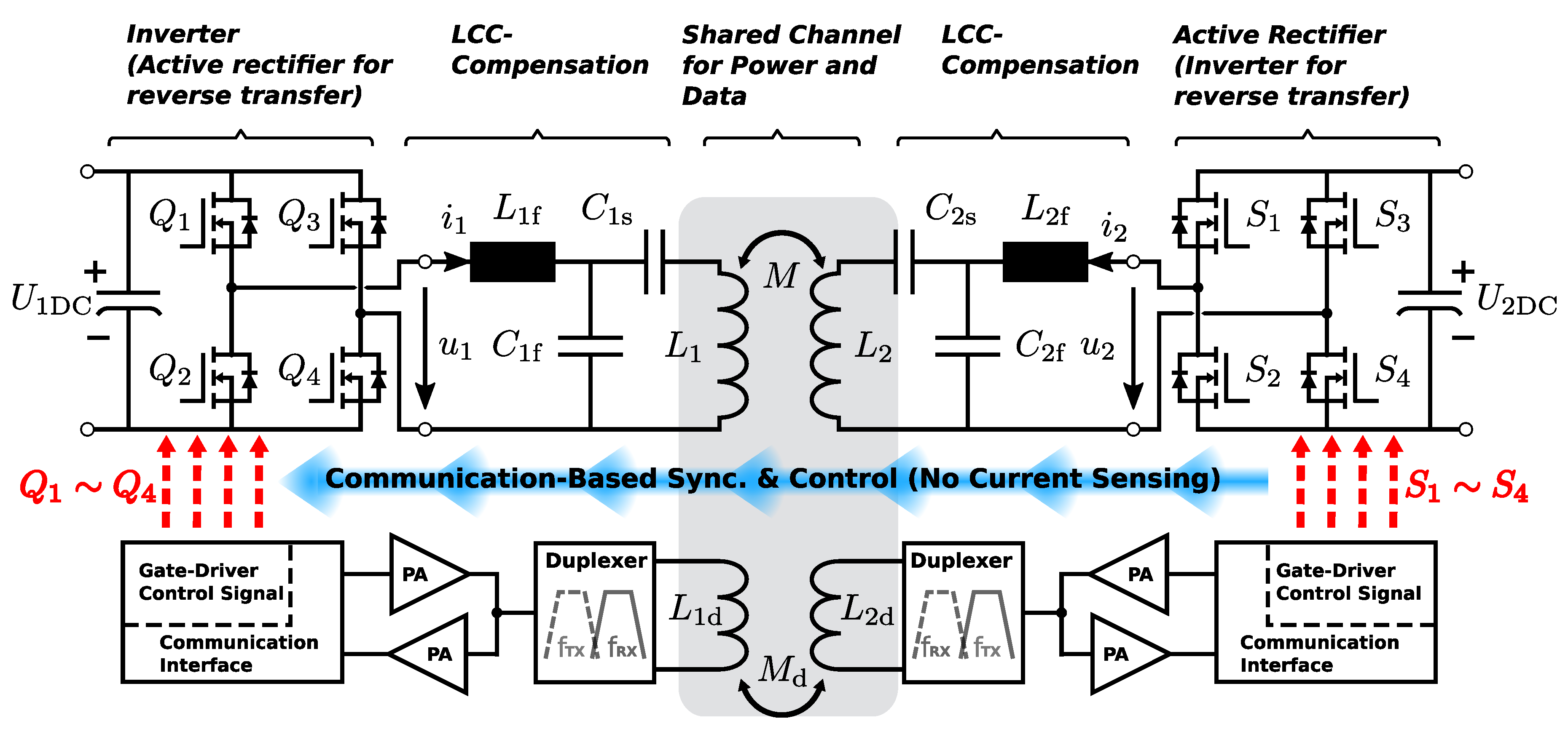
In this section, the WPT part of the system is discussed independently from the communication part. The top side of
Figure 1 shows the LCC–LCC compensated WPT system [
20,
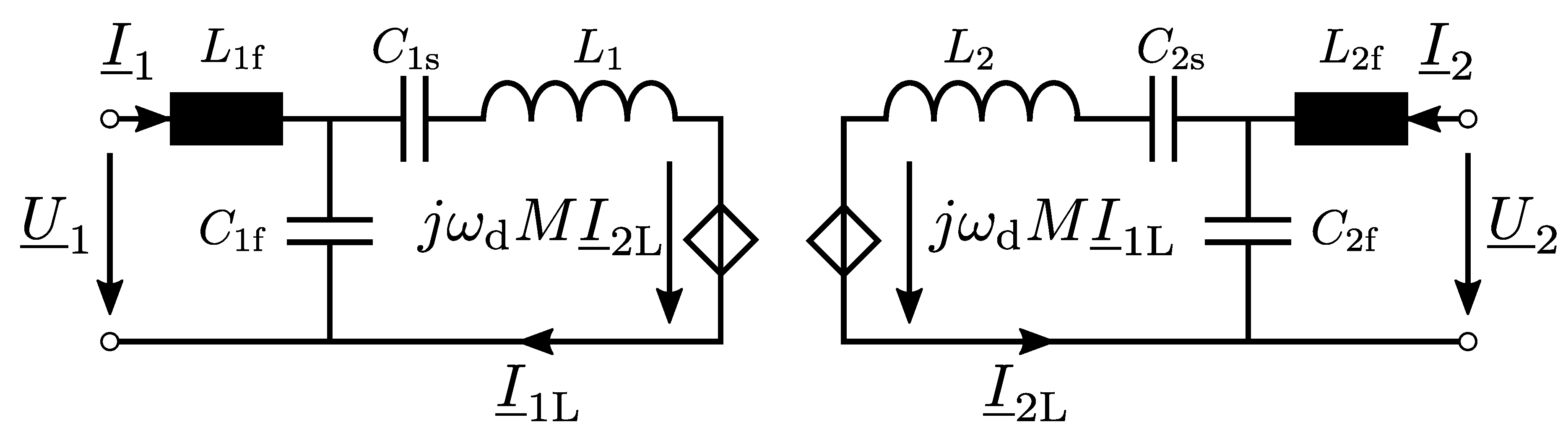
21] with an active rectifier on the right side. The WPT system features a bidirectional power transfer function since both sides are symmetrically designed, as shown in the electric circuit. The components on the left (right) side are identified with notations with indexes starting with 1 (2). The WPT energy direction is signaled with the subordinated communication system. Therefore, an equivalent circuit of the WPT with two voltage sources helps in modeling the bidirectional WPT system, as shown in
Figure 2.
In the following paragraphs, the outside currents of the LCC–LCC-compensated WPT system are first analytically solved by applying the superposition law to the two voltage sources. Based on the closed-form equations of currents, the power of the source and sink can be obtained. Finally, the mathematical relationship between control parameters and system behaviors in terms of transmission power, energy direction, and efficiency are derived.
The design frequency
of a WPT system is usually selected in the 85 kHz band to ensure interoperability between systems. The LCC–LCC-compensated WPT system is usually designed at the frequency of
, and the calculations of compensation components are given as follows.
The input inductances
and
are usually selected to be less than the coil’s inductances,
and
. Therefore, at the design frequency, the three branches have the same impedance, as shown in (
5) and (
6).
The input impedance of the LCC–LCC-compensated network can be derived as follows:
where the impedance of sink
is defined as
The fundamental and
nth harmonic of the primary side voltage
and secondary side voltage
can be calculated using Fourier expansion:
where
n is the number of harmonics, and
is the duty cycles of the primary and secondary side in the range of
.
Based on the impedance calculation in (
5) and (
6) and the fundamental voltages in (
9), the primary and secondary currents
and
are derived as follows:
where
is the loss resistances in the coil paths.
With the calculated input and output currents
and
, the complex power on the primary and secondary side
can be obtained as follows:
and the active power is derived as follows:
By neglecting the loss resistances
and
, the equations above can be simplified as follows:
where the phase difference between the primary and secondary full-bridge voltages
can be used to control the energy flux direction, as shown in
Figure 3. For a forward power transfer, the phase difference
is usually slightly less than
to achieve soft switching, so the primary and secondary active and reactive power can be expressed as follows:
3. Control of the WPT System
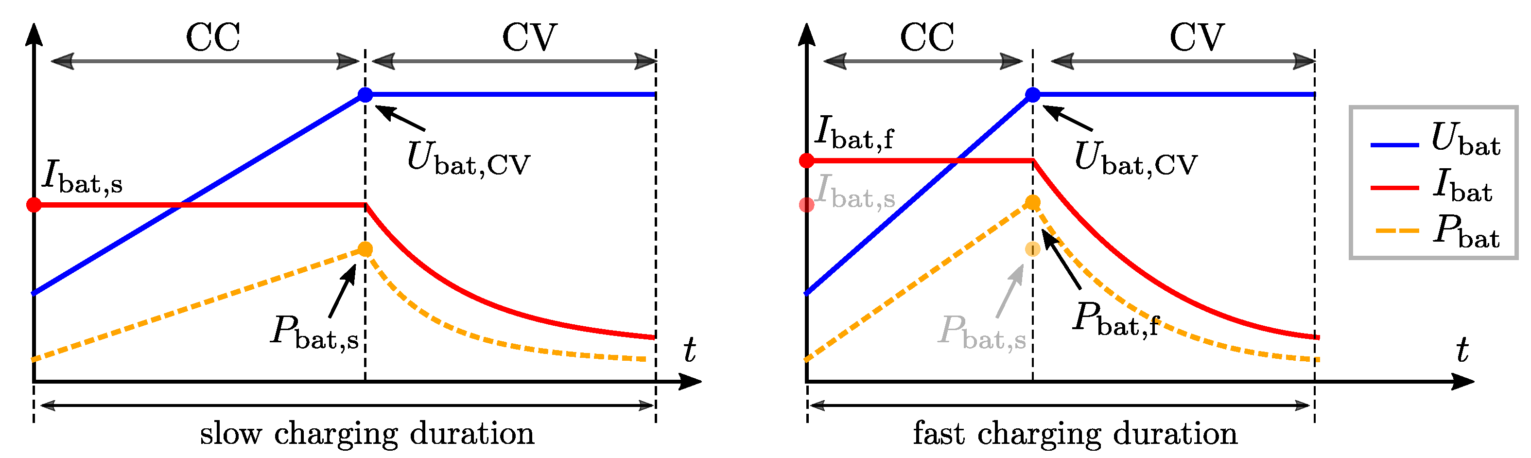
In this section, the control variables that affect the system behavior are introduced. In order to match the charging profile of batteries, the control algorithm should adjust the control variables during the charging process to provide the required current or power in different charging modes (i.e., CC, CV, and the cutoff).
The typical battery charging curve is shown in
Figure 4. In the CC stage, the battery voltage increases, and the peak charging power is reached at the end of the CC phase. After that is the CV stage, during which the charging current needs to be gradually reduced until the battery voltage reaches the cutoff level; then, the charging process is terminated.
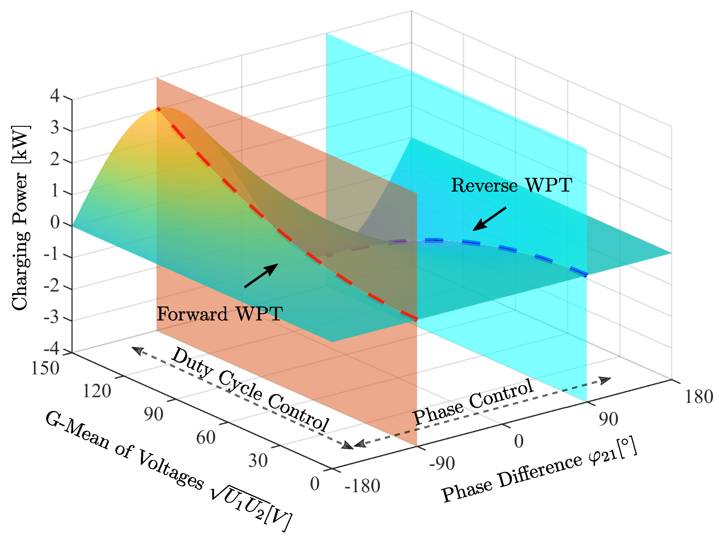
The charging speed or the maximal charging power can be adjusted via the charging current . Therefore, the peak charging power in the fast charging mode is greater than in the slow mode. The control parameters of the WPT system should, therefore, be selected to adjust the charging current, not only for adjusting the charging current for different charging speeds but also for winding down in the CV stage. In this work, the duty cycles on both sides , as well as the phase difference , are selected as control parameters.
The fundamentals of primary and secondary voltages in the form of a function of
can be calculated from (
9) as follows:
By substituting (
20) into (
15), the charging power as a function of control parameters can be obtained as follows:
where
As shown in (
21) and (
22), the charging power increases (or decreases) when the battery voltage
rises (or falls) in the forward (or reverse) power transfer even if the control variables are kept constant. For the forward power transfer, the control variables
and
can be used mainly to match the charging profile.
The maximal forward charging power can be reached by selecting the full duty cycles and adjusting the phase difference to . For the slow charging mode or during the CV stage, the duty cycles can be set to less than 1 to reduce the charging power. And to reduce losses in power electronics, extra reactive power should be added by adjusting to achieve ZVS.
However, to reach the required power, there are multiple sets of solutions of
and
, which provide the freedom to optimize the charging efficiency. With (
14) and (
15), and when the phase difference is set to
, the efficiency of the WPT analog path (i.e., without power electronics) for the design frequency
is obtained as follows:
Based on the equation above, the optimized voltage ratio with maximum efficiency is derived by solving
where
which leads to the following:
As shown in (
27), the LCC–LCC-compensated WPT system has a constant optimized voltage ratio for the optimal efficiency of the analog path at the design frequency.
It is worth mentioning that the control variables need to be adjusted correspondingly during charging to satisfy the optimal voltage ratio to achieve higher AC efficiency. Especially during the CC charging stage, due to the variation in battery voltage (or the secondary DC voltage ), the duty cycles of both sides should be matched constantly to follow the optimal voltage ratio, as well as to provide the required charging power.
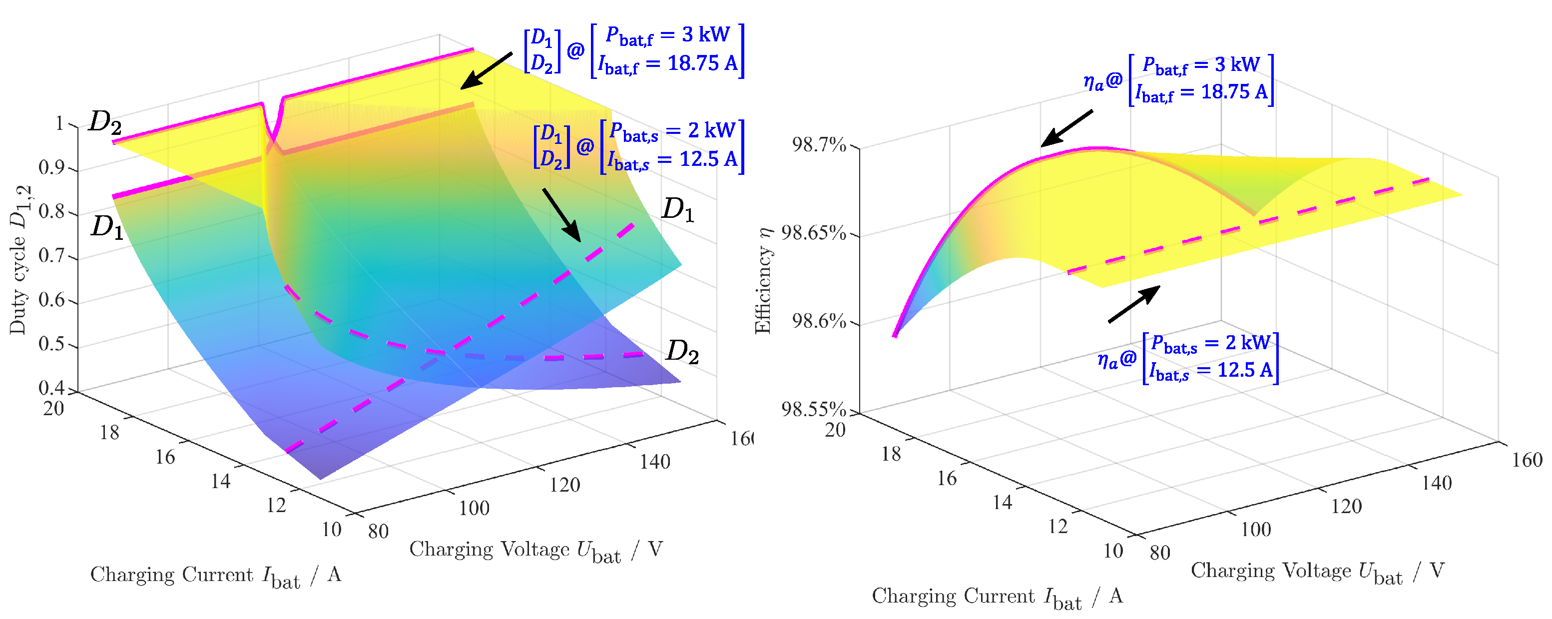
Figure 5 shows the curves of both duty cycles
and
using the proposed optimal voltage ratio to optimize the CC-stage efficiency. The duty cycles in the fast charging mode are illustrated with the two solid lines, which provide a constant charging current of
A. At the beginning, the battery voltage
is too low to satisfy the conditions simultaneously.
The required charging current should be reached ;
The voltage ratio equals the optimal value .
Therefore, the secondary duty cycle
is selected at the maximum to ensure high efficiency, and the primary duty cycle
is tuned to match the required current. In the middle, both conditions can be met simultaneously, so both curves of the duty cycles are adjusted continuously, according to the battery voltage. After that, the optimal voltage ratio condition cannot be met anymore since the battery voltage is increased. Therefore, applying the maximum
and tuning
to match the charging current is the best solution. As shown in the right side of
Figure 5, the maximal efficiency is only achieved in the middle.
For the slow charging mode, both the duty cycles are illustrated with dashed lines. Since the required charging current is lower than the fast charging current, the tuning range of both duty cycles is wider. For the illustrated 2 kW charging, the optimal voltage ratio can be achieved for the entire CC stage, and the optimal efficiency is reached all the time, as shown in the right side of
Figure 5. However, due to narrow duty cycles, the switching losses of the power electronics will increase, and these increases can be reduced by introducing more reactive power via a tuning phase difference,
.
This proposed control algorithm requires information on the charging profile and the co-control of full bridges on both sides. In this work, a near-field-based communication between a primary and secondary WPT system is introduced, which enables the synchronization of both full bridges, the information transfer between both sides, and the co-control of the inverter and the rectifier. Based on near-field communication, the switching frequency of both full bridges is synchronized periodically, and the phase difference is set directly. Complex current sensing and current-based synchronization are, therefore, not required.
4. Hardware for Near-Field-Based Communication in the WPT System
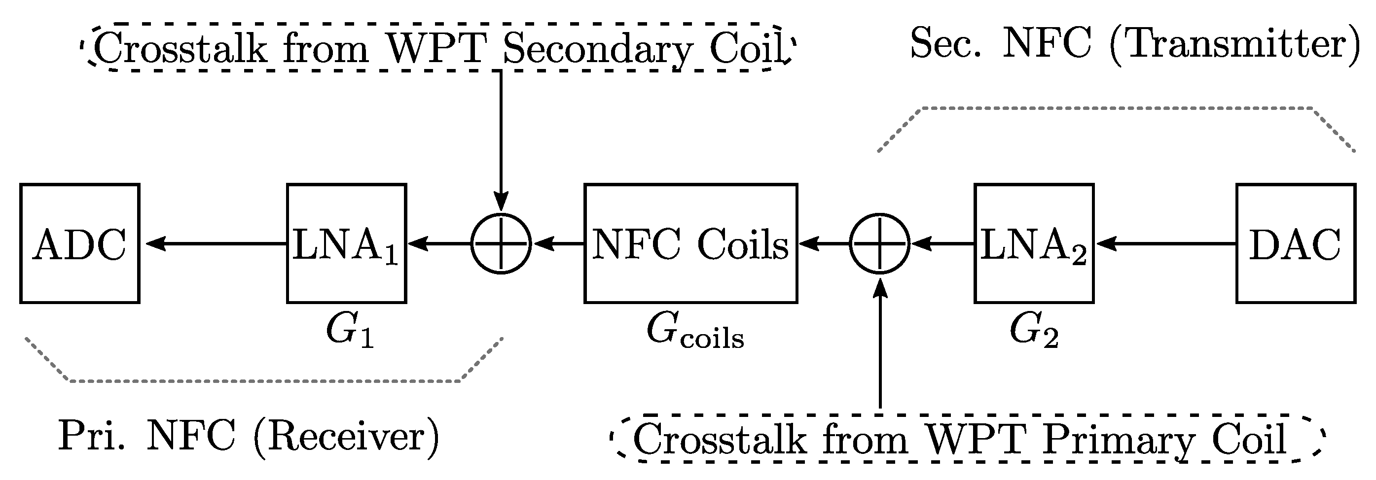
The main challenge of integrating near-field-based communication into a WPT system is the crosstalk from the WPT system, in which the kilowatt-WPT field and the milliwatt-communication signal share the same space and time. First, the fundamentals of the WPT system could induce a voltage on the coils of near-field-based communication. However, in the frequency domain, the frequency of this induced voltage is much lower than the carrier frequency used for communication, so it can be easily filtered out and, therefore, does not interfere with demodulation. Nonetheless, the high amplitude of the induced voltage may overflow the voltage range of the ADC, preventing the overlaid high-frequency communication signal from being sampled. This leads to the loss of information or even damage due to the high induced voltage on the electronics. Second, high-frequency noises generated via the switching of MOSFETs could lead to errors in communication.
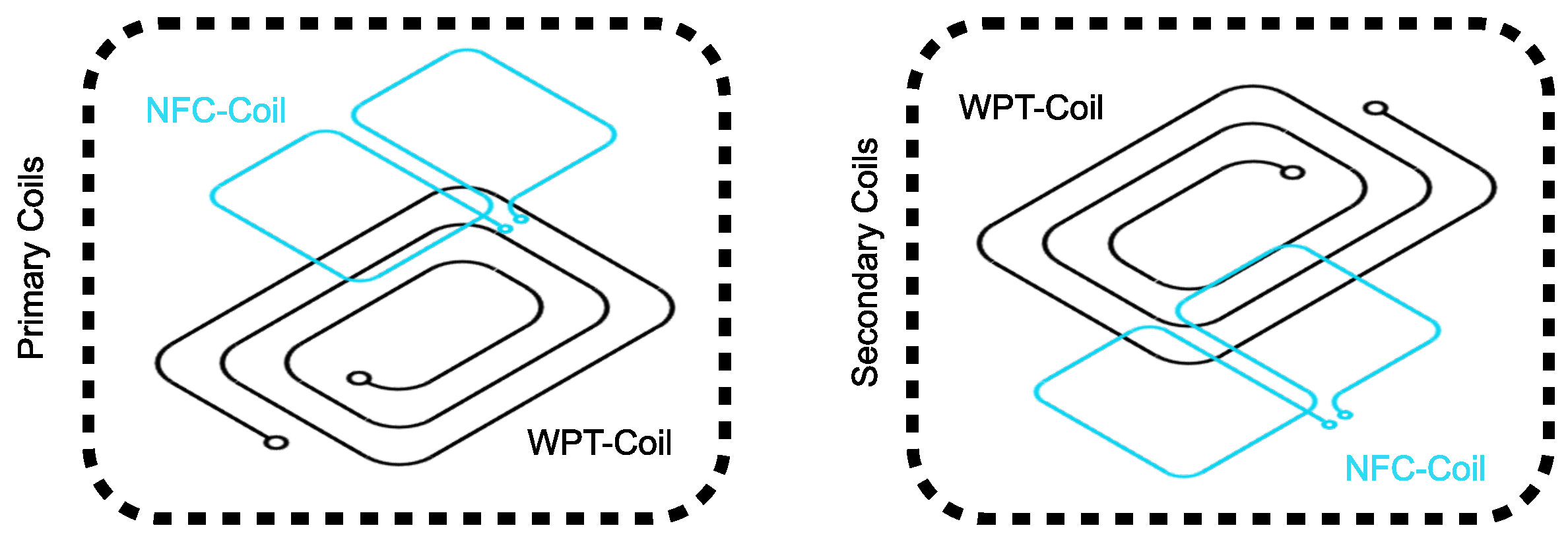
To deal with the crosstalk from the WPT fundamentals, the double-D coils of the wireless communication are designed to be center-aligned with the WPT coils so that the induced voltages from the same side of the WPT coil on the left and right parts of the double-D coils cancel each other out, as shown in
Figure 6. This layout minimizes the crosstalk from the WPT coil to the communication coil on the same side. However, the crosstalk from the WPT coil on one side to the communication coil on the other side is only minimized when they are well aligned. Therefore, an extra analog filter in the low noise amplifier (LNA) is used to suppress the induced voltage via misalignment to ensure the received signal on the ADC does not overflow. And in the FPGA program, the WPT system can be turned off when the ADC of the communication system receives a high amplitude greater than the threshold, which will protect both the WPT system and the communication system when the coils are largely misaligned. Additional high-order digital filters are implemented in the FPGA to improve the quality of demodulation.
To deal with the high-frequency noise from the switching of MOSFETs, the power of communication can be enhanced, which improves the signal–noise ratio (SNR). As shown in
Figure 7, the FPGA-modulated digital signal is generated via the transmitter DAC, amplified via the first LNA, and then goes through the double-D coil system, amplified via the second LNA, and it is finally sampled by the receiver analog-to-digital converter (ADC) for demodulation. Therefore, the gain of the signal path can be expressed as follows:
Since the voltage range of DAC and ADC is
peak-to-peak, the total signal gain
should be less than 0 dB; otherwise, the input of ADC will overflow. The maximal gain of the NFC channel is measured at a perfectly aligned position; therefore, the gain of both low noise amplifiers in the communication frequency band should meet the following condition:
The noise from the WPT primary and secondary sides is coupled with the communication chain. The first noise path starts from the primary WPT coil, which is then coupled to the secondary NFC coil and transmitted through the primary NFC coil and LNA; finally, it is received by the receiver ADC. The second noise from the secondary WPT is merged into the communication path directly from the primary NFC coil. The crosstalks of the primary WPT coil to the primary NFC coil, as well as the secondary WPT coil to the secondary NFC coil, is minimized and, thus, negligible, as mentioned above. Therefore, the gain of the noise paths can be expressed as follows:
To improve SNR, the gain of the LNA transmitter should be increased, and the receiver LNA should be used to adjust the voltage range in order to ensure that the ADC input voltage is less than the voltage limit.
Depending on the noise profile, a guard interval in time or frequency can be applied. For instance, if the switching noise covers the frequency band of subcarriers, then subcarriers with other frequencies can be used to avoid communication errors. If the total available frequency band is covered by noise, then setting a time guard interval is necessary, which means the communication only occurs after the switching time points.
5. Software of Near-Field Based Communication for the WPT System
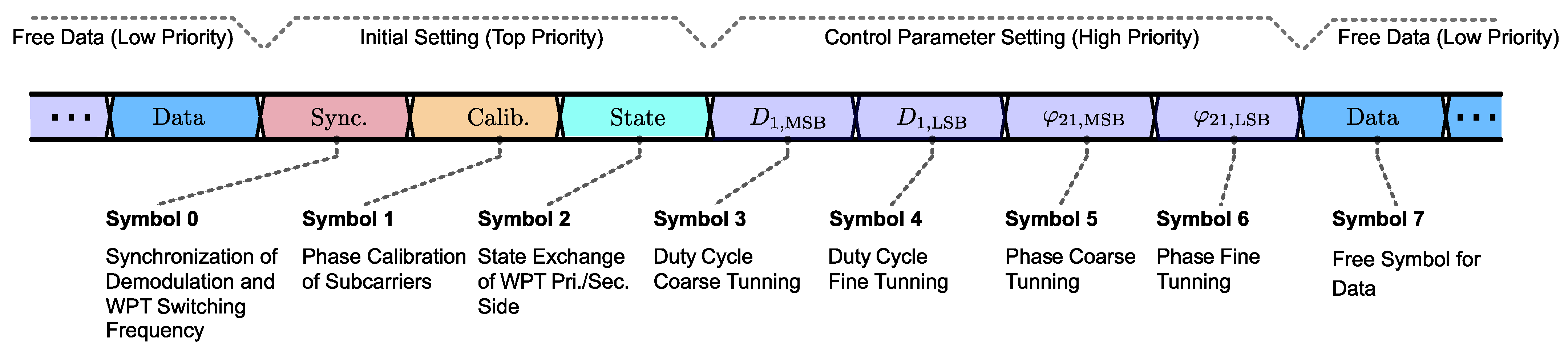
In this section, the software that was implemented in FPGA for near-field communication is presented. The proposed near-field communication is based on orthogonal frequency division multiplexing (OFDM), using multiple subcarriers with different frequencies to transfer information. Only binary-phase shift keying (BPSK) was applied in this work to ensure the robustness of the communication; however, multiple PSKs can also be applied to improve the data rate when necessary. The synchronization in the time domain and calibration in the frequency domain are implemented so that the communication also works when misalignment occurs or in non-stationary scenes. Besides the symbols of synchronization and calibration, all the other symbols are used to transmit information, while the upcoming five symbols are reserved for the WPT state and control parameters. One data package is illustrated in
Figure 8.
The initial symbol (Symbol 0) synchronizes the to-be-demodulated receiver signal so that the start point of the receiver signal can be determined roughly. The start point is important to the demodulation process because an earlier or later start point leads to a phase shift of the by fast Fourier transform (FFT) processed signal in the frequency domain or an intersymbol interference, which results in a flash-bit decision. The synchronization signal transmitted through the NFC coils is modulated as a superposition of several frequency-selectable sinusoidal functions:
where
and
are the amplitudes and phases of the
frequency components, and
is the number of sample points. The modulated signal is repeated
times:
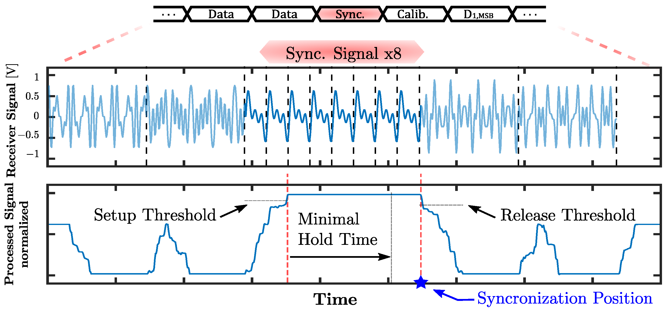
The generated synchronization signal is shown in the first row of
Figure 9, and the second row shows the result of the auto-correlation. The auto-correlation of the signal can be expressed as follows:
where
is the distorted signal due to the NFC channel.
During the periodic repetition of the synchronization signal, the previous equation is kept constant until the “Sync.” signal runs out and the signal in the next symbols comes up. The value of the constant stage can be obtained as follows:
where
is the changed amplitude of the frequency component due to the NFC channel.
Since the synchronization signal is generated on one side and the end of the signal can be detected on another side, both sides of the WPT system can, thus, be synchronized. To detect the synchronization (i.e., the end of the “Sync.” signal), the parameters “Setup Threshold”, “Minimal Hold Time”, and “Release Threshold” should be set appropriately, which mainly avoids the false trigger of synchronization. Different parameters can lead to a shift in the synchronization position; however, the phase shift is compensated in the “Calib.” stage.
In symbol 1 (the calibration symbol), the phases of all subcarriers are pre-defined on both the transmitter and the receiver. On the receiver side, the phase shift due to the synchronization position drift can, therefore, be estimated. For the WPT part, the synchronization position is compensated for via the estimated time shift, which avoids the coil misalignment resulting from a synchronization position offset. For the communication part, the phases of all subcarriers in the calibration stage can be used as phase references in the demodulation for the upcoming symbols. Therefore, the coil misalignment will not affect the bit decision later with the data symbols.
Symbol 2 is reserved for informing the receiver side about the WPT-related status of the transmitter side. In this work, 2 bits were used to indicate the power transfer status:
“00”: the active side (referring to the NFC transmitter) is not ready for WPT;
“01”: the active side is only ready for forward WPT;
“10”: the active side is only ready for reverse WPT;
“11”: the active side is ready for both directions of WPT.
The next four symbols are reserved for the transmission of the WPT control parameters on the receiver side. In this work, up to 60 subcarriers can be used, each modulated via BPSK. The communication system was tested with four and eight subcarriers, for which the achieved data rates were 0.66 Mbsp and 1.32 Mbsp, respectively. The four-subcarrier-version achieved better SNR than the eight-subcarrier-version because the available amplitude of each subcarrier that equaled the maximal DAC voltage range divided by the number of subcarriers was greater. To achieve high tuning resolution in the duty cycle and phase offset, two symbols (8 bits or 16 bits) were reserved for each control parameter.
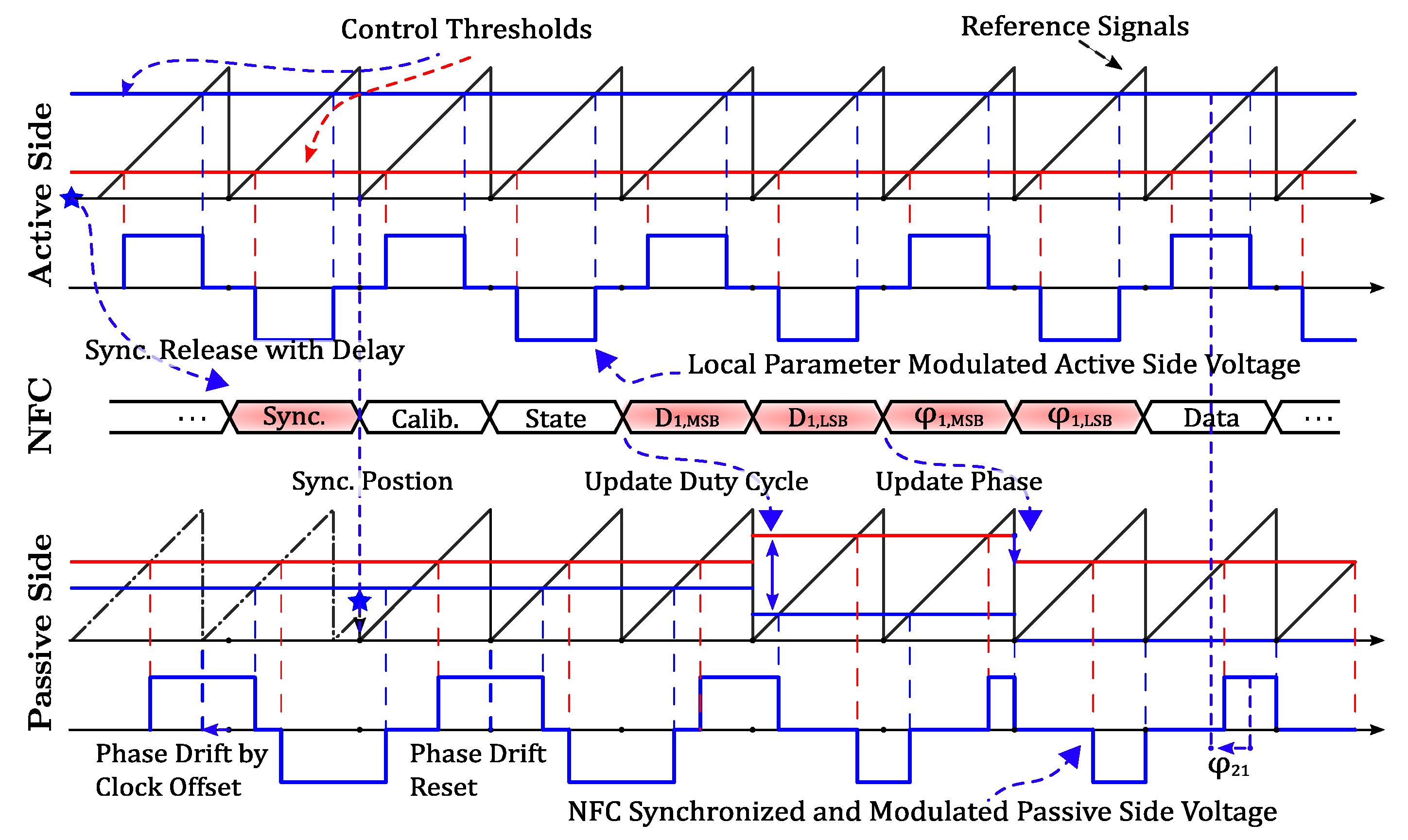
The timing diagram in
Figure 10 shows one complete tuning process. The active side’s control parameters are unchanged, and the maximum value of the sawtooth signal determines the active side-switching frequency. The blue and red lines are control thresholds together with extra flip-flops, and the two gate signals of both high-side MOSFETs on two half-bridges are generated. As a result, the distance between the blue and red lines determines the duty cycle of the resulting voltage wave, which is illustrated in the second row. The NFC signal is modulated and transmitted simultaneously with the gate signal generation; thus, the passive side’s WPT synchronization and control parameters are updated, which is shown in the middle of the figure.
In the beginning of the sawtooth signal that is modulated on the passive side via its onboard crystal, a slight phase drift referring to the primary sawtooth signal is illustrated. The phase drift is due to the frequency tolerance of two crystal oscillators on both sides. Therefore, the synchronization signal is applied periodically to reset the passive side counter (i.e., the sawtooth signal), which is marked with the blue star. During the stage of control parameter adjusting, the blue and red lines are adjusted correspondingly to achieve the required duty cycle and phase of the passive side.
6. Prototype and Experimental Setup
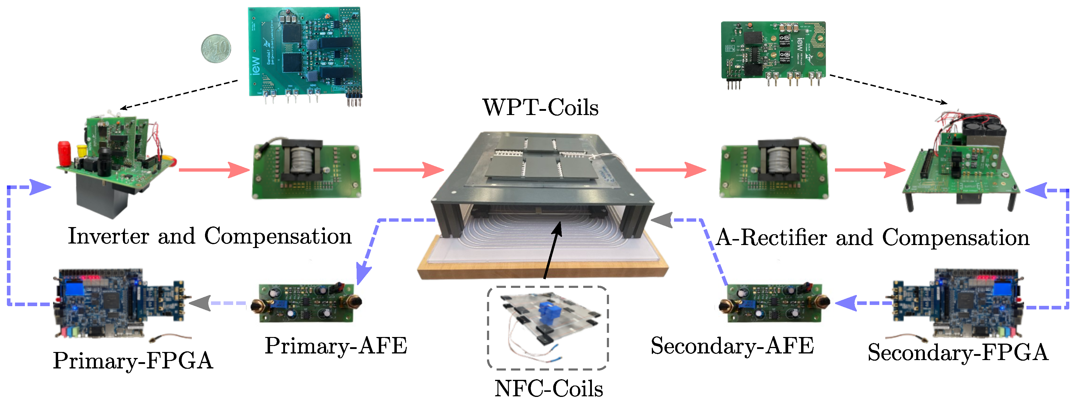
A prototype was implemented based on the WPT and near-field communication components outlined in the previous sections. A system overview is shown in
Figure 11. For the WPT part, both the primary and secondary sides are equipped with full-bridge circuits to provide the functionality of a bidirectional power transfer. The primary full bridge was implemented using four 600 V GaN FETs from Texas Instruments with part number LMG3422R030. The secondary full bridge is powered with four 650 V enhancement mode power transistors from GaN Systems, part number GS66508B. Using GaN technology, the inverter and rectifier have more potential to be downsized and can achieve lower hard switching losses than some conventional semiconductor technologies.
The LCC compensation networks of both sides were implemented in Print Circuit Board (PCB), and the resulting values of each component are given in
Table 2. Multilayer ceramic capacitors from TDK with C0G as dielectric elements were surface-mounted on the PCB. And ferrite cores with part number 495-5501-ND from TDK were used for the filter inductors
.
The coil system was designed according to the SAE J2954’s Z1 class with a coil distance of about 130 mm. On top of the primary WPT coil and on the bottom of the secondary WPT coil, the communication coils were installed. Both communication coils were designed as double-D coils, as shown in
Figure 6. The outside dimensions of the communication coils on both sides are about 28 mm × 28 mm. Only one turn of winding was used for each coil. The position of the communication coil with reference to the WPT coil was adjusted so that the coupling between them was minimized. For the near-field communication, each side has an analog front end. An amplifier and filters were integrated into the PCB to protect the frequency band of communication from crosstalk due to the WPT. A non-inverting amplifier using LM7171 from Texas Instruments and ICL7662 from Analog Devices for dual supply were implemented. The secondary amplifier gain was configured at about 16 dB, the primary amplifier is about 0 dB, and the measured gain of the communication coil system in the frequency band is less than −16 dB. The transmitter signal, which is modulated on the secondary FPGA, is filtered and amplified via both amplifiers and finally received and demodulated via the primary FPGA. The FPGA board (DE10-Standard with Intel Cyclone
® V SE 5CSXFC6D6F31C6N) on each side is used for modulation and demodulation for the near-field-based communication, as well as the generation of control signals for the full bridge.
7. Experimental Results
In this section, the proposed combined information and power transfer system is verified. The WPT transmitter DC voltage is provided by an EA-PS8500-60 power supply. The WPT receiver is terminated on an electronic-load EA-ELR 9750-22. The waves of the WPT and near-field communication were acquired using a Yokogawa DLM4038 oscilloscope.
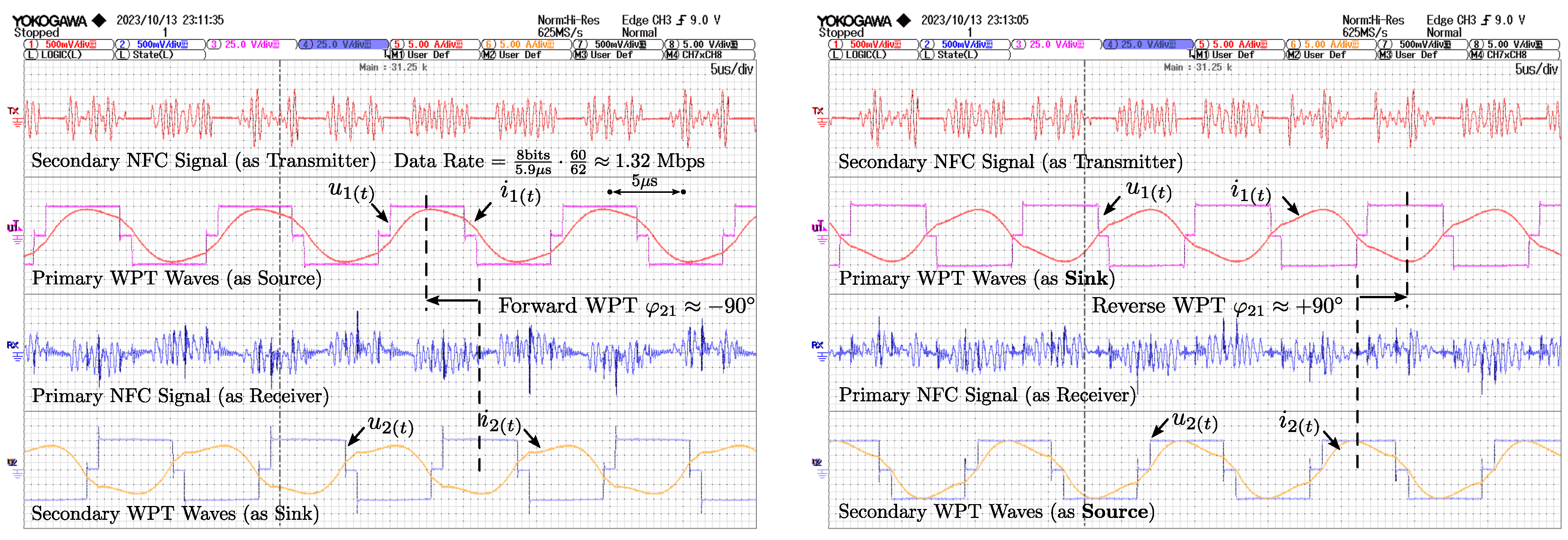
The forward and reverse WPT modes are presented in
Figure 12. On the left side, an overview of the NFC transmitter and receiver signals, as well as the WPT voltage and current waves for the forward power transfer, are given. The WPT primary side was synchronized using the communication signal transmitted from the secondary side to the primary side. The primary voltage phase was adjusted about
ahead of the secondary phase for the forward power transfer. The primary parameters (the phase and the duty cycle) were extracted from the communication data packages. On the right side of the figure, the primary voltage phase was set to about
behind the secondary phase; thus, the phase difference of the secondary voltage current was about
shifted. Therefore, the power direction was reversed.
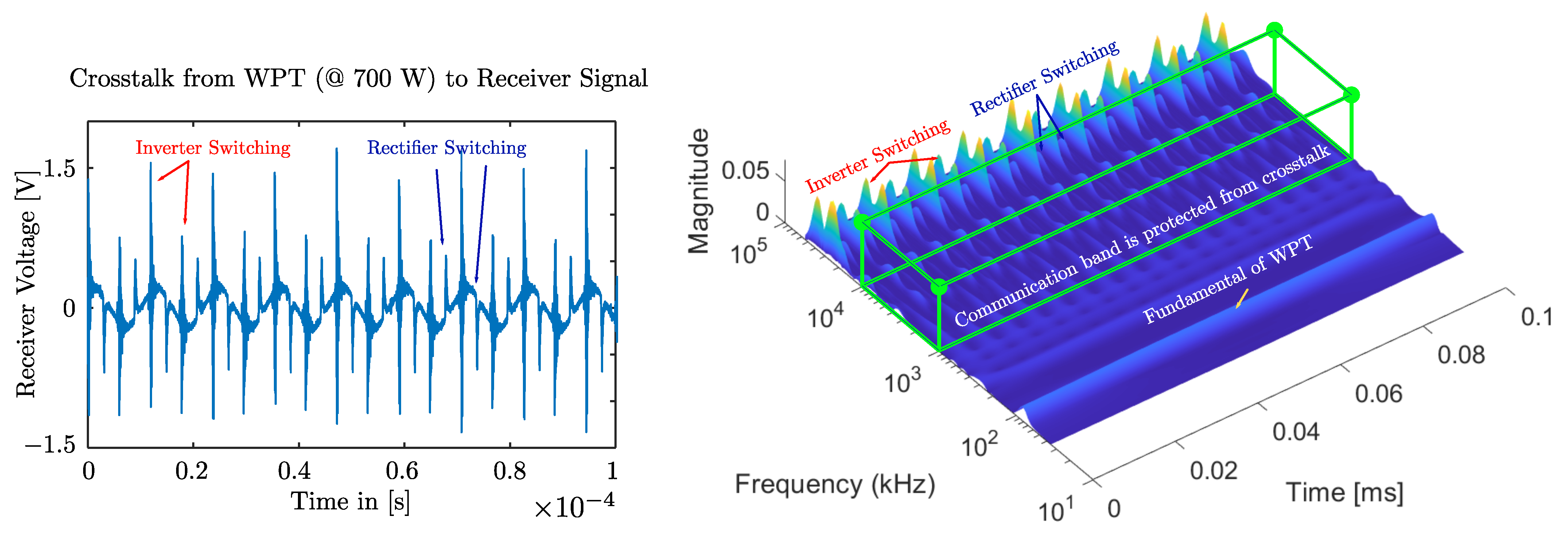
Figure 13 shows the measured crosstalk at the WPT power of 700 watts. The receiver signal is acquired without a transmitter signal, the external synchronization signal is applied to the inverter and rectifier, and both operate at a full duty cycle, so pure noise from the WPT system is recorded. As shown in the right figure, the crosstalk magnitudes in the communication frequency band are low, so the communication is well protected. However, with significantly increased WPT power, the crosstalk magnitudes will further increase, which could lead to an error in communication. One potential solution is to reduce the number of subcarriers so the amplitudes of each of the subcarriers can be sufficiently higher than the amplitudes of the crosstalk; therefore, the communication is robust.
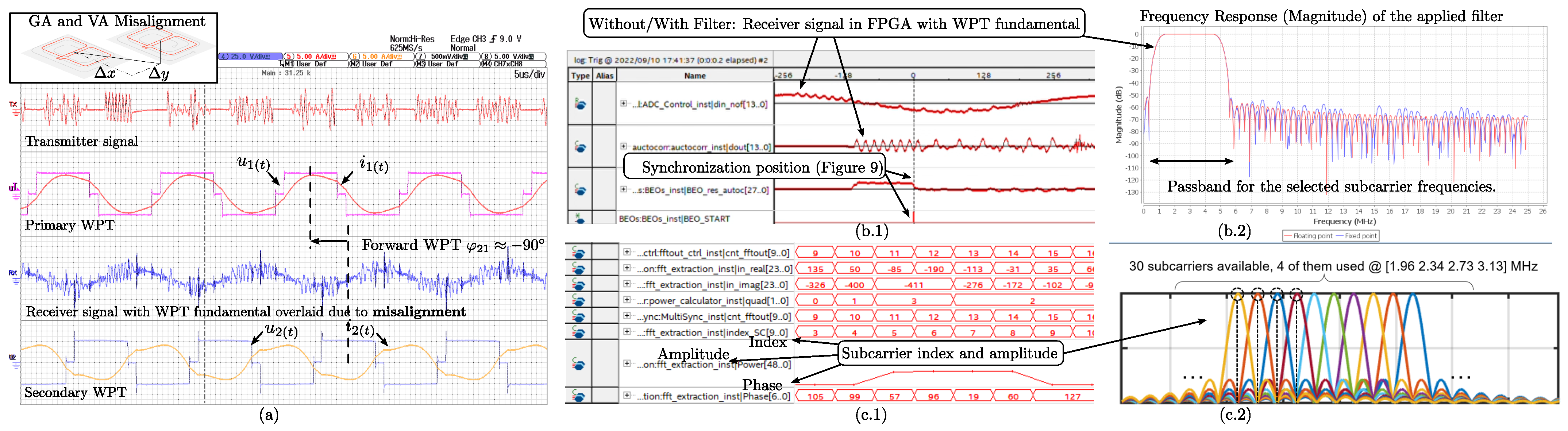
Besides the signal overview for the aligned position, the effects that resulted from misalignment (a position offset between the primary and secondary coils) are presented in
Figure 14. As shown in
Figure 14a, due to misalignment in the x and y directions, a sin-wave due to the WPT fundamental was overlaid on the receiver signal (third row). The overlaid noise was well suppressed via the digital filter implemented in the FPGA, and the filtered signal is shown in the second row of
Figure 14b1. It ensures that the auto-correlation result not be affected (third row); thus, the synchronization is precise and robust in misaligned positions.
A fixed-point digital bandpass filter with a 150th order was implemented in the FPGA, and the frequency response is presented in
Figure 14b2. The cutoff frequencies are set based on the subcarrier frequencies.
In
Figure 14c1, four subcarriers with indexes 5, 6, 7, and 8 (frequencies of 1.96, 2.34, 2.73, and 3.13 MHz) from the FPGA signal taps are presented. The amplitudes at each subcarrier frequency (the second-last row labeled as “power”) correspond to the theoretical separate amplitudes in
Figure 14c2, which indicates that the subcarriers are orthogonal to each other.
The latency is measured using the FPGA signal tap that sends back real-time logic signals from the FPGA to a computer. The throughput latency of the communication (i.e., from the input of digital bits in modulation to the output of digital bits in demodulation) consists of 5.12 µs from IFFT in modulation, 5.12 µs from FFT in demodulation, 2.56 µs from the digital filter, as shown in the first and second rows in
Figure 14b1, and several short delays due to a signal buffer and operations in the FPGA. The total latency of communication was measured at about 15.36 µs. By reducing the symbol duration, the latency can be further improved.
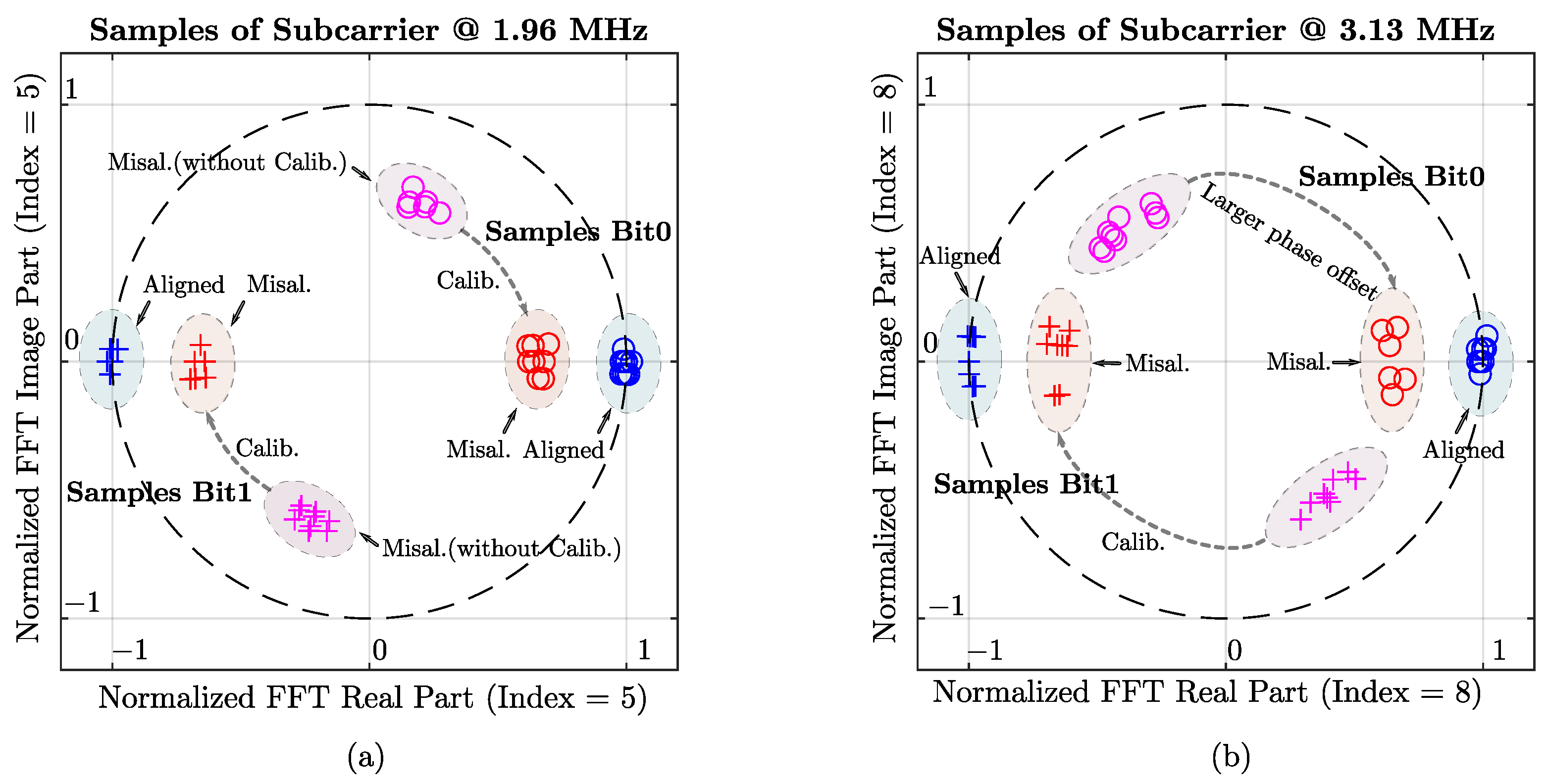
The demodulation is processed in the FPGA, and the receiver signal is first segmented based on the synchronization position and symbol positions; then, the FFT of the segmented signal is calculated. Finally, the results of the FFT (the real and image parts) are used for bit decisions.
Figure 15 shows the constellation diagrams of subcarriers at 1.96 MHz and 3.13 MHz, recorded from FPGA signal taps. The distribution of subcarriers with a higher frequency is wider than that of the subcarriers with a lower frequency because the same time offset results in a greater phase offset for subcarriers with a higher frequency. Comparing the red and blue marks revealed that misalignment resulted in a decrease in amplitude (i.e., closer to the origin) and had approximately no impact on the angle and, thus, no impact on the bit decision. The amplitude variation can be further re-used for the positioning of the GA and the VA.
Based on the near-field communication between the primary and secondary sides, the WPT system was measured at different operating points to simulate the charging process.
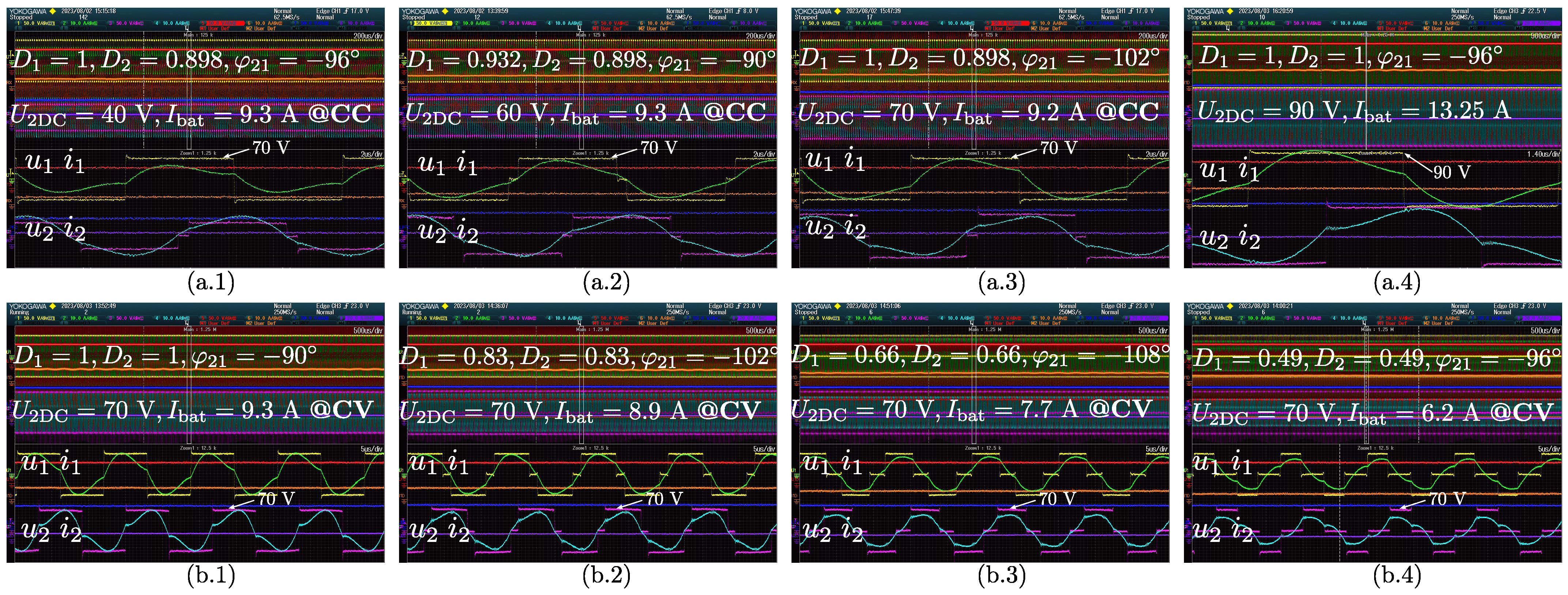
Figure 16 shows the WPT waves of some typical operating points. In the first row (a.1), (a.2) and (a.3) show the waves for the CC stage; with
V presented, the current is constant near
A, and 1.2 kW charging power is captured, as shown in (a.4), with increased DC-link voltages,
V. In the second row, from (b.1) to (b.4), the waves of the CV stage are presented. The secondary DC voltage is constant,
V, and the current is reduced step by step using control parameters. Figures in the second row show four typical currents ranging from 9.3 A to 6.2 A.
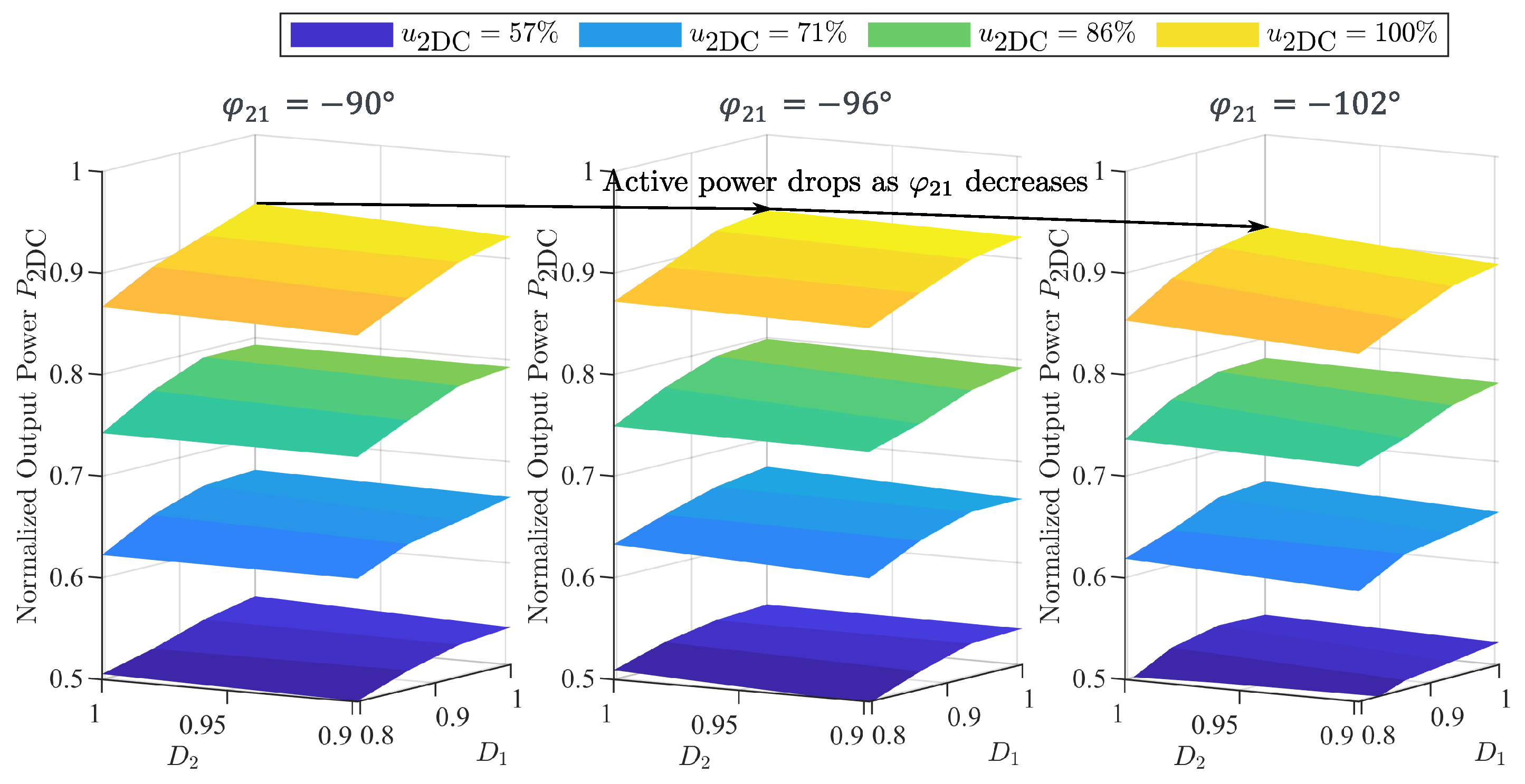
Figure 17 shows an overview of the charging power variation due to the battery voltage increasing during the CC stage. The duty cycles of both full bridges are used to adjust the charging power. Three different values of the phase difference between the primary and secondary voltages are applied, which shows that setting the phase difference away from
results in a reduction in the active power.
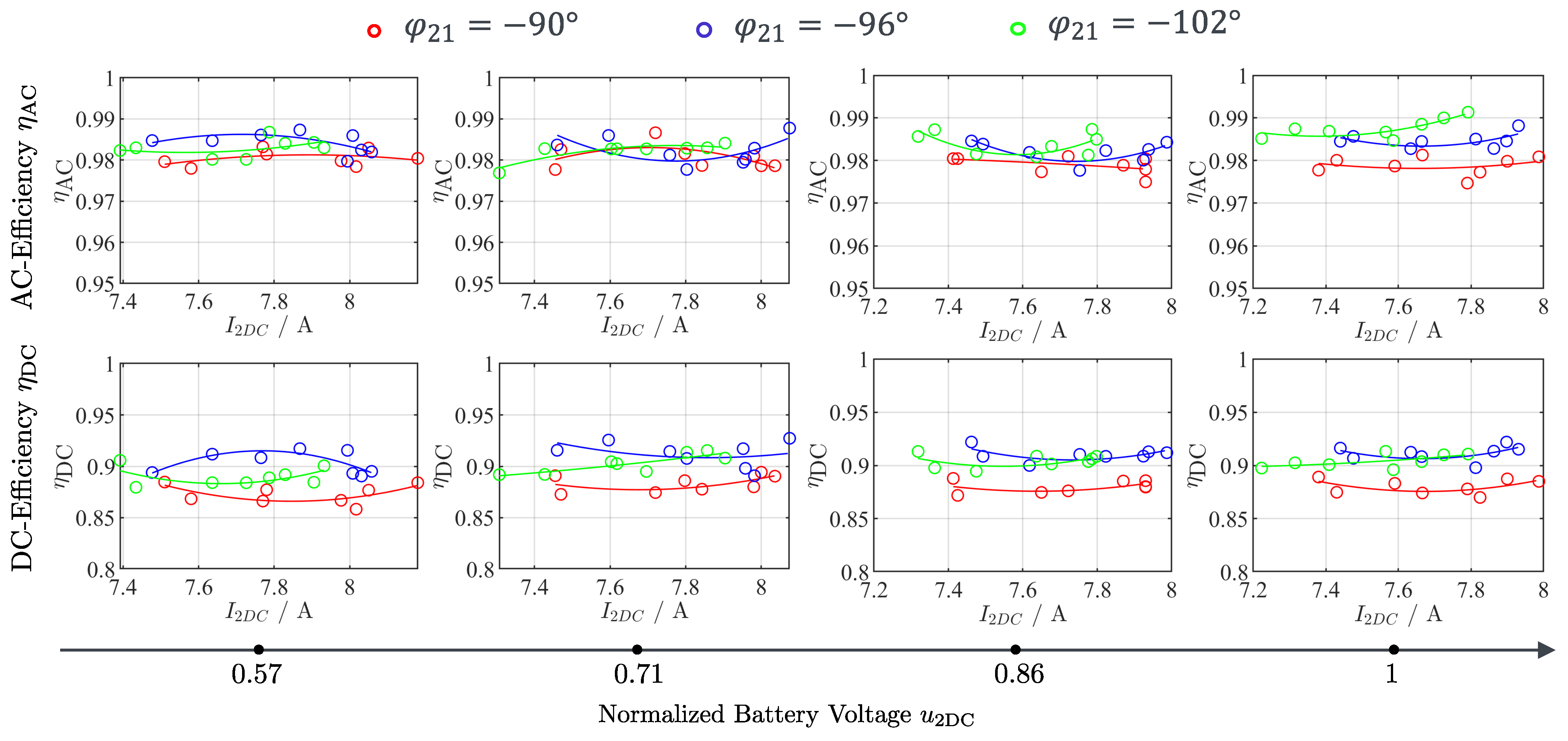
Besides the charging power, the efficiencies (i.e., AC efficiency and DC efficiency) are presented in
Figure 18. The required charging current for all three battery voltage levels was achieved by tuning the duty cycles according to the optimal voltage ratio, as given in (
27). As shown in the first row of the figure, the AC efficiency can be kept nearly constant above 97% and does not much depend on the phase difference
. However, the DC efficiency shows a dependence on the phase difference. As shown in the second row of the figure, the DC efficiency of
is better than the other two data sets with a phase difference of
and
. In the
case, the reactive power at the input and output of the analog WPT path is nearly zero, so the zero-voltage-switching (ZVS) cannot be reached. By decreasing the phase difference to
, the ZVS conditions can be met.
By further reducing the phase difference, the third quadrant current in the GaN-MOSFET during deadtime increases. It is worth mentioning that the GaN-MOSFETs have no intrinsic p–n junction body diode; the third quadrant current builds up a reversed to enable the third quadrant current flows from the source to the drain in saturation. Therefore, by further reducing the phase difference, higher losses due to the third currents in GaN-MOSFETs can be produced. Unlike with conventional semiconductors (e.g., SiC), a reverse conduction voltage of up to due to off-state third quadrant current was obtained with the GaN-MOSFETs. Parallel diodes can be considered to reduce the losses in GaN-MOSFETs due to the third current at the cost of extra output capacitance.
8. Conclusions
Combined wireless power and information transfer technology can accelerate the progression of wireless charging into practical applications. In this work, near-field-based communication that shares the same physical space with a WPT system was designed. The communication coil was integrated into the WPT coil on both the GA and VA sides for a peer-to-peer feature, making it easy to achieve a simple pairing of the GA and the VA. This prevents mismatching in multiple-GA and multiple-VA scenarios, which can occur when using far-field communication, such as WLAN and Bluetooth. The crosstalk from the power transfer to the information transfer was suppressed via analog filters that integrated amplifiers and a digital filter in the FPGA. Together with the integrated communication coils that were decoupled from the WPT coil, the communication was also robust to the power transfer under misaligned conditions. Thanks to the established communication, first, the inverter and the active rectifier were co-controlled using shared control parameters (i.e., a duty cycle, a phase offset between the inverter and the rectifier) through communication with an ultra-low latency. Second, the inverter and active rectifier were synchronized using the communication signal. The novel synchronization method using the communication signal provides an alternative solution for active rectification in WPT systems, which requires no AC current sensing in the power path and does not depend on the WPT system parameter; thus, no destabilization concerns result due to parameter drifting. Using the presented synchronization and calibration algorithm, the communication errors and the drift of the synchronization position due to the charging pads’ misalignment were avoided. The proposed prototype for combined wireless power and information transfer with LCC–LCC compensation was measured at different operating points in the CC and CV stages. The results show that the presented prototype allows a bidirectional power transfer up to 1.2 kW, and efficiency above 90% for the power ranges from 0.6 kW to 1.2 kW was obtained. Furthermore, the integrated communication that is robust to the crosstalk from the power transfer and misalignment, a zero BER (bit error rate), and an ultra-low latency of 15.36 µs were achieved.


