Article

Effect of the Deposition Time and Heating Temperature on the Structure of Chromium Silicides Synthesized by Pack Cementation Process

by
Evangelia Tarani
1,*,
Dimitrios Stathokostopoulos
1,
Sofia A. Tsipas
2,
Konstantinos Chrissafis
1 and
George Vourlias
1
1
Laboratory of Advanced Materials & Devices, Department of Physics, Aristotle University of Thessaloniki, GR 54 124 Thessaloniki, Greece
2
Departamento de Ciencia e Ingeniera de Materiales e Ingenieria Quimica, IAAB, Universidad Carlos III de Madrid, Avda de la Universidad 30, 28911 Madrid, Spain
*
Author to whom correspondence should be addressed.
Corros. Mater. Degrad. 2021, 2(2), 210-226; https://doi.org/10.3390/cmd2020012
Submission received: 22 March 2021 / Revised: 4 May 2021 / Accepted: 7 May 2021 / Published: 11 May 2021

Abstract

:
Transition metal silicides have attracted great interest for their potential use in optoelectronic devices, photovoltaic cells, and thermoelectric conversion elements because of their high melting point, high oxidation resistance, and satisfactory thermoelectric properties. This study focuses on the effect of the deposition time and the heating temperature on the morphology and structure of the chromium silicides synthesized by the pack cementation method. A series of experiments were carried out at various temperatures (1000–1150 °C) with different deposition times (15–120 min). The morphology and the chemical composition of the samples were determined using SEM with an EDS analyzer. The structure determination and phase identification were performed by XRD analysis. The examination of the as-formed materials was completed by performing thermal stability tests. The most suitable conditions for producing CrSi2 sample with satisfactory properties and simultaneously minimizing the cost and production time are listed. It was found that the sample synthesized at 1000 °C for 15 min during the chromizing step, in combination with the siliconizing step at 1000 °C for 60 min, presents the best thermal stability and these selected temperatures offer appropriate, economical, and repeatable results.

1. Introduction

Transition metal silicides have long been promising materials in microelectronic devices, photovoltaic cells, and thermoelectric conversion elements operating at high temperature under ambient atmosphere because of their low electrical resistivity, excellent chemical stability, high melting point, and satisfactory thermoelectric properties [1]. Metal silicides have been used in high-temperature structural applications because of their advantages such as high-temperature strength and oxidation resistance, among others. Additionally, metal silicides can be used as protective coatings on engineering materials to protect them from corrosion in harsh environments [2,3,4].
The chromium–silicon (Cr–Si) system is technologically interesting, as several chromium silicides phases exist in the binary phase diagram, such as the cubic intermediate phase Cr3Si (cubic Pm3n), the tetragonal intermediate phase Cr5Si3 (W5Si3 type-tetragonal I4/mcm), the cubic intermediate phase CrSi (cubic P213) and the hexagonal phase CrSi2 (hexagonal P6222) [5]. The Cr5Si3 and CrSi silicides have high hardness, very strong atomic bonds, and high-temperature yield strength [6].
Chromium disilicide (CrSi2) crystallizes in the hexagonal C40 structure with space group P6222 [1]. It is an indirect narrow-gap (Eg = 0.35 eV) semiconductor with carrier concentration, 1020 cm−3, that has been targeted and used for robust, stable, photovoltaic applications and inexpensive thermoelectric (TE) materials [7]. At room temperature CrSi2 has a high Seebeck 90–120 mV/K and a specific electrical resistance of the order of 10−3 Ωcm [1]. The thermal conductivity at room temperature is 10 W/mK, with phonons being the major factor [8]. Additionally, it is reported that the CrSi2, the compound with the highest silicon content among the Cr–Si phases, has the highest oxidation resistance [1,5].
Ball milling, solid-phase reaction, reactive deposition epitaxy, and reactive co-deposition of Cr and Si are just a few of the techniques used to form chromium silicides [1,8,9,10]. Additionally, the Czochralski method, floating-zone technique, and solution-melt method can be also used to grow CrSi2 single crystals [11,12,13]. Zhang et al. [14] showed that mechanical alloying of elemental chromium and silicon powders can produce all four equilibrium phases in the Cr–Si system. Fernandes et al. [15], as well as Dasgupta et al. [8], prepared CrSi2 by mechanical alloying with stainless steel milling balls. Colgan et al. [16] have shown that, during the interaction in the Cr–Si system, CrSi2 is always the first phase formed. They have also shown that after consuming all the available silicon, CrSi2 can react with unconsumed chromium to form Cr5Si3. According to the starting Si/Cr atomic ratio, Cr5Si3 can react either with CrSi2 or Cr to form CrSi or Cr3Si, respectively. Many of these techniques require lengthy and energy-consuming processes, expensive equipment, and often fail to produce high-quality materials.
Chemical vapor deposition (CVD) by pack cementation has been widely used because of its simplicity, practicality, and low cost of production [17,18,19]. It can be used on substrates with complex geometry and is an environmentally friendly method since no toxic fumes are released during the formation of the films. Pack Cementation is a deposition process comprised of two steps. The first step is the chemical reactions, which transform and deposit the material in a more reactive form on the substrate, and the second is the solid-state diffusion. In detail, the chemical products from the decomposition of the halide salt activator react with the thermodynamically preferred metal material, creating gaseous halides, which decompose on the surface of the other component (substrate). The byproducts of the chemical reaction react again with the metal to form new volatile metal halides until the donor is fully consumed. Then, the thermal diffusion occurs either inward or outward between the metals, resulting in the formation of the deposited material [20]. Many silicide materials have been successfully formed by the pack cementation process [21,22,23,24].
In our previous work [22], CrSi2 was formed from a Si wafer by the use of a two-step pack cementation chemical diffusion method. Several deposition experiments were performed by using 20 wt.%, 30 wt.%, and 40 wt.% Cr in the pack mixture. A full transformation of the Si wafer into chromium silicide compounds was found for the sample with 40 wt.% Cr in the pack mixture due to the very fast Si diffusion in Cr–Si compounds; bulk Si substrate is no longer available. Additionally, nanocrystalline CrSi2 powder was successfully prepared by the pack cementation process [21]. Non-isothermal oxidation tests indicate that the CrSi2 powder, formed by the pack cementation process, was stable due to the formation of chromium and silicon oxides, which further impede the inward diffusion of oxygen [21].
In this work, an attempt was made to search for the optimum heating temperature and deposition time of the bulk chromium silicides synthesized by the pack cementation process. Theoretical thermodynamic calculations were performed to predict the equilibrium Cr–Si phases which can be formed during the pack cementation process. A two-step pack cementation chemical diffusion method was applied. Ιn the chromizing step, several experiments were carried out at temperatures from 1000 to 1150 °C with different deposition times ranging between 15 and 120 min. The effect of the deposition time t and the heating temperature T on the morphology and structure of the as-formed material was studied. The morphology and the chemical composition of the samples were determined using Scanning Electron Microscopy (SEM). The structure determination and phase identification were performed by X-ray Diffraction (XRD) analysis. In the second siliconizing step, the as-formed Cr–Si compounds were enriched to form pure CrSi2. The second part of this work aims to expose the as-formed CrSi2 to air at 1000 °C to ensure good thermal stability against high-temperature oxidation.

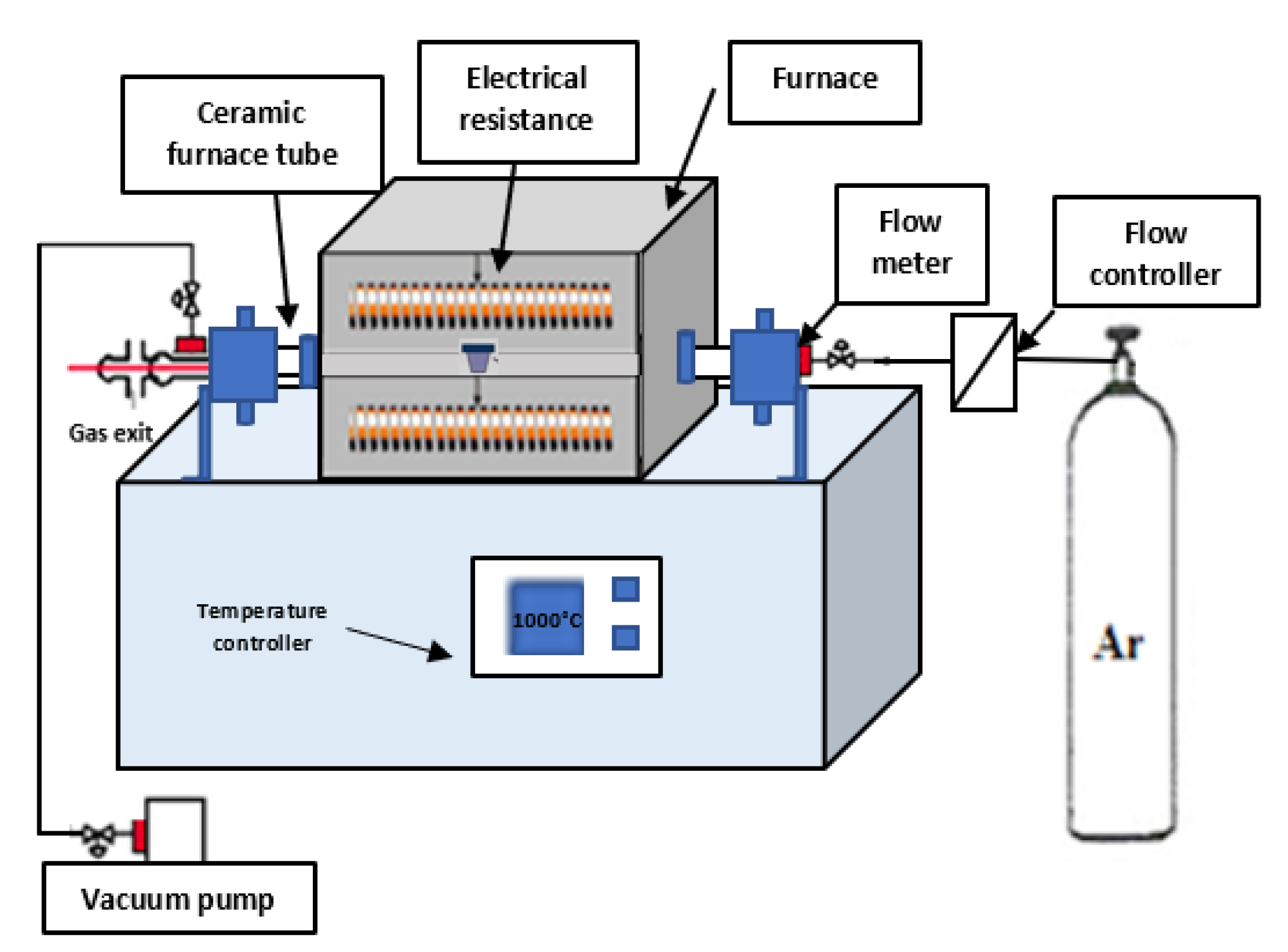
2. Materials and Methods

The purpose of this work is the determination of the most suitable conditions for producing samples with satisfactory properties and simultaneously minimizing the cost and production time. For the deposition process, a two-step pack cementation process consisting of a chromizing (first step—several chromium silicides phases) and a siliconizing step (second step—CrSi2 phase) was applied. In detail, (100) oriented Si substrate was cut into pieces and then carefully cleaned with alcohol. During the chromizing step, the prepared substrates were placed in porcelain crucibles, filled with a powder mixture composed of chromium (99.9%, ~325 mesh), which is the donor material, a halide activator (NH4Cl), and an inert filler (Al2O3). It should be noticed that the inert filler was not mixed with the rest of the powders. The alumina was placed at the top and bottom of the crucible to fill the empty space. The crucibles were sealed with ceramic lids and placed in a tubular electric furnace, which was argon-purged (99.998% Ar gas; Figure 1). After the heat treatment period, the crucibles were left in the furnace to cool down to ambient temperature without interrupting the Ar flow. All of the formed samples were cleaned with an ultrasonic bath machine to enhance the removal of foreign substances from the surface of the samples submerged in an ultrasonically activated liquid.
Several experiments were performed at various heating temperatures from 800 °C to 1150 °C for 120 min and different deposition times, 15, 30, 60, 120 min at a constant temperature of 1000 °C in the chromizing step (Table 1). In all cases, a pack mixture with a Cr content of 40 wt.% Cr was used. The Cr concentration was selected due to the successful formation of Cr–Si compounds in our previous work [22]. The treatment time did not include the time it took for the specimens to cool from the deposition temperature to room temperature.
The higher chromium silicide was the subject of numerous investigations, mainly because of its good oxidation resistance, semiconducting properties at elevated temperatures, and thermoelectric properties. For this reason, a second step of the pack cementation process (siliconizing step) was performed for selective samples synthesized under various heating temperatures and deposition times in the chromizing step. In this case, the pack mixture includes 15 wt.% Si (donor material), 3 wt.% NH4Cl (activator) and 82 wt. % inert Al2O3 (filler). The depositions were performed at 1050 °C for 60 min.
Thermodynamic predictions were performed using the Thermocalc computer program with SSUB4 database Scientific Group Thermodata Europe to present some preliminary results about the Cr–Si compounds formed during the pack cementation process. It was assumed that the pack cementation process occurred at atmospheric pressure and the temperature was homogenous throughout. An inert Ar atmosphere was also assumed. Since Al2O3 is not expected to react or decompose, the existence of the inert filler will not be considered in the calculations. No oxygen-containing solid or gaseous phases were included in the calculations. For the calculation, the presence of the Si substrate was taken into consideration, while the input parameters for the program were fixed based on 10 gr of a pack containing 40 wt.% Cr, 57 wt.% filler (Al2O3), and 3 wt.% halide activator salt (NH4Cl). It should be noticed that these thermodynamic approximations are for an equilibrium state, and thus, the experimental results may vary, and different phases may be formed.
Scanning Electron Microscopy (SEM) was used to examine the morphology and the chemical composition of the samples using a 20 kV JEOL 840A SEM equipped with an OXFORD INCA 300 Energy Dispersive X-ray Spectroscopy (EDS) analyzer (Jeol Ltd., Akishima, Tokyo, Japan). X-ray powder diffraction graphs (XRD) were recorded at Bragg–Brentano (BB) geometry using a two-cycle Rigaku Ultima+ powder X-ray diffractometer (Rigaku Corporation, Shibuya-Ku, Tokyo, Japan) with a Cu Ka radiation operating at 40 kV/30 mA). Finally, thermogravimetric (TGA) measurements were used to examine the thermal stability of CrSi2 samples, which were performed with a TG-DTA SETARAM SETSYS 16/18 (Setaram Instrumentation, Caluire, France). The samples were heated from room temperature up to 1000 °C at a heating rate of 10 °C/min and air flow about 50 mL/min. Τhe samples were cut to a suitable size to fit inside the crucible, polished, and then cleaned. The surface area was calculated in each case (mm2). The mass samples were in the range of 20–35 mg. The samples in bulk form (expressed in mg/mm2) were put in alumina crucibles, with an empty alumina crucible used as a reference; sample temperature and weight were continuously recorded to obtain in situ quantitative data relating to the rate of oxidation of the samples.

3. Results and Discussion

3.1. Thermodynamic Prediction of Pack Compounds Formed

Pack Cementation is an in situ chemical vapor deposition process that comprises two steps, the thermochemical reactions, and the solid-state diffusion. In the case of the Cr–Si system, during the first part, the Cr donor powder reacts with the activator (NH4Cl), which primarily is transformed from α-NH4Cl phase to β-NH4Cl [21]. Then, it decomposes above 200 °C [21,22,25], forming HCl vapors that react with the Cr powder. The as-formed gaseous chlorides decompose on the substrate (vapor transport to the substrate surface occurs because of the high thermodynamic activity in the powder mixture and the low activity at the substrate surface [26]), resulting in the deposition of the donor material in a highly reactive form (via the formation of chlorides) that promotes metal–metal interaction. According to the literature [26], at the surface, the transportation of the desired element occurs via several possible deposition reactions such as the disproportionation, displacement reaction with the substrate, and reaction with the environment. Additionally, the byproducts of the reaction react again with the donor material and the process is repeated until the donor is fully consumed. This method has also been reported in the literature and it happens without requiring high vacuum conditions, unlike other methods [26,27,28]. Eremenko et al. [14] have studied the Cr–Si system and measured the Gibbs energies of Cr silicides as a function of temperature at various temperatures from 700 to 850 °C. They found that the gas partial pressure of Cr chlorides is sufficiently high to transfer a part via the gas phase to the silicon surface. Therefore, the deposition of Cr in a more reactive form is mainly attributed to the decomposition of the activator and the reaction of the products with the Cr powder and the Si substrate. From this stage, a thermal diffusion process occurs by Si atoms to be the predominant species. Several marker techniques were developed during the past few years to determine the dominant diffusing species during the solid-state interaction between thin metal films and Si to form silicides. For the deposition of Cr on Si substrate, several marker studies were performed by using Xe and radioactive 31Si. It was found that the diffused species are the Si atoms [5,25,29]. Additionally, Si atoms are the element with the lowest melting point and the bigger total interfacial area, which will diffuse faster in order to reduce the free energy of the system [30,31,32].
The Thermocalc computing program was used to present some preliminary results about the Cr–Si phases that are thermodynamical to be formed under the pack cementation process. Figure 2 shows the phases that are thermodynamically stable and hence are likely to be formed for a pack containing 40 wt.% Cr and 3 wt.% NH4Cl activator at 1000 °C as a function of the Si amount. Since the amount of Si increases, new phases will appear. Therefore, the Cr3Si is the first thermodynamically phase formed, followed by the Cr5Si3, CrSi, and CrSi2. The CrSi2 phase becomes increasingly stable as the amount of Si increases. According to the phase diagram of the Cr–Si system [5] and knowing that the elemental ratio of CrSi2 is 1:2, this phase may appear as we move away from the surface of the coating. Therefore, moving from the surface inwards, the stable phases appear to be: Cr3Si, Cr5Si3, CrSi, and CrSi2. As mentioned above, this trend is expected because Si atoms disperse more quickly [25,29]. However, it should be noticed that the phases on the substrate will be determined by the element deposited, phase diagram, and interdiffusion kinetics.

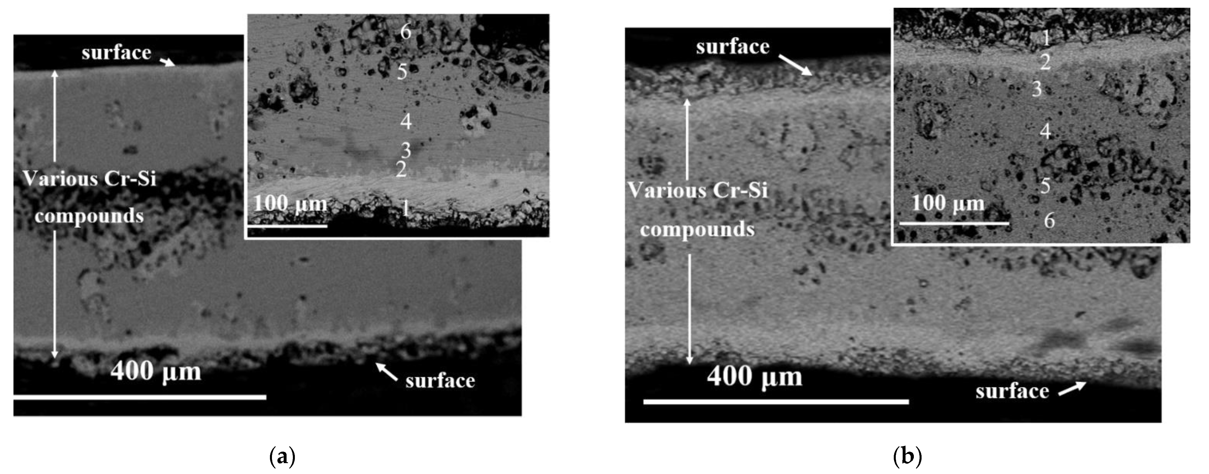
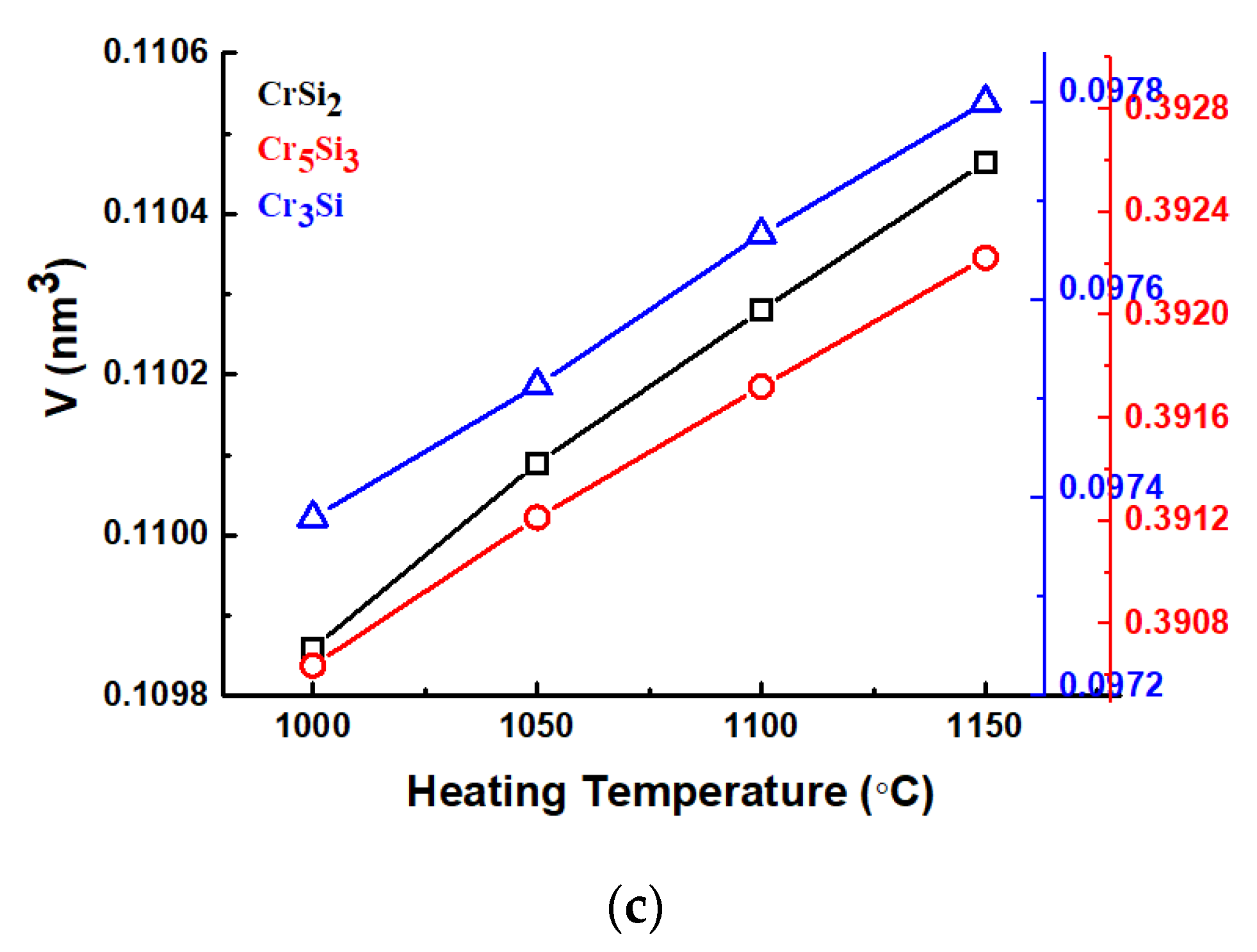
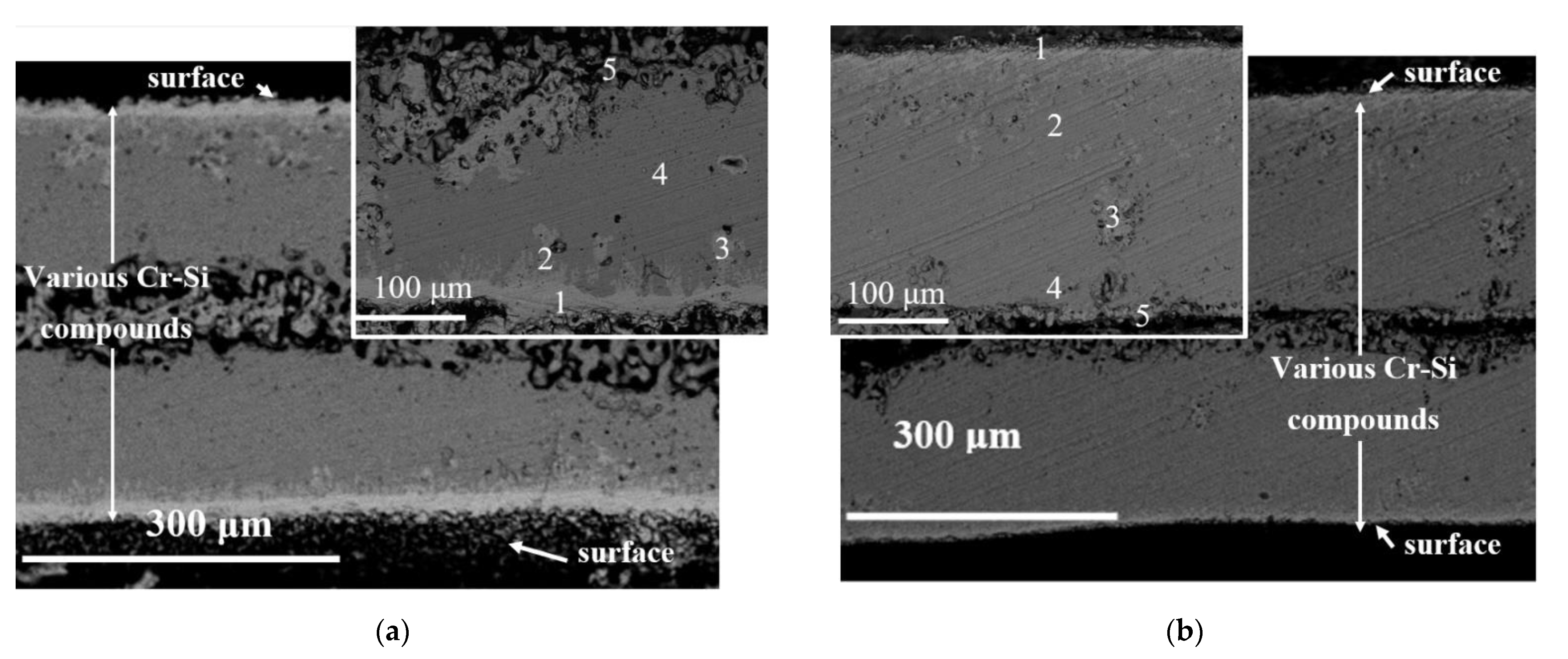
3.2. Effect of Deposition Temperature

Chromium silicides compounds were synthesized by pack cementation process for 40 wt.% Cr, 3 wt.% NH4Cl, and 57 wt.% Al2O3 in the pack mixture at various temperatures. The coating quality formed at temperatures below 1000 °C is very poor. The coating thickness is inhomogeneous, large areas of the silicon substrate are exposed and there are many cracks and cavities. Additionally, inclusions of alumina were being observed in the coating originating from the powders of the pack mixture due to the outward diffusion [30,31]. For this reason, the inert filler was not mixed with the Cr powder and NH4Cl activator; it was placed at the top and bottom of the crucible to fill the space, as described in the experimental section. Since coatings of that quality are useless for any kind of application, we will focus on the samples formed at 1000 °C to 1150 °C. Figure 3 shows some typical SEM cross-section micrographs (at different magnifications) of the samples formed during the chromizing step at various temperatures. According to the cross-sectional SEM micrographs, the micrograph is “divided” into two parts. This is because a full transformation of the Si substrate into various chromium silicide compounds occurs, forming cracks and holes. The consumption of Si substrate for the formation of Cr–Si compounds, and the faster diffusion of Si leads to cracks and voids, which are formed due to the difference in intrinsic diffusivities of chemical constituents (higher Si diffusion rate compared to Cr) named the Kirkendall effect [32]. The cracks might have also been caused by the thermal expansion coefficient mismatch between the formed compounds and the substrate.
EDS analysis was performed on several regions of the samples to identify the as-formed structure. Table 2 presents the cross-sectional EDS analysis of the chromized samples obtained by use of 40 wt.% Cr in the pack mixture for 120 min at 1000 °C, 1050 °C, 1100 °C, and 1150 °C. In Figure 3, areas denoted as #1 and #2 were found to contain Cr-rich compounds, while the EDS analysis of #4, #5, and #6 shows compounds that are rich in Si. This is expected from the Thermocalc calculations about equilibrium phases formed during pack cementation. It seems that Si-rich and Cr-rich phases were formed near the consumed substrate and the surface, respectively, during the chromizing step.
Figure 4 shows the XRD pattern of the samples synthesized with 40 wt.% Cr in the pack mixture at various heating temperatures. In Figure 3, areas #1-#2 and #4-#6 correspond to Cr5Si3 and CrSi2 phases, respectively, based on the results of EDS analysis in Table 2 and XRD characterization. The areas denoted as #2, #3 in the 1000_120 min, #3 in 1050_120 min, #2 in 1100_120 min and #3, #5 in 1150_120 min samples correspond to the CrSi phase. The results of EDS analysis for all samples agree with the identification of the XRD patterns, indicating that the same compounds were found in the diffraction patterns of all samples synthesized between 1000 and 1150 °C. Once again, it is apparent that phases ‘rich’ in Cr appear near the surface of the samples, while phases ‘rich’ in Si are in the center of samples. This is also confirmed by the thermodynamic calculations in Figure 2 and the literature results [22].
Figure 5 shows the lattice parameters (a and c) and the cell volume (v) versus temperature for CrSi2, Cr3Si, and Cr5Si3 calculated by the Rietveld refinement. The errors are estimated to be generally lower than 9 × 10⁻⁵ and 3 × 10⁻⁵ for the α and c lattice parameters, respectively. The lattice parameters (a and c) and the cell volume (v) versus temperature for CrSi2, Cr3Si, and Cr5Si3 slightly increase with increasing the heating temperature. After the formation of a silicide compound, the layer grows either by metal atom motion at the silicon–silicide interface or by silicon atom motion at the silicide–metal interface. As discussed above, the diffusion process of Si on the silicide compounds of Cr is very fast under these conditions. Although the movement of Si atoms does not cause significant stresses, once they have arrived at their respective interfaces, the Si atoms will react with chromium to form Cr–Si silicides. This process causes an increase in volume. Additionally, the c/a ratio for CrSi2 was found to be ~1.43 deviating from the ideal value of 1.5 [33]. Dasgupta et al. [8] have found a value of 1.438 for the c/a ratio of CrSi2 supporting that this deviation results in smaller interlayer bond distances.
The thermal expansion coefficients (α) were calculated by using the data of the lattice parameters [35,36]. In the temperature range studied (1000–1150 °C), the thermal expansion coefficients were found to be αα = 9.64 × 10⁻⁶ °C−1 and αv = 28.93 × 10⁻⁶ °C−1 for Cr3Si; αα = 6.41 × 10⁻⁶ °C−1, αc = 14.07 × 10⁻⁶ °C−1 and αv = 26.89 × 10⁻⁶ °C−1 for Cr5Si3 and αα = 11.77 × 10⁶ °C1, αc = 17.72 × 10⁻⁶ °C−1 and αv = 36.30 × 10⁻⁶ °C−1 for CrSi2. These results confirm the relationship between linear and volumetric thermal expansion coefficients (αv = 3αl) for the Cr3Si cubic system and are in good agreement with the literature results [36]. The thermal expansion coefficients of Cr5Si3 and CrSi2 present anisotropy between the two crystallographic axes. The results for the thermal expansion coefficients of Cr5Si3 and CrSi2 were compared with the literature and were found to be in good agreement [8,36,37,38]. According to the literature [37,39], the thermal expansion coefficients are isotropic for cubic materials, but it is expected to be anisotropic in non-cubic material such as orthorhombic disilicides and hexagonal 5–3 silicides. Additionally, it is known that the thermal expansion coefficient in the c-direction is larger than that in α-direction for most compounds due to the complex crystal structure and the different bond strength along with different crystal orientations [40]. The different values of thermal expansion coefficients between the formed compounds and the substrate (the coefficient of expansion for Si is 2.6 × 10⁻⁶ °C−1) lead to anisotropy which can cause micro-cracks during the procedure.

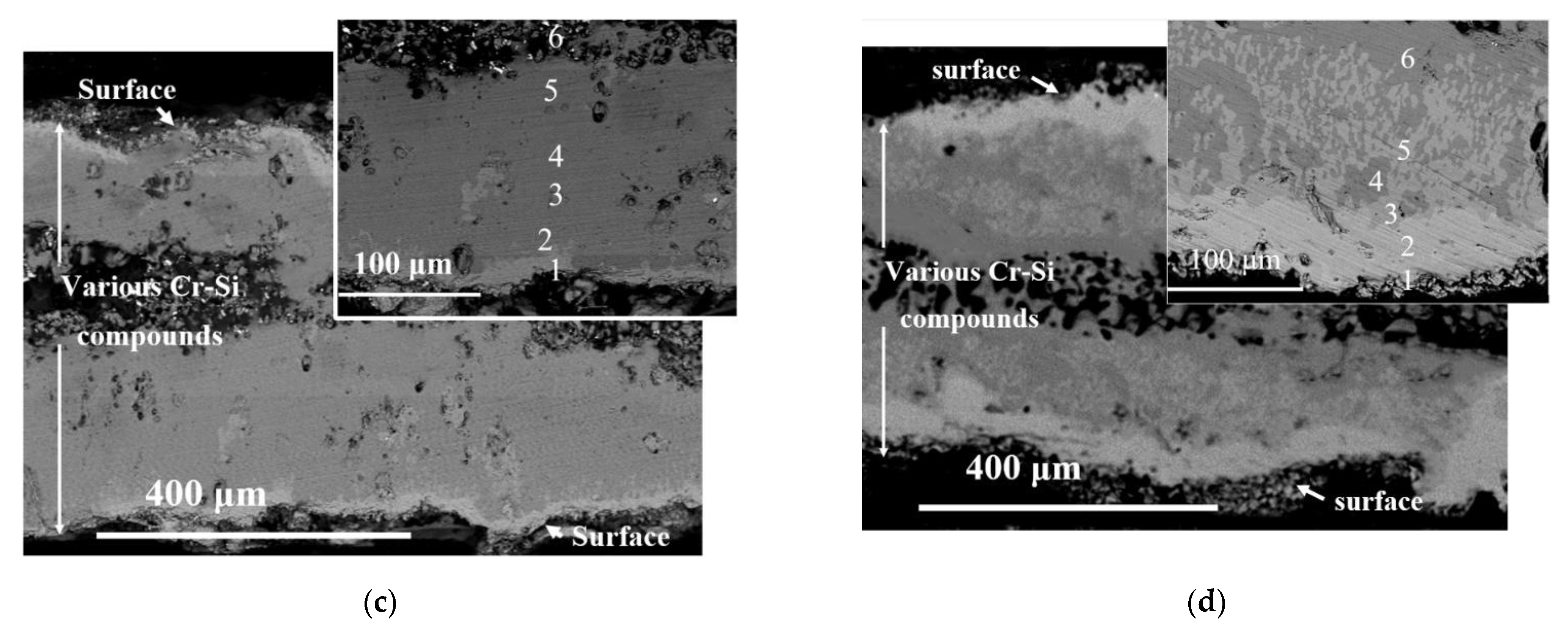
3.3. Effect of Deposition Time

Then, experiments for chromium silicides were performed at 1000 °C for various deposition times ranging from 15 to 120 min. Figure 6 shows cross-sectional SEM micrographs (at different magnifications) of chromizing samples for various times. On the one hand, the four samples do not present considerable differences in the silicides formed because both the longer and shorter heating times have led to the formation of all chromium silicide compounds. It should be mentioned again that a full transformation of the Si substrate into chromium silicide compounds can be seen in Figure 6. Table 3 presents the cross-sectional EDS analysis of the chromized samples obtained by use of 40 wt.% Cr in the pack mixture for 120 min, 60 min, 30 min, and 15 min at 1000 °C. Once again, from the results of EDS analysis, it seems that Cr-rich and Si-rich phases were formed near the surface and consumed substrate of samples, respectively. On the other hand, the heating time variations seem to affect the thickness of the samples, which increases with the increase in the deposition time. The cross-sectional SEM micrographs of the samples synthesized at shorter times appear to be more homogeneous compared to the longer ones without presenting large cracks and cavities. For longer deposition time (120 min), the CrSi2 and CrSi compounds, that are formed first after the transformation of Si substrate into chromium silicides, are consumed to form Cr-rich phases due to the fast Si diffusion leading to a large density of cracks and holes. According to the literature [16], after consuming all the available silicon, CrSi2 can react with unconsumed chromium to form Cr5Si3 or Cr3Si.
Figure 7 shows the typical XRD diagrams of the chromizing samples for various deposition times. According to the XRD characterization and cross-sectional SEM micrographs, various chromium silicide phases such as CrSi2, CrSi, CrSi3, and Cr5Si3 are formed for all the synthesized samples. Therefore, even at the lowest deposition time of 15 min, a full transformation of the Si wafer into chromium silicide compounds occurs (Figure 6d) because of the very rapid diffusion of silicon in the Cr–Si compounds.
According to SEM micrographs, it is obvious that the thickness increases with time. Figure 8 shows the dependence of the thickness as a function of time. There is a nearly parabolic relationship between the thickness of the silicides formed and the deposition time in agreement with the literature results [41]. The growth of chromium silicides follows a uniform process with the layer-by-layer diffusion of silicon in the early stages. The Si diffusion becomes easier from the substrate through the first formed chromium silicide phase in the regions where Cr has not yet reacted. However, cracks and porosity are formed due to the fast diffusion of Si atoms and the different values of thermal expansion coefficients between the Si substrate and the formed Cr–Si compounds leading to strong morphological abnormalities. As mentioned earlier, a larger number of cracks and holes appeared in the sample synthesized at 1000_120 min compared to that synthesized at a shorter deposition time. It should be noted that an increase in the sample thickness is not always the result of growth under isothermal conditions (deposition time selected). Some layers may be developed during cooling from elevated temperatures to room temperature.

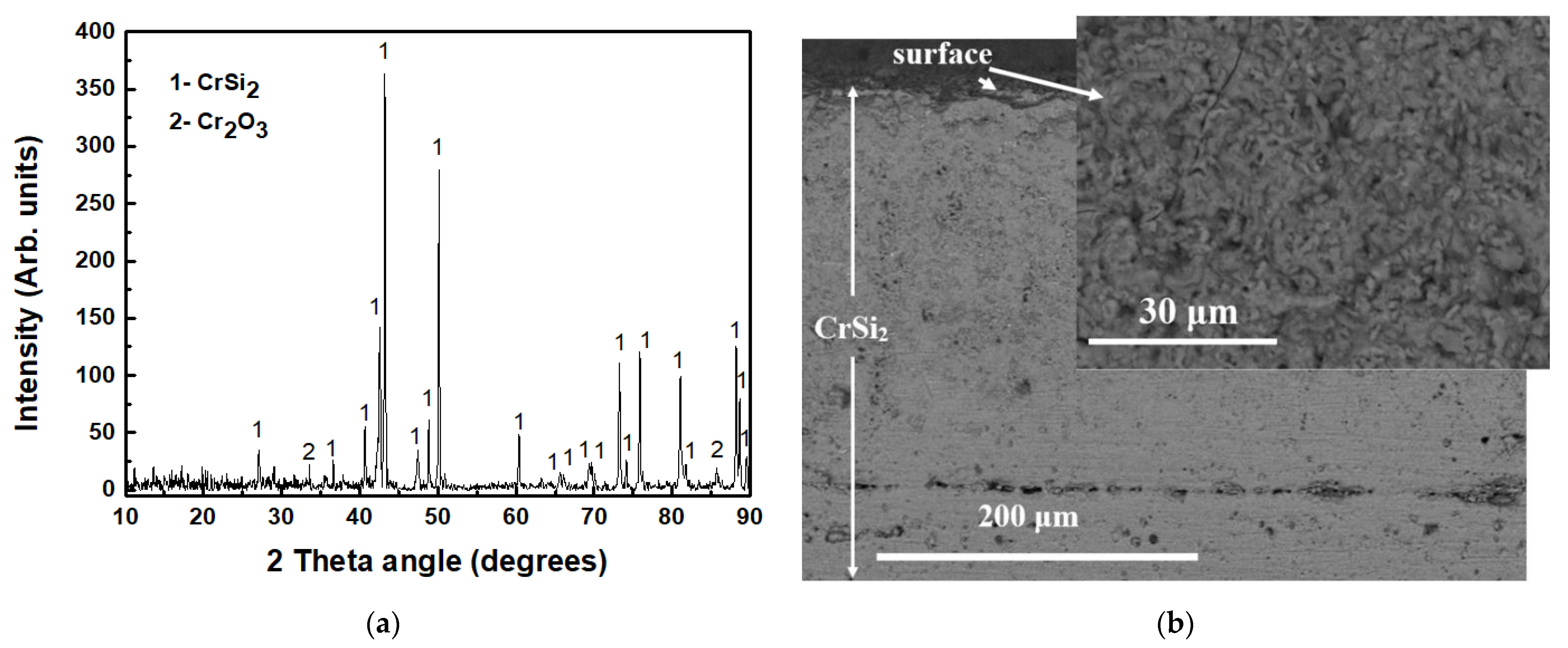
3.4. Siliconizing Step

The higher chromium silicide (CrSi2 phase) was the subject of numerous investigations, mainly because of its good oxidation resistance, semiconducting properties at elevated temperatures, and thermoelectric properties [22,41,42,43,44]. According to the pack chromizing results, several Cr the sample synthesized at 1000_120 min Si compounds were formed, the majority of which are rich in Cr. To enrich the Cr-Si compounds with Si, the second step of pack cementation process was performed by using Si powder as the donor material. Figure 9 shows the typical cross-sectional and plan-view SEM micrographs (shown inset) of selective siliconized CrSi2 samples. EDS analyses at several areas of cross-sectional and plan-view micrographs revealed that the elemental ratio of Cr: Si was 1:2 (34 ± 3 at.% Cr and 63 ± 3 at.% Si). No other chromium silicide phases or impurities were found. The cross-sectional SEM micrographs of selective samples present gaps and holes that pre-existed in the first chromizing step (Figure 3 and Figure 6). However, the 1000_15 min sample in Figure 9d, synthesized at 1000 °C for 15 min during the chromizing step, seems to be more homogeneous with smaller cracks and holes compared with those synthesized at higher temperatures and longer times. Additionally, for the plan-view SEM micrographs, the surface morphology of 1000_15 min is quite homogeneous with some porosities in places, as shown inset in Figure 9d. For the same temperature but after 120 min, the surface morphology is dense and present elevated roughness with distinguishable low depth craters, while the morphology of the higher heating temperature samples also looks more uniform, and smoother compared to that of 1000_120 min sample. The atoms obtain higher energy decreasing the crystalline defects densities and forming smooth surfaces [45,46].
The XRD results in Figure 10a show the presence of the CrSi2 compound indicating that the previously Cr phases were successfully enriched with Si. It should be mentioned that very sharp and high peaks of the CrSi2 phase appear for all the examined samples. The various chromium silicide phases could not prevent the fast Si diffusion into the substrate (now, the substrate is the various chromium compounds synthesized in the chromizing step), and thus, the CrSi2 phase is formed. Table 4 presents the thickness of the samples synthesized at 1000_120 min, 1150_120 min, and 1000_15 min, which gradually increases from approximately 540 μm to 620 μm and 611 μm, respectively. The thickness increases with increasing the heating temperature and decreasing the deposition time in the chromizing step. Therefore, the most noticeable evolution in thickness is observed for 1150_120 min and 1000_15 min samples. However, as discussed above, the deposition time of 120 min is long enough to consume all the Si substrate due to the fast Si diffusion, leading to the formation of a large number of cracks.
The crystallite size was calculated by using Williamson–Hall (W–H) analysis [47]. The crystalline size was estimated from the y-intercept of the linear fit to the data of a plot of 4sinθ along the x-axis and wcosθ along the y-axis. Figure 10b shows the crystalline size of the synthesized CrSi2 samples in the siliconizing step. It was found to change from 43.14 nm to 76.62 nm and 26.24 nm for 1150_120 min, 1000_120 min, and 1000_15 min, respectively, in agreement with the literature results for the crystallite size of the CrSi2 samples [21,42].
For the examination of the thermal stability of the CrSi2 samples, TGA experiments were performed in an air environment by heating the samples under non-isothermal conditions from room temperature up to 1000 °C. Τhese experiments look at whether the materials could work properly without being degraded by oxides. Τhe main emphasis is given on how the different synthesis conditions have influenced the material’s thermal stability. Figure 11 shows the mass gain per unit area curves for CrSi2 samples synthesized at various temperatures and times. Τhe samples present high thermal stability because the increase in mass up to 1000 °C is insignificant compared with the total mass before oxidation. It can be seen that the mass gain per unit area is even lower than 0.006 mg/mm2. This can be explained by the high diffusivity of Cr in the nanostructure and the active formation of a Cr-rich oxide layer [48,49]. According to the literature [50], the oxidation rate of CrSi2 is determined by the diffusion of all the reaction components at lower temperatures (700–900 °C), whereas it is mainly controlled by the diffusion of chromium over cationic vacancies in the p-type Cr2O3 lattice at higher temperatures.
Table 4 presents the critical temperature at which the oxidation rate becomes significant. The oxidation starts at about 505 °C and 609 °C for the 1150_120 min and 1000_15 min samples, respectively. The samples synthesized at a higher temperature and a shorter time appear to increase start-up oxidation temperatures. However, surface roughness was shown to play a role in the oxidation behavior of several materials [51,52,53,54,55,56]. Platt et al. [54] reported that there is a clear trend towards rougher surfaces generating thicker oxides. Charpentier et al. [53] found that a rougher initial surface favors the hardness of the oxide layer, which could be correlated to a better adherence between the oxide layer and the substrate. In our case, the 1000_15 min sample was found to present the lower surface roughness (Figure 9d) compared with that synthesized at longer deposition times and higher temperatures. It seems that the initial surface roughness affects the oxidation rate; the largest surface roughness provides the largest mass gain per unit area. Additionally, the 1000_15 min CrSi2 sample has the lowest crystallite size. It was reported that materials with nanocrystalline size affect thermal stability [57,58,59,60]. Birbilis et al. [59] showed that nanocrystalline materials with fine grain size and high diffusion coefficients facilitate the formation of protective oxides. In our previous work [21], the crystallite size for CrSi2 in powder form (32.5 nm) was calculated; the compound was found to be stable up to 690 °C, forming a protective layer of chromium and silicon oxides.
Bulk CrSi2 was found to be stable in the air up to 700 °C due to the formation of a protective layer of Cr2O3 or SiO2, limiting the oxygen diffusion [48]. The XRD patterns of the oxidized samples after TGA tests confirm the presence of a small amount of Cr2O3 in Figure 12a. However, it should be mentioned that, in the XRD pattern, the CrSi2 is still the dominant phase after the thermal oxidation tests of all studied materials. No Si oxides can be found in the XRD pattern because of their small amount or concurrence of their most intense peaks with peaks of other present compounds or the presence of amorphous SiO2. This result is in good agreement with the literature data [48], showing that Cr2O3 is the only oxide phase detected in the diffraction patterns at 1000 °C. It was reported that the Cr2O3 is a thermodynamically stable phase up to high temperatures due to its high melting point, forming an adherent layer that reduces oxygen interaction [61].
The non-isothermally oxidized CrSi2 samples were also examined with SEM microscopy and EDS analysis. Figure 12b shows the selected cross-sectional SEM micrograph and the corresponding plan-view image (shown in inset) for the siliconizing sample synthesized at 1000_120 min in the chromizing step. From the EDS analysis, the non-isothermally oxidized CrSi2 samples were found to contain 62.3 (±2.25) at.% Si and 30.9 (±2.30) at.% Cr. Once again, the EDS analyses reveal that the CrSi2 is the dominant phase after thermal oxidation tests confirming the thermal stability of the synthesized samples. The oxide scale compounds which were formed in the material are at an insignificant concentration.

4. Conclusions

This study reports the synthesis of chromium silicide phases by the pack cementation process studying the effect of the deposition time t and the heating temperature T on the morphology and structure of the synthesized samples. A series of experiments were carried out at temperatures from 1000 to 1150 °C with different deposition times ranging between 15 and 120 min. The effect of different experimental conditions on the structure, composition, and short-term thermal stability in the air was investigated. According to the pack cementation process, the activator is decomposed and reacts with Cr powder and Si substrate. The results of the thermodynamic calculations clearly show that all the equilibrium phases predicted by the Cr–Si phase diagram can be formed during the pack cementation process. XRD patterns revealed the presence of various chromium silicide compounds in all chromizing step cases, without any oxide traces. The deposition temperature and heating time were found to affect the coating thickness and the microstructure of the synthesized samples. All the siliconized samples demonstrated significant thermal stability under non-isothermal measurements in the air. We can conclude that the sample, synthesized at 1000 °C_15 min during the chromizing step in combination with the siliconizing step at 1000 °C for 60 min, presents the best thermal stability. The selected temperatures provide acceptable, economical, and repeatable results. Therefore, pack cementation is a cost-effective and large-scale method to produce chromium silicides.

Author Contributions

Conceptualization, G.V., K.C. and E.T.; methodology, E.T., D.S. and S.A.T.; software, E.T. and S.A.T.; validation, D.S. and E.T.; formal analysis, E.T. and S.A.T.; investigation, E.T.; resources, G.V. and E.T.; data curation, E.T.; writing—original draft preparation, E.T.; writing—review and editing, E.T., G.V. and K.C.; visualization, E.T.; supervision, G.V.; project administration, E.T. All authors have read and agreed to the published version of the manuscript.

Funding

This research received no external funding.

Institutional Review Board Statement

Not applicable.

Informed Consent Statement

Not applicable.

Data Availability Statement

The authors declare that the data presented in this work are available within the article.

Acknowledgments

The authors would like to acknowledge Dimitrios Chaliampalias and E. Pavlidou of the Physics Department, Aristotle University of Thessaloniki for their support.

Conflicts of Interest

The authors declare no conflict of interest.

References

  1. Ma, J.; Gu, Y.; Shi, L.; Chen, L.; Yang, Z.; Qian, Y. Synthesis and Thermal Stability of Nanocrystalline Chromium Disilicide. J. Alloy Compd. 2004, 376, 176–179. [Google Scholar] [CrossRef]
  2. Tam, P.L.; Cao, Y.; Nyborg, L. XRD and XPS Characterisation of Transition Metal Silicide Thin Films. Surf. Sci. 2012, 606, 329–336. [Google Scholar] [CrossRef]
  3. Tam, P.L.; Cao, Y.; Nyborg, L. Thin Film Characterisation of Chromium Disilicide. Surf. Sci. 2013, 609, 152–156. [Google Scholar] [CrossRef]
  4. Khalil, M.; Moll, A.; Godfroy, M.; Letrouit-Lebranchu, A.; Villeroy, B.; Alleno, E.; Viennois, R.; Beaudhuin, M. Thermoelectric Properties and Stability of Nanostructured Chromium Disilicide CrSi2. J. Appl. Phys. 2019, 13, 126–132. [Google Scholar] [CrossRef]
  5. Gokhale, A.B.; Abbaschian, G.J. The Cr-Si (Chromium-Silicon) System. J. Phase Equilib. 1987, 8, 474–484. [Google Scholar] [CrossRef]
  6. Yin, Y.X.; Wang, H.M. Microstructure and Wear Resistance of Cuss-Toughened Cr5Si3/CrSi Metal Silicide Alloys. J. Mater. Res. 2005, 20, 1122–1130. [Google Scholar] [CrossRef]
  7. Gokhale, A.B.; Abbaschian, G.J.; Filonov, A.B.; Tralle, I.E.; Dorozhkin, N.N.; Migsas, D.B.; Shaposhnikov, V.L.; Petrov, G.V.; Anishchik, V.M.; Borisenko, V.E. Semiconducting Properties of Hexagonal Chromium, Molybdenum, and Tungsten Disilicides. Phys. Status Solidi (B) 1987, 186, 209–215. [Google Scholar]
  8. Dasgupta, T.; Etourneau, J.; Chevalier, B.; Matar, S.F.; Umarji, A.M. Structural Thermal and Electrical Properties of CrSi2. J. Appl. Phys. 2008, 103, 113516. [Google Scholar] [CrossRef]
  9. Vantomme, A.; Nicolet, M.A.; Long, R.G.; Mahan, J.E.; Pool, F.S. Reactive Deposition Epitaxy of CrSi2. Appl. Surf. Sci. 1993, 73, 146–152. [Google Scholar] [CrossRef]
  10. Heck, C.; Kusaka, M.; Hirai, M.; Iwami, M.; Yokota, Y. Thin Film Silicon Compound Growth Mechanisms: CrSi2/Si(001). Thin Solid Film. 1996, 281–282, 94–97. [Google Scholar] [CrossRef]
  11. Solomkin, F.Y.; Zaitsev, V.K.; Kartenko, N.F.; Kolosova, A.S.; Burkov, A.T.; Uryupin, O.N.; Shabaldin, A.A. Structure and Thermoelectric Properties of CrSi2 Crystallized from a Tin Solution-Melt. Tech. Phys. 2010, 55, 750–752. [Google Scholar] [CrossRef]
  12. Shinoda, D.; Asanabe, S.; Sasaki, Y. Semiconducting Properties of Chromium Disilicide. J. Phys. Soc. Jpn. 1964, 19, 269–272. [Google Scholar] [CrossRef]
  13. Nishida, I. The Crystal Growth and Thermoelectric Properties of Chromium Disilicide. J. Mater. Sci. 1972, 7, 1119–1124. [Google Scholar] [CrossRef]
  14. Zhang, D.L. The Sequence of Phase Formation during Mechanical Alloying of Chromium and Silicon Powders. J. Mater. Sci. 1996, 31, 895–899. [Google Scholar] [CrossRef]
  15. Fernandes, B.B.; Rodrigues, G.; Coelho, G.C.; Ramos, A.S. On Iron Contamination in Mechanically Alloyed Cr-Si Powders. Mater. Sci. Eng. A 2005, 405, 135–139. [Google Scholar] [CrossRef]
  16. Colgan, E.G.; Tsaur, B.Y.; Mayer, J.W. Phase Formation in Cr-Si Thin-Film Interactions. Appl. Phys. Lett. 1980, 37, 938–940. [Google Scholar] [CrossRef]
  17. Majumdar, S.; Sengupta, P.; Kale, G.B.; Sharma, I.G. Development of Multilayer Oxidation Resistant Coatings on Niobium and Tantalum. Surf. Coat. Technol. 2006, 200, 3713–3718. [Google Scholar] [CrossRef]
  18. Xiang, Z.D.; Datta, P.K. Relationship between Pack Chemistry and Aluminide Coating Formation for Low-Temperature Aluminisation of Alloy Steels. Acta Mater. 2006, 54, 4453–4463. [Google Scholar] [CrossRef]
  19. Teknetzi, A.; Tarani, E.; Symeou, E.; Karfaridis, K.; Stathokostopoulos, D.; Pavlidou, E.; Kyratsi, T.; Hatzikraniotis, E.; Chrissafis, K.; Vourlias, D. Structure and thermoelectric properties of higher manganese silicides synthesized by pack cementation. Ceram. Int. 2021, 47, 243–251. [Google Scholar] [CrossRef]
  20. Vourlias, G.; Pistofidis, N.; Chrissafis, K.; Pavlidou, E.; Stergioudis, G. Mechanism and Kinetics of the Formation of Zinc Pack Coatings. J. Therm. Anal. Calorim. 2008, 91, 497–501. [Google Scholar] [CrossRef]
  21. Tarani, E.; Chaliampalias, D.; Pavlidou, E.; Chrissafis, K.; Vourlias, G. Thermal Oxidation Kinetics of CrSi2 Powder Synthesized by Pack Cementation Process. J. Therm. Anal. Calorim. 2016, 125, 111–120. [Google Scholar] [CrossRef]
  22. Stathokostopoulos, D.; Chaliampalias, D.; Tarani, E.; Theodorakakos, A.; Giannoulatou, V.; Polymeris, G.S.; Pavlidou, E.; Chrissafis, K.; Hatzikraniotis, E.; Paraskevopoulos, K.M.; et al. Formation of the Thermoelectric Candidate Chromium Silicide by Use of a Pack-Cementation Process. J. Electron. Mater. 2014, 43, 3733–3739. [Google Scholar] [CrossRef]
  23. Stathokostopoulos, D.; Chaliampalias, D.; Stefanaki, E.C.; Polymeris, G.; Pavlidou, E.; Chrissafis, K.; Hatzikraniotis, E.; Paraskevopoulos, K.M.; Vourlias, G. Structure, Morphology and Electrical Properties of Mg2Si Layers Deposited by Pack Cementation. Appl. Surf. Sci. 2013, 285, 417–424. [Google Scholar] [CrossRef]
  24. Teknetzi, A.; Tarani, E.; Stathokostopoulos, D.; Karfaridis, D.; Chrissafis, K.; Vourlias, G. High-Temperature Oxidation Resistance and Thermal Stability of Higher Manganese Silicide Powder Synthesized by Pack Cementation. J. Alloy. Compd. 2021, 873, 159842. [Google Scholar] [CrossRef]
  25. Botha, A.P.; Pretorius, R. Co2Si, CrSi2, ZrSi2 and TiSi2 Formation Studied by a Radioactive 31Si Marker Technique. Thin Solid Film. 1982, 93, 127–133. [Google Scholar] [CrossRef]
  26. Levine, S.R.; Caves, R.M. Thermodynamics and Kinetics of Pack Aluminide Coating Formation on IN-100. J. Electrochem. Soc. 1974, 121, 1051–1064. [Google Scholar] [CrossRef] [Green Version]
  27. Bai, C.Y.; Luo, Y.J.; Koo, C.H. Improvement of High Temperature Oxidation and Corrosion Resistance of Superalloy IN-738LC by Pack Cementation. Surf. Coat. Technol. 2004, 183, 74–88. [Google Scholar] [CrossRef]
  28. Genova, V.; Paglia, L.; Pulci, G.; Bartuli, C.; Marra, F. Diffusion Aluminide Coatings for Hot Corrosion and Oxidation Protection of Nickel-Based Superalloys: Effect of Fluoride-Based Activator Salts. Coatings 2021, 11, 412. [Google Scholar] [CrossRef]
  29. Lien, C.D.; Nicolet, M.A. Mathematical Model for a Radioactive Marker in Silicide Formation. J. Appl. Phys. 1984, 55, 4187–4193. [Google Scholar] [CrossRef] [Green Version]
  30. Jayanth, C.S.; Nash, P. Factors Affecting Particle-Coarsening Kinetics and Size Distribution. J. Mater. Sci. 1989, 24, 3041–3052. [Google Scholar] [CrossRef]
  31. Pan, J.; Le, H.; Kucherenko, S.; Yeomans, J.A. A Model for the Sintering of Spherical Particles of Different Sizes by Solid State Diffusion. Acta Mater. 1998, 46, 4671–4690. [Google Scholar] [CrossRef]
  32. d’Heurle, F.M.; Gas, P. Kinetics of Formation of Silicides: A Review. J. Mater. Res. 1986, 1, 205–221. [Google Scholar] [CrossRef]
  33. Mattheiss, L.F. Electronic Structure of CrSi2 and Related Refractory Disilicides. Phys. Rev. B 1991, 43, 12549–12555. [Google Scholar] [CrossRef] [PubMed]
  34. International Centre for Diffraction Data (ICDD) (Formerly Joint Committee on Powder Diffraction Standards—JCPDS). Powder Diffraction File (PDF); ICDD: Newtown, PA, USA, 2003. [Google Scholar]
  35. Ostling, K.; Zaring, C. Thermal properties of TM silicides. In Properties of Metal Silicides, 2nd ed.; Maex, K., Rossum, M., Eds.; INSPEC, The Institution of Electrical Engineers: Leuven, Belgium, 1995; pp. 35–43. [Google Scholar]
  36. Martienssen, W.; Warlimont, H. Springer Handbook of Condensed Matter and Material Data, 1st ed.; Springer: Berlin/Heidelberg, Germany, 2005; p. 491. [Google Scholar]
  37. Engström, I.; Lönnberg, B. Thermal Expansion Studies of the Group IV-VII Transition-Metal Disilicides. J. Appl. Phys. 1988, 63, 4476–4484. [Google Scholar] [CrossRef]
  38. Ochiai, Y.; Kishida, K.; Tanaka, K.; Inui, H. Mechanical Properties of Cr5Si3 with the D8 m Structure. Mater. Res. Soc. Symp. Proc. 2011, 1295, 213–218. [Google Scholar] [CrossRef]
  39. Shah, D.M. MoSi2 and Other Silicides as High Temperature Structural Materials. In Superalloys; Antolovich, S.D., Stusrud, R.W., MacKay, R.A., Anton, D.L., Khan, T., Kissinger, R.D., Klastrom, D.L., Eds.; TMS (The Minerals, Metals & Materials Society): Pittsburgh, PA, USA, 2012; pp. 409–422. [Google Scholar]
  40. Zhang, L.; Wu, J. Thermal Expansion and Elastic Moduli of the Silicide Based Intermetallic Alloys Ti5Si3(X) and Nb5Si3. Scr. Mater. 1997, 38, 307–313. [Google Scholar] [CrossRef]
  41. Lien, C.D.; Nicolet, M.A.; Lau, S.S. Kinetics of Silicides on Si 〈100〉 and Evaporated Silicon Substrates. Thin Solid Film. 1986, 143, 63–72. [Google Scholar] [CrossRef]
  42. Filonenko, O.; Falke, M.; Hortenbach, H.; Henning, A.; Beddies, G.; Hinneberg, H.J. Structure of Thin CrSi2 Films on Si(0 0 1). Appl. Surf. Sci. 2004, 227, 341–348. [Google Scholar] [CrossRef]
  43. Seo, K.; Varadwaj, K.S.K.; Cha, D.; In, J.; Kim, J.; Park, J.; Kim, B. Synthesis and Electrical Properties of Single Crystalline CrSi2 Nanowires. J. Phys. Chem. C 2007, 111, 9072–9076. [Google Scholar] [CrossRef]
  44. Chen, S.; Chen, Y.; Yan, W.; Zhou, S.; Qin, X.; Xiong, W.; Liu, L. Electronic and Magnetic Properties of Bulk and Monolayer CrSi2: A First-Principle Study. Appl. Sci. 2018, 8, 1885. [Google Scholar] [CrossRef] [Green Version]
  45. Hashim, N.H.; Subramani, S.; Devarajan, M.; Ibrahim, A.R. Structural and Surface Characterization of Undoped ZnO and Cu Doped ZnO Using Sol–Gel Spin Coating Method. J. Mater. Sci.: Mater. Electron. 2016, 27, 3520–3530. [Google Scholar] [CrossRef]
  46. Nivedita, L.R.; Haubert, A.; Battu, A.K.; Ramana, C.V. Correlation between Crystal Structure, Surface/Interface Microstructure, and Electrical Properties of Nanocrystalline Niobium Thin Films. Nanomaterials 2020, 10, 1287. [Google Scholar] [CrossRef] [PubMed]
  47. Nakasawa, H.; Takamatsu, T.; Hayashi, K.; Miyazaki, Y. Relationships between Crystallite Size and Thermoelectric Properties of Nano-Structured CrSi2 Prepared by the Reduction-Diffusion and Spark Plasma Sintering Methods. J. Alloy. Compd. 2021, 861, 157967. [Google Scholar] [CrossRef]
  48. Lu, J.; Yang, H.; Liu, B.; Han, J.; Zou, G. Preparation and Physical Properties of Nanosized Semiconducting CrSi2 Powders. Mater. Chem. Phys. 1999, 59, 101–106. [Google Scholar] [CrossRef]
  49. Ma, J.; Gu, Y.; Shi, L.; Chen, L.; Yang, Z.; Qian, Y. Synthesis and Oxidation Behavior of Chromium Silicide (Cr3Si) Nanorods. J. Alloy. Compd. 2004, 375, 249–252. [Google Scholar] [CrossRef]
  50. Godfroy, M.; Khalil, M.; Niebel, C.; Jarrosson, T.; Foix, D.; Flaud, V.; Serein-Spirau, F.; Viennois, R.; Granier, M.; Beaudhuin, M. Transition Metal Silicide Surface Grafting by Multiple Functional Groups and Green Optimization by Mechanochemistry. Phys. Chem. Chem. Phys. 2019, 21, 25720–25727. [Google Scholar] [CrossRef]
  51. Liu, L.; Li, Y.; Wang, F. The Effect of Micro-Structure on the Oxidation Behavior of a Ni-Based Superalloy in Water Vapor plus Oxygen. Mater. Lett. 2008, 62, 4081–4084. [Google Scholar] [CrossRef]
  52. Evans, J.L. Effect of Surface Roughness on the Oxidation Behavior of the Ni-Base Superalloy ME3. J. Mater. Eng. Perform. 2010, 19, 1001–1004. [Google Scholar] [CrossRef]
  53. Charpentier, L.; Lucas, R.; Foucaud, S.; Glénat, H.; Balat-Pichelin, M. Influence of Surface Roughness and Temperature on the Oxidation Behavior of ZrC/SiC Samples. Ceram. Int. 2016, 42, 10985–10991. [Google Scholar] [CrossRef]
  54. Platt, P.; Allen, V.; Fenwick, M.; Gass, M.; Preuss, M. Observation of the Effect of Surface Roughness on the Oxidation of Zircaloy-4. Corros. Sci. 2015, 98, 1–5. [Google Scholar] [CrossRef]
  55. Uran, S.; Veal, B.; Grimsditch, M.; Pearson, J.; Berger, A. Effect of Surface Roughness on Oxidation: Changes in Scale Thickness, Composition, and Residual Stress. Oxid. Met. 2000, 54, 73–85. [Google Scholar] [CrossRef]
  56. Nowak, W.J. Effect of Surface Roughness on Early Stage Oxidation Behavior of Ni-Base Superalloy in 625. Appl. Syst. Innov. 2018, 1, 32. [Google Scholar] [CrossRef] [Green Version]
  57. Mahesh, B.V.; Raman, R.K.S. Role of Nanostructure in Electrochemical Corrosion and High Temperature Oxidation: A Review. Metall. Mater. Trans. A 2014, 45, 5799–5822. [Google Scholar] [CrossRef] [Green Version]
  58. Raman, R.K.S.; Gupta, R.K. Oxidation Resistance of Nanocrystalline Vis-à-Vis Microcrystalline Fe-Cr Alloys. Corros. Sci. 2009, 51, 316–321. [Google Scholar] [CrossRef]
  59. Gupta, R.K.; Birbilis, N.; Zhang, J. Oxidation Resistance of Nanocrystalline Alloys. In Corrosion Resistance, 1st ed.; Shih, H., Ed.; IntechOpen: Rijeka, Croatia, 2012; pp. 213–238. [Google Scholar]
  60. Xia, Z.X.; Zhang, C.; Huang, X.F.; Liu, W.B.; Yang, Z.G. Improve Oxidation Resistance at High Temperature by Nanocrystalline Surface Layer. Sci. Rep. 2015, 5, 1–7. [Google Scholar] [CrossRef] [PubMed]
  61. Stott, F.H.; Wood, G.C.; Stringer, J. The Influence of Alloying Elements on the Development and Maintenance of Protective Scales. Oxid. Met. 1995, 44, 113–145. [Google Scholar] [CrossRef]
Figure 1. A schematic of the experimental growth procedure.
Cmd 02 00012 g001
Figure 2. Amount of equilibrium phases formed during pack cementation process as a function of the Si amount.
Cmd 02 00012 g002
Figure 3. The cross-sectional morphologies at 400 μm and 100 μm (shown inset) of the chromized samples obtained by using 40 wt.% Cr in the pack mixture for 120 min at (a) 1000 °C; (b) 1050 °C; (c) 1100 °C; (d) 1150 °C. The areas denoted as #1, #2, #3, #4, #5, and #6 correspond to the EDS analysis presented in Table 2.
Cmd 02 00012 g003aCmd 02 00012 g003b
Figure 4. XRD pattern of the chromized sample obtained by 40 wt.% Cr in the pack mixture for 120 min at (a) 1000 °C; (b) 1050 °C; (c) 1100 °C; (d) 1150 °C. The peaks were indexed by use of PDF #75-2250 (Cr3Si), #51-1357 (Cr5Si3), #35-0781 (CrSi2), and #51-1356 (CrSi) [34].
Cmd 02 00012 g004
Figure 5. (a,b) Refined lattice parameters; (c) cell volume of CrSi2, Cr3Si, and Cr5Si3 as a function of temperature.
Cmd 02 00012 g005aCmd 02 00012 g005b
Figure 6. The cross-sectional SEM micrographs at 300 μm and 100 μm (shown inset) of the chromized samples, obtained by use of 40 wt.% Cr, deposited at 1000 °C for (a) 120 min; (b) 60 min; (c) 30 min; (d) 15 min. The areas denoted as #1, #2, #3, #4, and #5 correspond to the EDS analysis presented in Table 3.
Cmd 02 00012 g006aCmd 02 00012 g006b
Figure 7. XRD pattern of the chromized sample obtained by use of 40 wt.% Cr in the pack mixture at 1000 °C for (a) 120 min; (b) 60 min; (c) 30 min; (d) 15 min. The peaks were indexed by use of PDF #75-2250 (Cr3Si), #51-1357 (Cr5Si3), #35-0781 (CrSi2) and #51-1356 (CrSi) [34].
Cmd 02 00012 g007
Figure 8. Time dependence of the thickness of the chromized samples deposited at 1000 °C for different deposition times.
Cmd 02 00012 g008
Figure 9. Cross-sectional at 400 μm and the corresponding plan-view SEM micrographs at 100 μm (shown inset) of the siliconized samples obtained by use of 15 wt.% Si in the pack mixture for the sample synthesized during the chromizing step at (a) 1150_120 min; (b) 1000_120 min; (c) 1000_30 min; (d) 1000_15 min.
Cmd 02 00012 g009
Figure 10. (a) XRD pattern of the siliconized samples; (b) crystallite size calculated by the WH analysis. The peaks were indexed by use of PDF #35-0781 (CrSi2) [34].
Cmd 02 00012 g010
Figure 11. TGA non-isothermal curves of the as-formed CrSi2 samples synthesized at various (a) temperatures and (b) times during the chromizing step.
Cmd 02 00012 g011
Figure 12. (a) Bragg–Brentano XRD pattern; (b) SEM micrographs of non-isothermally oxidized CrSi2 samples during non-isothermal oxidation from ambient temperature to 1000 °C. The peaks were indexed by the use of PDF #35-0781 (CrSi2) and #38-1479 (Cr2O3) [34].
Cmd 02 00012 g012
Table 1. Two sub-series of experiments took place during the chromizing step.
1st Set2nd Set
Sample NameHeating Temperature (°C)Sample NameDeposition Time (min)
1000_120 min10001000_120 min120
1050_120 min10501000_60 min60
1100_120 min11001000_30 min30
1150_120 min11501000_15 min15
Table 2. EDS scannings of the chromized samples obtained by 40 wt.% Cr in the pack mixture for 120 min at various temperatures.
A/A1000_120 min1050_120 min1100_120 min1150_ 120 min
Si (at.%)Cr (at.%)Si (at.%)Cr (at.%)Si (at.%)Cr (at.%)Si (at.%)Cr (at.%)
134.74 ± 2.2465.26 ± 2.6738.67 ± 2.5461.33 ± 3.0131.23 ± 3.0168.77 ± 2.5632.63 ± 2.4567.37 ± 2.78
250.75 ± 1.8449.25 ± 1.9636.01 ± 2.4563.99 ± 2.6752.14 ± 1.6947.86 ± 1.8233.16 ± 2.2266.84 ± 2.67
344.77 ± 1.9555.23 ± 1.7147.56 ± 2.5552.44 ± 2.1566.62 ± 1.4533.38 ± 1.2349.53 ± 1.9750.47 ± 1.61
462.44 ± 2.3437.56 ± 1.9861.22 ± 2.8438.78 ± 1.9566.54 ± 1.1133.46 ± 1.2363.81 ± 1.9536.19 ± 1.71
566.78 ± 1.5633.22 ± 1.2665.23 ± 2.0234.77 ± 1.9466.38 ± 1.2133.62 ± 1.1049.91 ± 2.0550.09 ± 1.69
662.72 ± 2.8437.28 ± 1.9466.80 ± 1.3433.20 ± 1.5465.75 ± 1.8734.25 ± 1.7666.75 ± 1.0333.25 ± 1.33
Table 3. EDS scannings of the chromized samples obtained by using 40 wt.% Cr in the pack mixture at 1000 °C for 120 min, 60 min, 30 min, and 15 min.
A/A1000_120 min1000_60 min1000_30 min1000_ 15 min
Si
(at.%)
Cr
(at.%)
Si
(at.%)
Cr
(at.%)
Si
(at.%)
Cr
(at.%)
Si
(at.%)
Cr
(at.%)
122.62 ± 2.4577.38 ± 2.5636.41 ± 2.3363.59 ± 2.1131.89 ± 2.8668.11 ± 2.4531.25 ± 2.7668.75 ± 2.44
248.67 ± 1.9751.33 ± 1.4462.87 ± 2.8937.13 ± 1.8447.65 ± 1.7852.35 ± 1.4345.26 ± 1.8754.74 ± 1.35
354.60 ± 1.0145.40 ± 2.3351.22 ± 1.2148.78 ± 1.6767.43 ± 1.5332.57 ± 1.6462.33 ± 1.7837.67 ± 1.34
465.40 ± 2.0234.60 ± 1.4461.37 ± 2.5438.63 ± 1.7361.09 ± 2.7638.91 ± 1.8061.89 ± 2.9838.11 ± 1.71
564.21 ± 2.5635.79 ± 1.6565.45 ± 1.6733.55 ± 1.2166.64 ± 1.1233.36 ± 1.2165.88 ± 1.4534.12 ± 1.34
Table 4. Calculated parameters from the synthesis of CrSi2 samples at various temperatures and times.
A/ASample NameThickness (μm)Critical Temperature of Oxidation (°C)
11150_120 min620.5504.9
21100_120 min547.9358.9
31000_120 min540.4331.1
41000_60 min567.3344.1
51000_30 min589.4514.4
61000_15 min611.6609.0
Publisher’s Note: MDPI stays neutral with regard to jurisdictional claims in published maps and institutional affiliations.

