1. Introduction
Glasses are the basis for the development of many devices in optical communication, and the possibility to be activated with lanthanide ions allows for the realization of optical amplifiers and light sources [
1,
2]. The advantages in using glasses, and in particular oxide-based dielectric materials, are related to their wide transparency from the ultraviolet to the near-infrared, and good resistance to temperature, corrosion, and radiation [
3,
4,
5]. These features make glass materials particularly convenient for fabricating active optically-confined structures. In the last few years, a lot of effort has been directed in developing appropriate material systems and configurations to exploit and enhance the best luminescence properties of lanthanide ions, such as Er
3+ ions, in photonic glasses [
6,
7]. A possibility for enhancing the emission properties of emitters is given by tailoring their surroundings [
8,
9]. With this aim, several approaches using nanocomposite materials or specific geometries, such as planar interfaces, photonic crystals, solid state planar microcavities, dielectric nanospheres, and spherical microresonators, have been proposed. Moreover, when only Er
3+ ions are present in compact systems, the pumping scheme of the structure becomes crucial, since the Er
3+ absorption cross-sections are not sufficiently high. To alleviate this issue, various configurations are proposed in the literature, such as the addition of sensitized ions of nanoparticles [
10,
11,
12,
13].
Among the different possible approaches and geometry, one-dimensional (1D) photonic crystals, which are the simplest photonic band gap (PBG) device exploitable to manipulate the emission and absorption properties of lanthanide ions [
14,
15,
16,
17], are well known to provide good results regarding the nanometric confinement of light [
17]. Thus, they can be successfully used to obtain stimulated emission [
18]. However, to obtain stimulated emission from erbium-doped 1D photonic crystals, careful and precise tailoring works, both on the geometry and on the involved materials, are required. The systems, in fact, require transparent materials at both excitation and emission wavelengths and the correct configuration to enhance the emission and absorption features of lanthanide ions at all the involved wavelengths [
17,
19].
The control and reproducibility in the deposition of thin dielectric layers are the most important features in order to fabricate dielectric-based 1D photonic crystals with the correct geometry such that the structure influences the spectroscopic features of the embedded erbium ions at both excitation and emission wavelengths. Processes, such as ion implanting [
9], sol–gel [
15,
20], electron-beam evaporation [
21], and sputtering [
3,
16,
17], can be successfully employed for the fabrication of microcavities based on oxide dielectric materials.
Moreover, the real time control of the deposition process is mandatory to permit a precise tailoring of the deposition rate and obtain good uniformity in thickness for dielectric microcavities; in fact, the involved materials present a lower step index than the one that can be obtained using semiconductors [
16,
17]. On the other hand, to have high reflectivity Bragg reflectors, a fundamental key to reaching a high quality factor is using a great number of alternated layers. This increases the total thickness of the sample and could increase also the possibility to introduce topological imperfection in the sample, reducing the optical quality of the photonic crystal [
22].
Other experimental techniques, such as e-beam evaporation with an optical monitoring system for simultaneous reflectance and transmittance measurements during deposition [
23], have been demonstrated to be suitable for the fabrication of glass-based 1D photonic crystals. In our case, the requirement to dope each layer with lanthanide ions, with the possibility to change the doping content to optimize the spectroscopic features of the samples, made us choose the RF-sputtering technique.
We have shown that the RF-sputtering is a suitable technique for fabricating dielectric microcavities and to deposit alternating layers of different materials activated by rare-earth ions with controlled refractive index and thickness [
16,
17]. In these configurations, the absorption of the pump beam and the optical gain-length product are limited owing to the short active regions of the vertical-cavity structures when only the defect layer is activated. It is demonstrated that for an optically pumped organic vertical-cavity laser, in which the whole layer including the Bragg reflectors was doped with a laser dye, the lasing threshold was reduced if compared with a laser with undoped Bragg reflectors under similar conditions [
24], and that RF-sputtering is an optimum technique to fabricate films activated with Er
3+ ions [
16,
25,
26]. It is also known that PBG structures not only enhance the emission properties of the embedded active systems but can be successfully employed to enhance the absorption feature of the systems [
27]. Moreover, the possibility to take advantage of photonic band edges to enhance the density of states of photons is already proved to allow effective output lasing with a low excitation threshold in one-dimensional asymmetric photonic bandgap structure, with a liquid crystal as a defect layer [
28]. In the present work, an Er
3+ doped SiO
2/TiO
2 1D photonic crystal with all TiO
2 and SiO
2 layers doped with Er
3+ is fabricated using an RF-sputtering technique in different geometrical configurations: samples with different number of layers that compose the Bragg reflectors are compared in order to induce the effect of the geometry of the photonic crystals on the emission. A suitable geometry and pumping scheme are proposed, exploiting the first order of the cavity for the emission and the third order for the pumping, creating the possibility to obtain coherent emission.
2. Materials and Methods
1D Er
3+ doped dielectric microcavities were fabricated using the RF-sputtering technique. The cavities were fabricated with thin films of SiO
2 and TiO
2, both doped with Er
3+. The samples were deposited on SiO
2 and Si substrates. The samples deposited on Si were employed for scanning electron microscopy (SEM) and energy dispersive spectroscopy (EDS) measurements. The samples deposited on SiO
2 were employed for optical and spectroscopic measurements. The substrates were cleaned inside the RF-sputtering deposition chamber by heating at 120 °C for 30 min just before the deposition procedure. The deposition of the films was performed via changing sputtering alternatively between a 15 × 5 cm
2 TiO
2 and 15 × 5 cm
2 SiO
2 targets, on which metallic erbium pieces were placed. The deposition time necessary to reach the appropriate thickness of the Bragg layers, were about 55 min for the silica layer and 1h 30min for titania layers, respectively. The deposition time necessary to reach the appropriate thickness of the silica defect layer, to obtain the cavity resonance centered at 1560 nm, was about 1 h 55 min. The residual pressure before the deposition was 4.5 × 10
−5 Pa. During the deposition procedure, the substrates were not heated and the temperature of the sample holder during the deposition was 30 °C. The sputtering occurred with an Ar gas pressure of 0.54 Pa, and the applied RF power was 150 W and 130 W for SiO
2 and TiO
2 targets, respectively. To monitor the thickness of the layers during the deposition, two quartz microbalances, Inficon (Bad Ragaz, Switzerland) instruments thickness monitor model SQM-160, facing toward the two targets were employed. A thickness monitor was calibrated for the two kinds of materials using a long deposition process (24 h of deposition) and directly measuring the thickness of the deposited layer using an m-line apparatus Metricon (Pennington, NJ, USA) [
29]. The final resolution on the effective thickness obtained using this quartz microbalance is 0.1nm. More details are available in Reference [
17]. The samples were heat-treated at 400 °C for 8 h using a conventional oven.
The compositional analysis was performed using EDS, employing an Oxford mod. INCA PentaFETx3 apparatus (Abingdon, Oxon OX13 5QX, UK). EDS measurements were employed to quantify the erbium content in each layer. SEM was used to analyze the morphology of the multilayer films and thickness of each layer. The cross section of the microcavity was analyzed using an FEG mod. JEOL JSM-7001F (Tokyo 196-8558, Japan) apparatus at 15 kV.
The transmittance measurement of the cavity in the NIR and visible region at a zero-degree incident angle was obtained by using a double beam Varian Cary-5000 spectrophotometer (Agilent Technologies, Santa Clara, CA, USA), which permits performing optical transmittance measurements from 175 to 3300 nm, with a wavelength accuracy of 0.3 nm in all regimes.
The spectroscopic features of the Er
3+ doped dielectric microcavity were investigated upon excitation at 514.5 nm using the line of an Ar
+ ion laser or a Xenon lamp pass through monochromator with a resolution of 2 nm or a standard tungsten lamp filtered by an interference filter (IF). The spot on the sample surface was 5 mm in diameter for all the excitation options. The angle of excitation was carefully chosen at 30 degrees to match the third order cavity resonance in case of 514.5 nm excitation. The photoluminescence from the microcavity was detected at 0 degrees from the normal on the samples, with a solid angle of 10
−1 steradian sr. The emission was dispersed using a 320 mm single-grating monochromator with a resolution of 2 nm. The light was detected by using a Hamamatsu photomultiplier tube (Shizuoka Pref., 430-8587, Japan) and standard lock-in technique. The excitation power of the incident beam was controlled by using neutral density filters. More details about the experimental set up can be found in Reference [
17].
3. Results
Three different microcavities were created: in the first one the structure, labelled PC10, consisted of 10 pairs of Er
3+-doped, quarter-wavelength alternate SiO
2/TiO
2 layers on each Bragg mirror; in the second one, PC05, had five pairs; and in the third one, called PC07, had 7 pairs. All the structures presented a central defect layer of SiO
2, also doped with Er
3+. In
Table 1, the geometrical parameters of the three different approaches are reported, which are the number of couples of the Bragg reflectors for the different samples and the optical and spectroscopic features obtained. The quality factor of the cavity, discussed later, was calculated as the ratio between height and full width at half maximum (FWHM) of the first order resonance peak, and is also provided. First-order resonance condition wavelengths, that represent the central wavelengths of the stop band for each sample, as it will be discussed later in detail, are also reported.
Every sample was deposited at the same time and in the same conditions, both on a SiO2 substrate, for optical and spectroscopic characterization, and on a Si substrate used for morphological characterization.
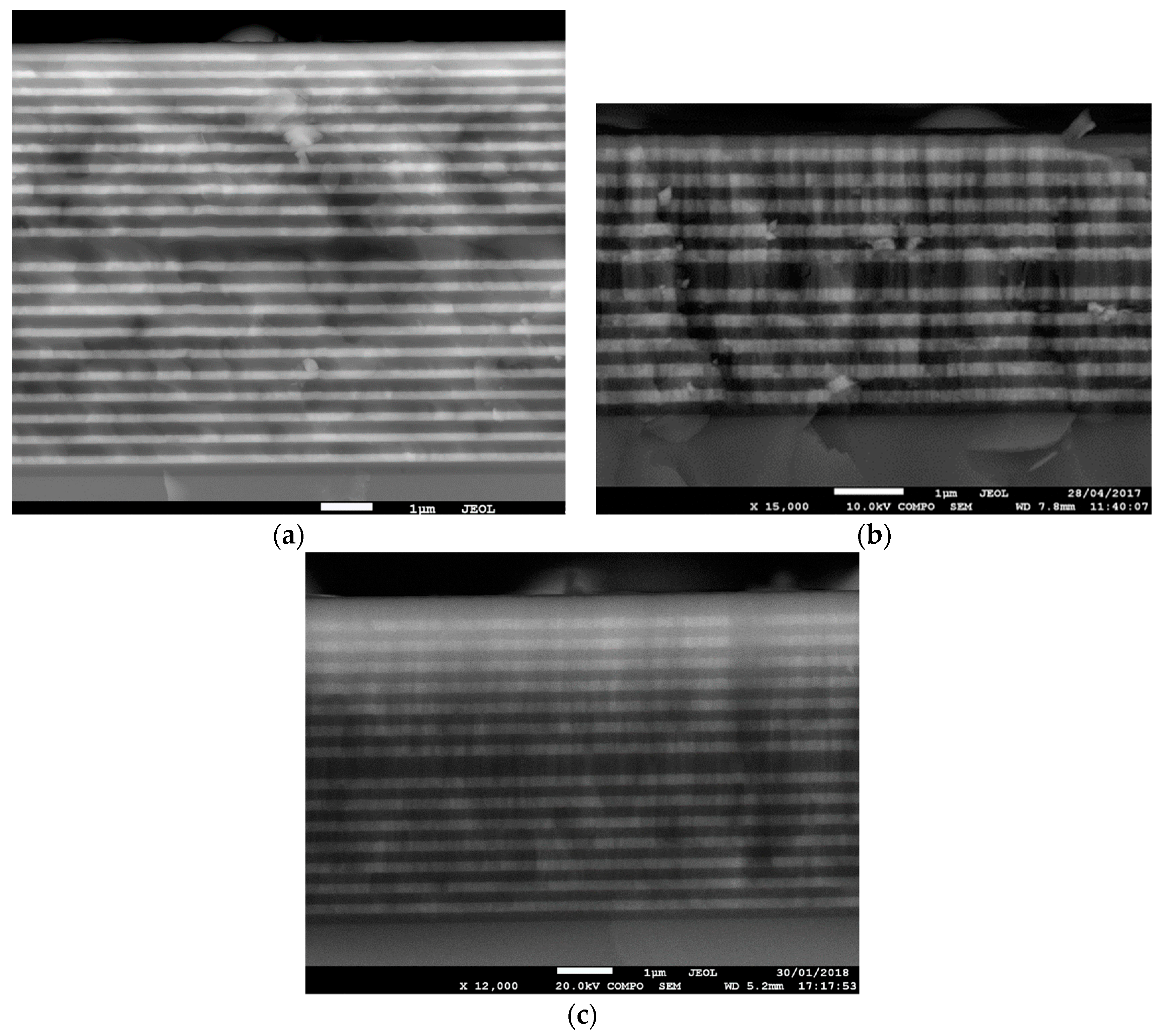
Scanning electron microscope (SEM) micrographs of the all Er
3+ doped 1D dielectric microcavity cross sections are reported in
Figure 1a (PC10), 1b (PC05), and 1c (PC07). The dark regions shown in
Figure 1 correspond to the SiO
2 layer and the bright regions correspond to the TiO
2 layer. The substrate is located at the bottom of the image and the air on the top. It is possible to identify the defect layer and the two Bragg reflectors.
Energy dispersive spectroscopy (EDS) measurements indicated that the erbium content in all the layers was about 0.2 ± 0.1 mol%. The thicknesses and refractive indices of SiO
2 and TiO
2 thin films were measured using an m-line technique in the 1.5 µm range [
16,
27] on reference single SiO
2 and TiO
2 films fabricated using the protocol employed for the photonic crystal. The refractive indices for SiO
2 and TiO
2 were 1.44 and 2.2, respectively. The thickness of each layer was monitored during the deposition using the quartz microbalance. The final thickness of each layer measured using SEM microscopy on the Bragg mirror was 270 ± 5 and 170 ± 5 nm for the silica and titania layers, respectively, and a thickness of 540 ± 5 nm for the SiO
2 doped with Er
3+ defect layer.
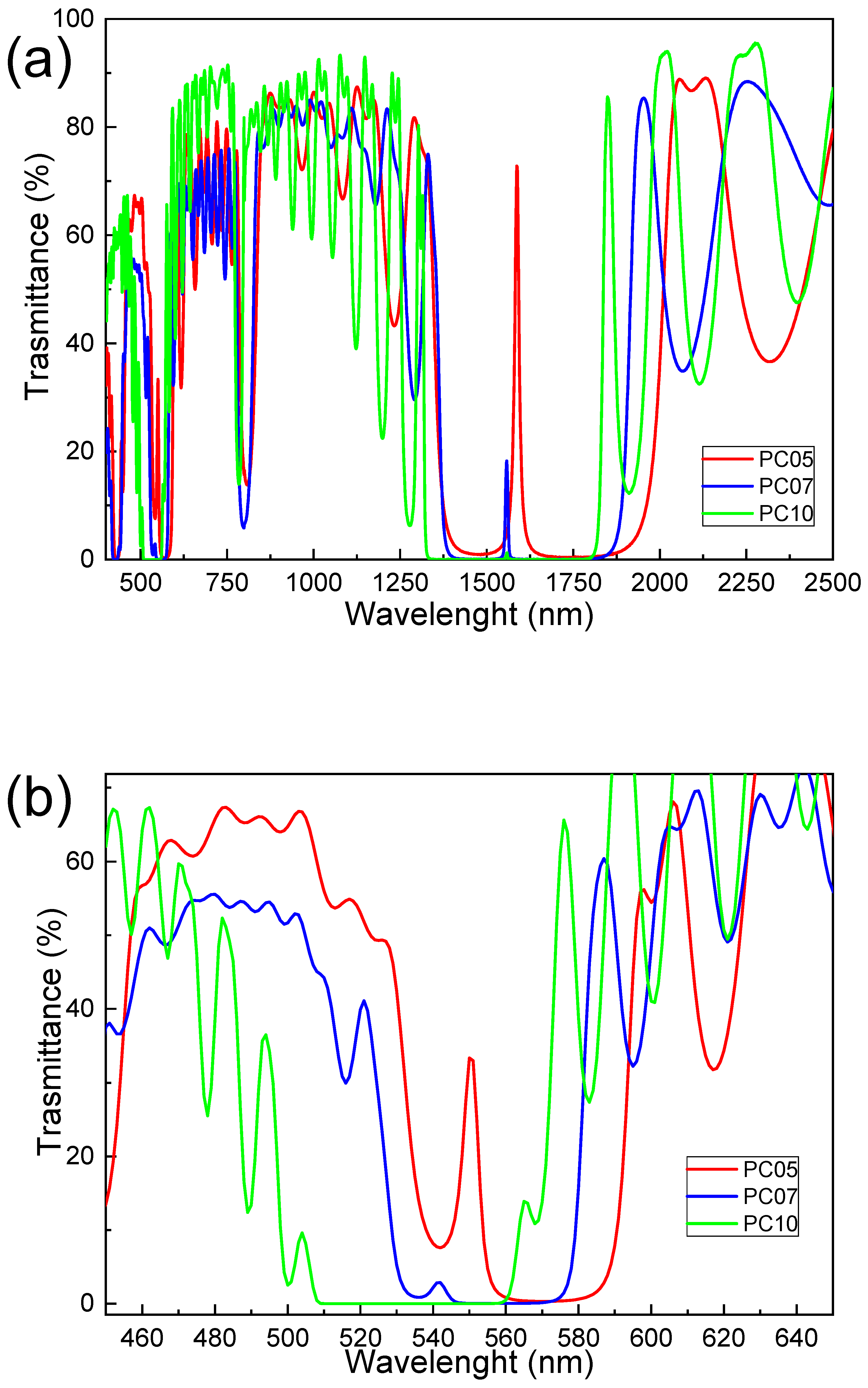
The transmittance spectra of the samples are reported in
Figure 2. It is possible to identify the stop band for the three samples developed, which were from 1400 nm to 1850 nm, as shown in
Figure 2a for the three samples. A sharp peak in the transmission spectra appeared at 1560 nm and corresponds to the cavity resonance related to the Er
3+-doped SiO
2 half-wavelength-thick layer inserted between the two Bragg mirrors. Also, it is possible to observe the third order stop band in the visible region, as seen in
Figure 2b. The third order of the cavity resonance is also present in the stop band, and appears at 530 nm at a 0 degrees incident angle. At a 30 degrees incident angle, the third-order cavity resonance was shifted to 514.5 nm. The quality factor of the cavity was calculated as the ratio between wavelength position of the first order resonance peak and his FWHM. The values are reported in
Table 1.
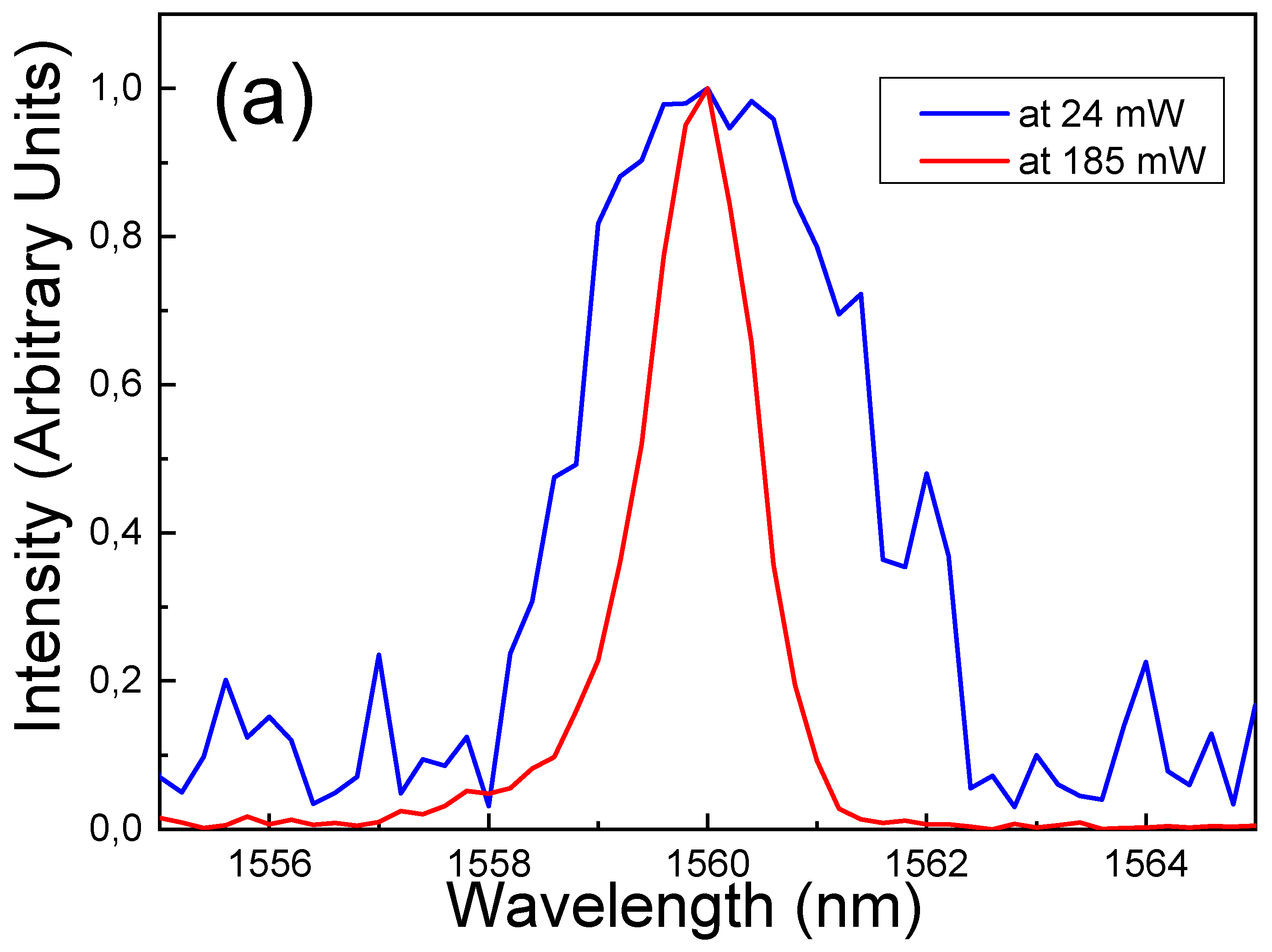
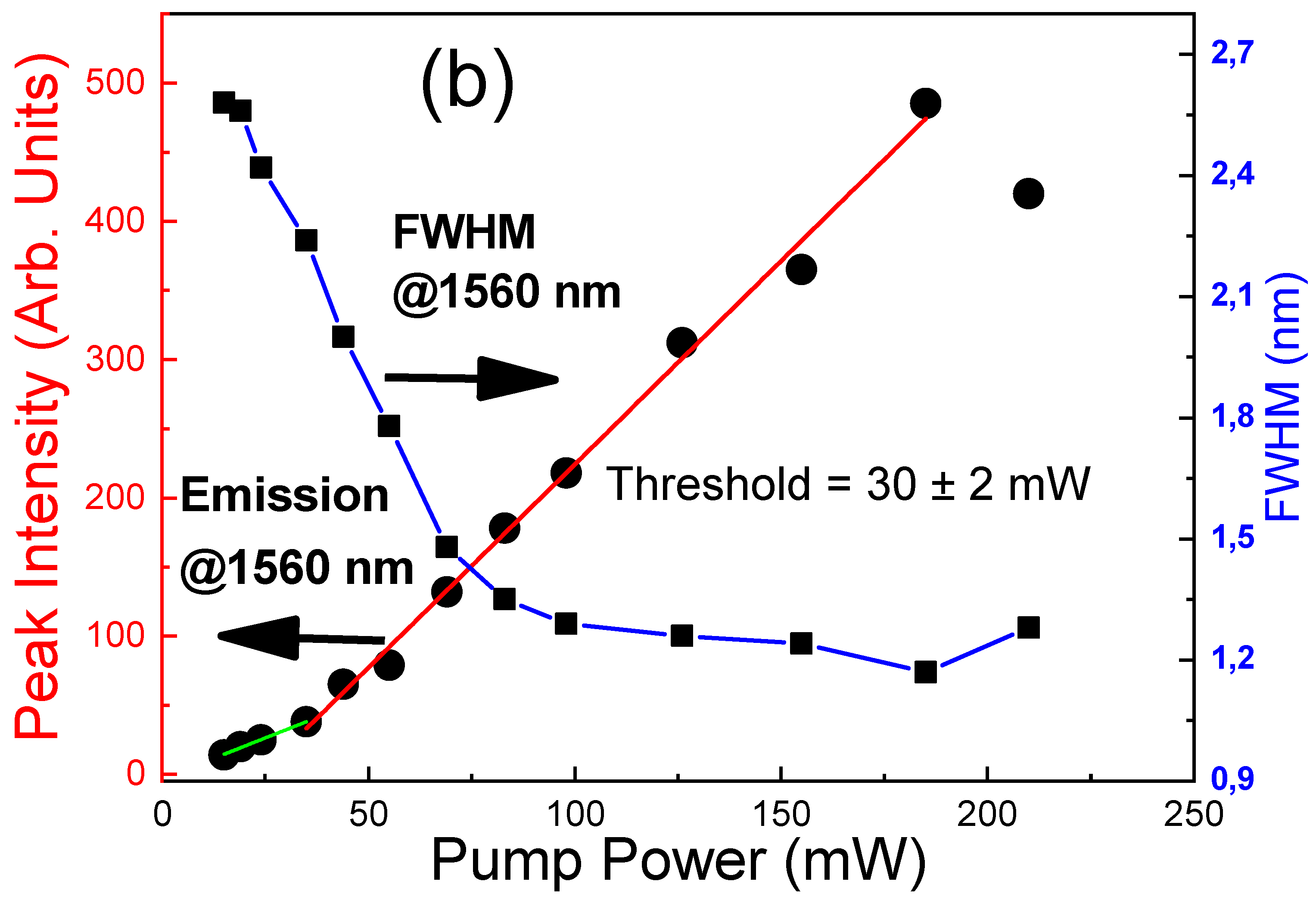
In
Figure 3a, the photoluminescence spectra is reported for the
4I
13/2→
4I
15/2 transition of the Er
3+ ions obtained for the PC10 sample at excitation power at 514.5nm of 185 mW and 24 mW with the Ar+ laser. The erbium emission from the microcavity is centered at 1560 nm with FWHM of ≈1.2 ± 0.1 nm that corresponds to the resolution of the detection apparatus in the case of excitation power of 185 mW, while with the 24-mW excitation, the FWHM was equal to 2.4 ± 0.1 nm. The measurement was performed with a detection angle of 0 degrees and an excitation angle of 30 degrees. In
Figure 3b, the photoluminescence intensity and the FWHM as a function of the pump power is plotted.
In
Figure 4a, the photoluminescence spectra is given for the
4I
13/2→
4I
15/2 transition of the Er
3+ ions obtained for the PC07 sample excited under 514.5 nm with the Ar
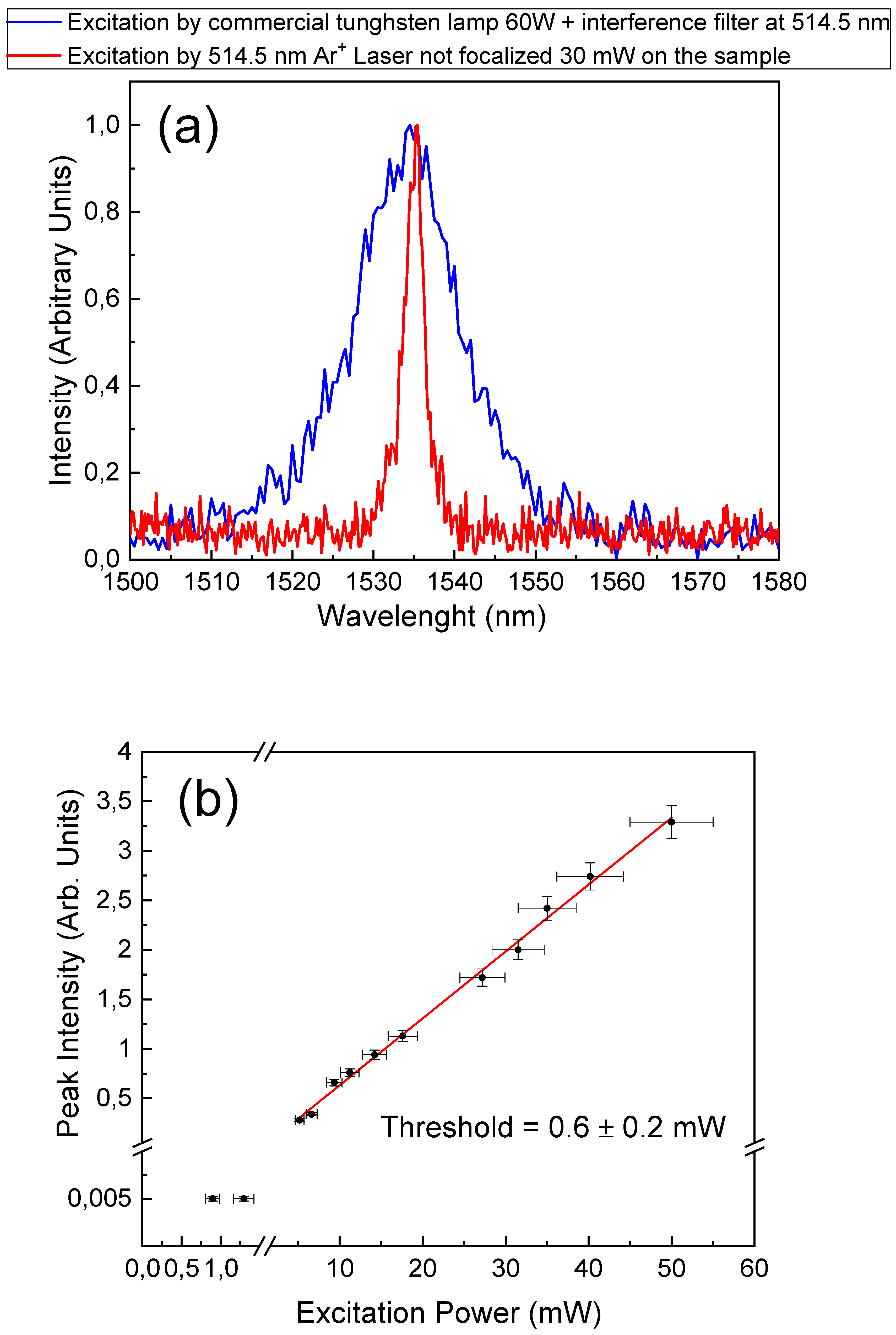
+ laser (30 mW) and with the tungsten lamp filtered by the interference filter (IF). In the case of laser excitation, the erbium emission from the microcavity was centered at 1535 nm with a FWHM of ≈ 2.2 ± 0.1 nm that corresponds to the resolution of the detection apparatus while with the lamp excitation, the FWHM was equal to 14.5 ± 0.1 nm. The measurement was performed with a detection angle of 0 degrees and an excitation angle of 30 degrees. In
Figure 4b, the photoluminescence intensity versus the pump power is given.
In
Figure 5a, the photoluminescence spectrum is given for the
4I
13/2→
4I
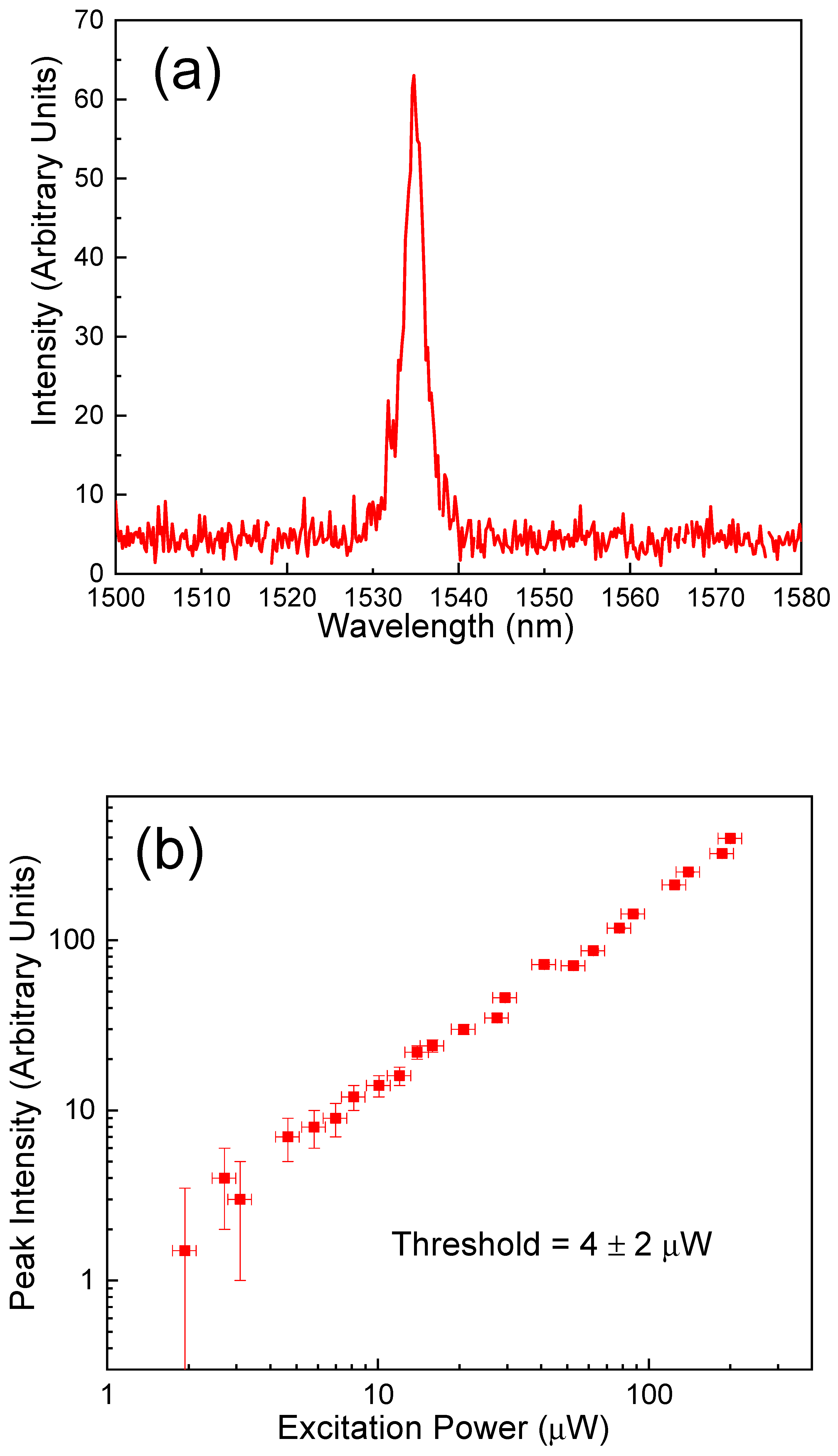
15/2 transition of the Er
3+ ions obtained for the PC07 sample at an excitation power < 1 mW for the Xenon excitation lamp with a monochromator. The erbium emission from the microcavity was centered at 1535 nm with a FWHM of ≈ 2.1 ± 0.1 nm that corresponds to the resolution of the detection apparatus. The measurement was performed with a detection angle of 0 degrees and an excitation angle of 30 degrees. In
Figure 5b, the photoluminescence intensity versus the pump power is given. The linear fit of the experimental data intercepts the x-axis at a pump power value of 4 ± 2 µW.
The transmittance spectra is reported in
Figure 2a and the data summarized in
Table 1 shows that increasing the number of layers in the Bragg reflector increased the quality factor of the structures, but also gave lower transmission values at the resonance peaks. Moreover, the number of defects in the sample increased during the deposition [
22]. These facts suggest that an optimization of the number of layers that composed the Bragg grating was necessary to find the best compromise between the high quality factor and the low threshold. It is important to note that the configuration with seven couples for each Bragg reflector exhibits the lower threshold that passed from 30 ± 2 mW for the PC10 sample to 4 ± 2 W for the PC07 photonic crystal.
4. Discussion
One can note that the top layer of sample PC07, the one in direct contact with air,
Figure 1c, was made of a half-wavelength layer of lower index SiO
2. This extra thickness enabled one to optimize the reflectance of the top Bragg reflector, taking into account the constructive interference between the Bragg reflector itself, and the SiO
2/air Fresnel reflectance at the interface. From the transmittance spectra of the samples, reported in
Figure 2, the stop band for the three developed samples were identified from 1400 nm to 1850 nm, with a sharp peak in the transmission spectra at 1560 nm, corresponding to the cavity resonance. The third order stop band in the visible region was reported in
Figure 2b and it was used for exploiting the cavity resonance, not only for the emission, but also for the pumping of the structure. The sample PC10 experienced a high quality factor, 390 ± 1, and defined PBG, with a minimum transmission of 10
−2. The sample PC05 experienced a lower quality factor, 110 ± 1, with a higher minimum of transmission, around 2%, but an increased transmission at the resonance condition. From the photoluminescence properties of the three samples, reported in
Figure 3a,
Figure 4a, and
Figure 5a, it is clear that all the samples experienced the narrowing of the FWHM when the pump power was increased. This phenomenon can be explained only by considering stimulated emission as the mechanism involved. The observation of coherent emission in such structures is a huge step in comparison to the old works, where only spontaneous emission was provided [
16,
17].
An estimation of the threshold of the samples PC10 and PC05, reported in
Figure 3b and
Figure 4b, respectively, explains the role of the transmission at the resonance condition and of the quality factor in obtaining the decreased threshold. A compromise in obtaining as low a threshold as possible for this system is represented by sample PC07. The transmission characteristics are a compromise between the PC10 and PC05 approach, but the threshold obtained was 4 ± 2µW.
The fabrication of these kind of samples directly on the tip of a fiber is in progress to assess the efficiency of the systems by directly measuring the emitted light in the fiber with an optical spectrum analyzer.

 ,
, 


