Article

Coupled Photonic Crystal Nanocavities as a Tool to Tailor and Control Photon Emission

1
National Research Council, Institute for Photonics and Nanotechnologies (IFN-CNR), Via Cineto Romano 42, I-00156 Rome, Italy
2
Department of Physics and Astronomy, University of Florence, via Sansone 1, I-50019 Sesto Fiorentino, Italy
3
European Laboratory for Non-linear Spectroscopy, via Nello Carrara 1, I-50019 Sesto Fiorentino, Italy
4
Department of Physics, Sapienza University of Rome, P.le A. Moro 5, I-00185 Roma, Italy
5
Dep. Applied Physics and Institute for Photonic Integration, Eindhoven University of Technology, 5600 MB Eindhoven, The Netherlands
*
Authors to whom correspondence should be addressed.
Present address: Instituto de Ciencia de Materiales de Madrid (ICMM), CSIC, Sor Juana Inés de la Cruz 3, 28049 Madrid, Spain.
Present address: Department of Chemistry, University of Cambridge, Lensfield Road, Cambridge CB2 1EW, UK.
§
Present address: National Research Council, Istituto Nazionale di Ottica (INO-CNR), via Nello Carrara 1, I-50019 Sesto Fiorentino, Italy.
Ceramics 2019, 2(1), 34-55; https://doi.org/10.3390/ceramics2010004
Submission received: 29 November 2018 / Revised: 21 December 2018 / Accepted: 27 December 2018 / Published: 14 January 2019

Abstract

:
In this review, we report on the design, fabrication, and characterization of photonic crystal arrays, made of two and three coupled nanocavities. The properties of the cavity modes depend directly on the shape of the nanocavities and on their geometrical arrangement. A non-negligible role is also played by the possible disorder because of the fabrication processes. The experimental results on the spatial distribution of the cavity modes and their physical characteristics, like polarization and parity, are described and compared with the numerical simulations. Moreover, an innovative approach to deterministically couple the single emitters to the cavity modes is described. The possibility to image the mode spatial distribution, in single and coupled nanocavities, combined with the control of the emitter spatial position allows for a deterministic approach for the study of cavity quantum electrodynamics phenomena and for the development of new photonic-based applications.

1. Introduction

The development of fabrication technologies that enable the capability of patterning materials on dimensions smaller than the wavelength of light has opened the way to new classes of applied physics fields, like plasmonics, photonics, spintronics, and also to the experimental exploitation of quantum effects [1,2]. This is of particular interest in the field of optics. The interaction between optical waves (i.e., photons) and materials is strongly dependent on the material structure, so nowadays, it is possible to control and tailor the light propagation and localization by designing the material arrangement. Within this framework, photonic crystals (PCs) represent a perfect example of how, by nanostructuring a material, we are able to impart to it new physical properties. As it is well known, PCs have been introduced starting from the idea of Yablonovitch [3] and John [4], by Joannopoulos and co-workers [5]. The idea is based on the possibility to create a periodic variation in the refractive index of dielectric materials, in order to affect the properties of photons, in a similar way to how ordinary crystals affect the properties of electrons. If the difference in the refractive index of the materials is high enough, and if the absorption of light in the materials is sufficiently low, the refractions and reflections of the light wave through all of the various interfaces can produce the same effects for photons as the ones produced by the atomic periodical potential for electrons (for an extensive description see [5], in particular Chapter 3). As in the semiconductor crystal, the atomic periodic potential gives origin to the band gaps between the valence and conduction energy bands, and in the photonic crystals, the periodic modulation of the refractive index of the dielectric materials allow for the formation of photonic band gaps, that is, a frequency range in which light propagation is forbidden.
Photonic band gaps can be designed and fabricated in dielectric materials with a different refractive index; the propagation of photons can be inhibited for certain designed frequencies and allowed for others. The periodic variation can be realized in 1D, 2D, or 3D, determining the characteristics of the PC band gaps; for example, 3D PCs could have a complete developed band gap and the light cannot propagate in any direction for any wavelength within that gap. A typical 2D PC consists of an array of holes (i.e., air cylinders) realized in a dielectric material slab. The presence of the slab also ensures confinement in the vertical direction by total internal reflection. The symmetry of the lattice, the diameter of the holes (d), the array lattice spacing (a), and the slab thickness (t), are the parameters that control the band gap properties for in-plane propagation. High resolution e-beam lithography and high precision anisotropic etching are the top-down fabrication processes that enable the fabrication of PCs. The control of the fabrication process has a direct influence on the PC performances, and must be carefully evaluated, as we will discuss in the following. Moreover, defects in the PCs can be introduced on purpose, in order to create integrated photonic elements. Linear defects, a missing line of holes, gives rise to waveguides; point defects, namely missing a single hole or a few holes, results in a nanocavity. A single PC nanocavity can be considered as the photonic analogue of a bounded electronic quantum system, and shows a discrete set of energy levels with a characteristic spectral width and spatial extent, even if the photonic is inherently an open system. By combining these basic elements and tuning the characteristic parameters of PCs, integrated photonic circuits and devices can be designed and fabricated to manipulate light at wavelengths ranging from visible to microwaves, according to the resolution limit of the fabrication techniques.
PC nanocavities can be exploited to realize advanced light sources when coupled to two levels emitters, for example quantum dots (QDs). A quantum dot is an inclusion of material, confined in 3D on a nanometric scale into a hosting material with a higher band gap energy, thus resulting in a discrete energy spectrum and in strong carrier correlation effects, making the energy of each electronic configuration (excitons, biexcitons, and multiexcitons) easily distinguishable. According to the density of the QDs grown in the PC nanocavity, several quantum electrodynamic effects can be studied, from the deterministic coupling between a nanocavity and an emitter (Purcell effect [6], Rabi oscillations [7], etc.) to the controlled production of single or entangled photons [8,9,10]. The Purcell effect, or weak coupling, is the modification of the spontaneous rate of emission when the emitter transition is tuned with one of the discrete cavity modes. A faster emission is desirable, because it allows for the realization of more deterministic and reliable single photon sources (photon-on-demand source). Furthermore, the cavity can channel the emitted photons into a well-defined spatial mode in order to increase the extraction efficiency. However, the most striking change of emission properties occurs when the conditions for strong coupling are fulfilled. In this case, there is a change from the irreversible spontaneous emission to a reversible exchange of energy between the emitter and the cavity mode, leading to vacuum Rabi splitting [11]. This coherent coupling may provide a basis for future applications in quantum information processing or schemes for coherent control. To summarize, low-threshold lasers [12,13], single photon sources [8,9], add-drop filters [14], and the implementation of cavity quantum electrodynamics experiments [15,16,17,18] are just some examples of the possible applications of PC nanocavities.
In this review, we describe some of our studies on coupled photonic-crystal cavities, an interesting platform to exploit the features of photonic molecules [19]. Photonic molecules have been employed to realize photonic device like lasers [20], waveguides [21], or memories [22]. The basic photonic structure we considered is a two dimensional triangular lattice with a filling factor of f = 35%, and the analyzed single cavity is formed by four missing holes (see the topography image and scanning electron microscope (SEM) image in Figure 1a,b) [23], and diamond-like and denominated D2. The mode distribution of these D2 coupled PC cavities is particularly interesting and makes them good candidates to study a coupled PC system; a system of two D2 coupled PC cavities has been designed, fabricated, and characterized using photoluminescence (PL), and near field and far field spectroscopy in order to understand the cavity mode behavior. The two-cavity system has been exploited to realize an analogue of the Young’s double slit experiment to probe the photonic mode symmetry and to give an experimental proof of the possibility to control the ground state bonding and antibonding nature in the photonic molecules using the geometrical arrangement. Once the two coupled PC cavities case has been analyzed, we also considered a system of three coupled PC cavities to investigate the photon hopping between the interacting resonators. The control of the mode nature and of the related effects is crucial in the exploitation of photonic molecules as building blocks of large scale photonic integrated circuits in analogy with electric circuits [24].
In order to exploit the coupling effects between the coupled PC cavity modes and the two-level emitters (QD), a spatial and spectral overlap between the PC nanocavity and the emitter is mandatory. Usually, QDs are grown by epitaxial techniques (MBE, MOCVD, etc.). It follows that QDs are randomly positioned and the spatial matching is not easy to implement. Several techniques have been exploited to reach this goal (see, for example, [25,26]). A solution based on nanofabrication techniques and on the unique characteristics of dilute nitride materials, in particular GaAsN, has been proposed and implemented. The characteristic of GaAsN will be briefly described, together with the fabrication process, which allows for the post-growth creation of QDs in controlled positions. This last achievement together with the knowledge of the mode distribution in the coupled PC cavities is crucial in order to realize the spatial and spectral matching between the emitter and the nanocavity, a condition needed to create efficient photonic devices.

2. Material and Methods

With regards the PC coupled systems, the investigated structures have been fabricated on a 320 nm-thick GaAs membrane with three layers of high-density InAs QDs grown using a molecular beam epitaxy embedded at the center of the membrane [27]. If properly excited, the InAs QDs at room temperature are characterized by a bright photoluminescence band centered at 1300 nm and (considering state filling excitation) about 60 nm broad, which acts as an internal light source for the photonic structures. The membrane is grown on a sacrificial layer of AlGaAs on a GaAs substrate. The fabrication process’s initial step is the pattern transfer on a 150-nm-thick SiO2, deposited on the GaAs membrane, by 100 kV electron beam lithography (positive resist ZEP 520A) and the CHF3 reactive ion etching of SiO2. SiO2 acts as a mask for the transfer on the GaAs layer by chlorine-based reactive ion etching. The AlGaAs sacrificial layer is then selectively etched in a diluted HF solution to locally release the GaAs membrane. All of the fabrication process steps ensure the dimension control at the tens of nanometers. As our internal light source is much narrower than the photonic bandgap, we perform the lithographic tuning of the PC bandgap [28] (i.e., we use different values of the lattice parameter a, to spectrally move the PC bandgap around our fixed light source).
To investigate the photonic modes, both near field and far field measurements have been performed. To perform the near field analysis, a commercial scanning near-field optical microscope (SNOM) in illumination/collection geometry, was used. The spatially resolved images were recorded by scanning the probe tip over the sample at a fixed distance (few tens of nm). The sample is excited by a laser diode at 780 nm, coupled into the tip. The emitted PL signal, collected by the tip, is coupled to a spectrometer and is finally detected by a liquid nitrogen cooled InGaAs array. At every tip position, the entire spectrum of the sample is collected with a spectral resolution of 0.1 nm. Figure 1c shows a PL spectrum of a single D2 cavity collected at a fixed tip position. The spectrum is characterized by three peaks, which correspond to the main modes of the cavity (labelled M1, M2, and M3). Figure 1d–f shows the spatial distribution of the PL intensity of the M1, M2, and M3 modes, respectively, and is characterized by a subwavelength spatial resolution of the order λ/5. The spatial resolution is defined as the full width at the half maximum of the profile of the smallest feature that can be resolved by our system.
These maps clearly indicate the main elongation direction of the modes. However, these maps are not detailed enough for resolving the typical features of the local density of states (LDOS) that have been numerically calculated with a finite difference time domain software, and are reported in Figure 1g–i for the M1, M2, and M3 modes, respectively.
To map the LDOS with a better spatial resolution, we implemented the tip-induced spectral shift imaging technique [29]. As the probe is made of dielectric material (silica with a refractive index of about 1.5) and the dimension of its apex is comparable with the dimension of the PC holes, it turns out that the tip itself locally perturbs the dielectric environment of the photonic cavity. In fact, we observe that as the tip approaches the center of the cavity, the modes slightly shift to the red. Moreover, Koenderink and coworker theoretically predicted that the tip induced perturbation is proportional to the local strength of the intensity of the electric field [30]. This prediction has been recently debated in view of the non-Hermitian nature of photonics [31]; still, in the limit of a relative high Q (>1000, to be on the safe side), the previous prediction is quite accurate. Therefore, by reporting on a map the strength of the tip induced spectral shift as a function of the tip position, it is possible to map with a high fidelity the electric field intensity of the cavity modes (see Figure 2).
The spectral shift maps are reported in Figure 1j,l for the M1, M2, and M3 modes, respectively. The comparison of these experimental maps with the calculated LDOS ones, obtained by a commercial three-dimensional finite-difference time-domain (FDTD) code (CrystalWave, photon), showed a clear direct correspondence and a quite striking experimental spatial resolution, better than λ/15. With the same technique, it is also possible to map the broadening of the resonance peaks, which gives important information on the tip-induced losses and on the SNOM detection mechanism [29].
To measure the polarization of the electromagnetic fields associated with the PC optical modes, a SNOM with the polarization control has been exploited [32]. The intensity maps of the PL signal of the optical mode, in the two orthogonal polarization channels, supply an image of the two electric field components in the plane on the PCC.
The PCCs were characterized in far field by a micro-photoluminescence setup using a microscopy objective with a numerical aperture of 0.7. The external cone of view forms with the normal to the sample surface at a 45° angle, and the angular resolution is 8°. For the excitation, we used a solid-state laser emitting at 532 nm. The angularly selected PL emission from the sample was collected with a multimode optical fiber, dispersed by a spectrometer, and detected by a cooled InGaAs array; the spectral resolution is of the order of 0.1 nm.

3. Results

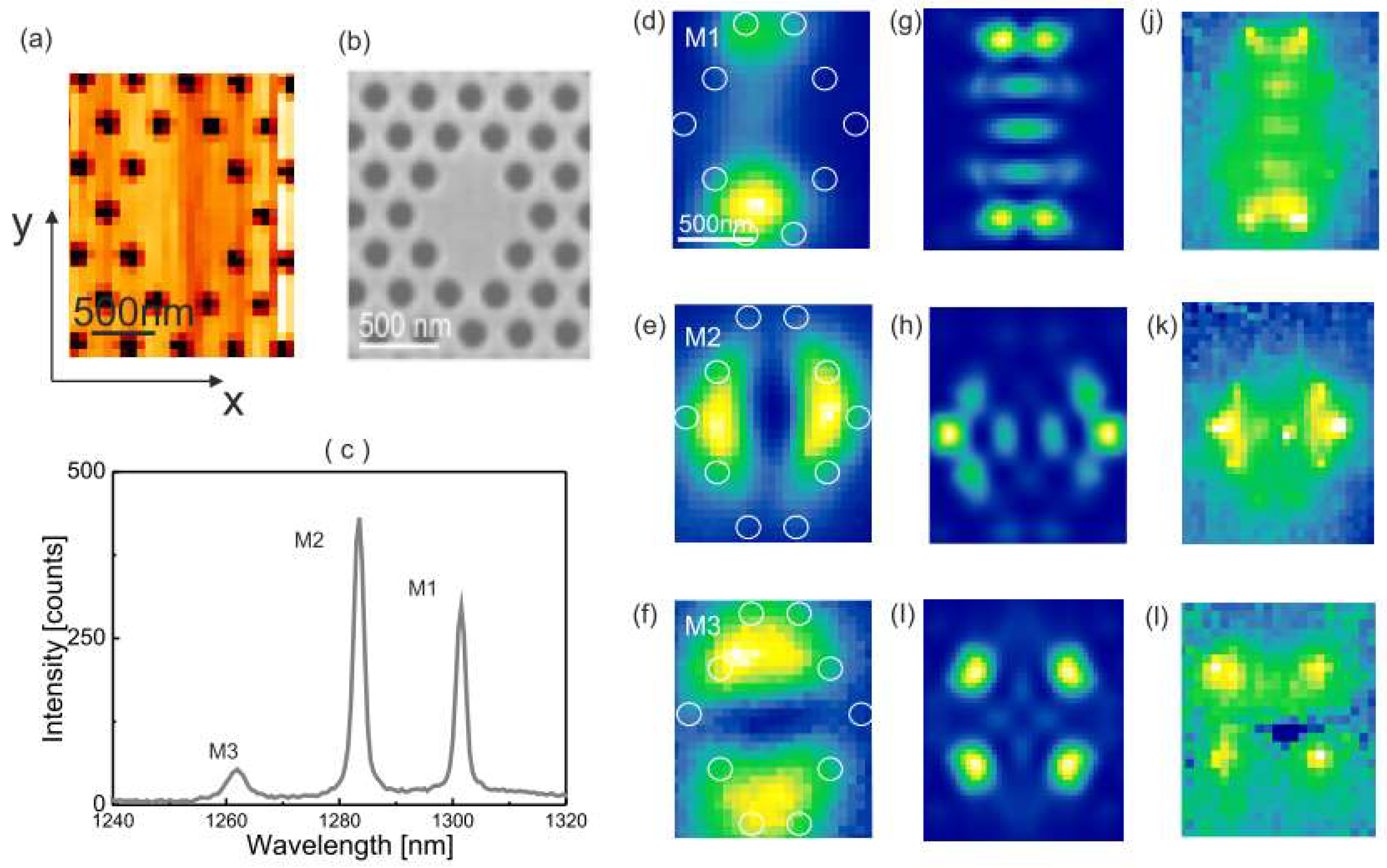
3.1. Photonic Crystal Molecules: Two Nanocavities Case

Two or more interacting PC cavities give raise to the hybridization of the single cavity modes (photonic orbitals), as in real molecules, the inter-atomic coupling gives rise to the molecular orbital. So, the coupled PC cavities can also be called photonic molecules [23,33]. In our case, the coupled photonic nanocavities have been designed in two different configurations; we will refer to vertically (or horizontally) aligned D2 cavities if the coupling line of the two adjacent D2 cavities lies along the principal M (or K) axis of the photonic crystal structure. In the ideal case of identical cavities, frequency matching, and spatial overlap, the coupling results in an energy splitting of the modes and in the formation of delocalized “symmetric” and “antisymmetric” coupled modes. In real samples, we have to take into account the disorder induced by the fabrication process that could determine the presence of a double peak in the spectrum even in the absence of coupling. A given peak can be surely identified as a coupled-cavity mode, only if its intensity distribution is delocalized over the two cavities. On the other hand, if the intensity distribution is localized over one of the two cavities, we observe an uncoupled status. Considering that the coupled cavities system as two linearly coupled oscillators with identical losses (in our case, the modes of each isolated cavity) [23], the formula of the photonic splitting for the coupled-cavity mode can be obtained, Ω = Δ 2 + 4 g 2 , where Δ is the disorder induced energy detuning and g is the coupling energy between the modes of each cavity [34]. Therefore, the photonic splitting Ω is a direct measurement of the coupling energy g only when Δ = 0; in the case Δ ≫ g, the system is uncoupled. So, it is crucial to determine the nature of the coupled PC cavity modes in order to verify the coupling energy and the accuracy of the fabrication process.
To better understand the analysis of the coupled PC cavities, it is necessary to start from the main properties of a single D2 cavity [23]. Figure 1a reports the topographic map of a D2 cavity with a lattice parameter a = 311 nm and a x,y reference system in the plane, with the vertical y axis aligned to the principal diagonal of the D2 cavity. In particular, the M1 mode is elongated along the y direction (Figure 1j), the M2 mode is mainly elongated along the x direction (Figure 1k), while the M3 mode is mainly distributed at the vertexes of a square (Figure 1l). In the analysis of the two coupled PC systems, we will consider only the modes M1 and M2.
Now, we can start with the analysis of the two coupled PC cavities. As seen, the M1 and M2 modes of the D2 cavity have a very distinct LDOS and are expected to show different coupling energy g in the horizontal and vertical coupling design. As we will demonstrate in the following, the nature of the coupled cavity modes is strictly related to the disorder induced by the fabrication process and by the geometry of the system. In Figure 3, the comparison between the experimental results for the horizontally (along x) coupled PC cavities and the calculated electric field intensity is reported. The PL maps indicate that the mode labelled P1 is concentrated on the left cavity (Figure 3b), and the mode labelled P2 is localized on the right cavity (Figure 3c).
The PL signal related to the modes labelled P3 and P4 is instead delocalized on both cavities (Figure 3d,e). The analysis of the spectral shift maps allows for a better understanding of the nature of the different modes, and to correlate them with the modes of a single D2 cavity. The P1 and P2 modes are similar to the M1 mode of a single D2 cavity (Figure 1d), and the coupling energy (g) for the M1 modes of the two horizontally aligned D2 cavities is very small. The spectral splitting of 2.6 meV between P1 and P2 has to be ascribed to the energy detuning due to structural disorder in the cavity realization. In the case of the P3 and P4 modes, the situation is quite different. Their experimental maps strongly suggest that P3 and P4 are the two coupled cavity modes originating from the M2 modes of the two D2 cavities. This is clearly demonstrated by the comparison of the spectral shift map of P3 (Figure 3h), with the corresponding simulated map of the LDOS, as reported in Figure 3j. The spatial distribution of both the experimental and theoretical P3 LDOS is extended over the whole coupled system, and is very similar to the electric field distribution of two M2 modes, (Figure 1h), each centered on one of the two D2 cavities, forming the horizontal coupled system. Analogous results are obtained for P4 (Figure 3e,I,k). Therefore, the large spectral splitting between P3 and P4 is attributed to their electromagnetic coupling, but still, we have to consider that the two D2 cavities are not identical. From the statistical analysis of several single D2 cavities, we found that, even if the absolute position of the M1 and M2 modes shifts up to 9 meV because of a structural disorder, their energy separation varies only up to 1 meV. Therefore, we can assume that the 2.6 meV energy splitting between P1 and P2 is also an estimation of the cavity detuning for the two M2 modes. Therefore, by using Ω = Δ 2 + 4 g 2 , we obtained a coupling parameter of g = 5.9 meV for the M2 modes in the horizontal (along x) geometry.
In the case of the vertically (along y) coupled PC cavities, we found a different situation. In Figure 4, the experimental results are shown. The modes labelled P1 and P2 are delocalized over the entire system (Figure 4b,c; PL maps), and can be attributed to the two coupled-cavity modes originating from the M1 mode of a single D2 cavity (Figure 4f,g; spectral shift maps) with an overall photonic splitting of Ω = 11.7 meV. This attribution is also validated by the simulated map of the LDOS for P1 (Figure 4j). Similar results are obtained for P2. The modes labelled P3 and P4 show a very small splitting (0.8 meV), which cannot be attributed to a structural disorder. As seen before, the signature of the frequency induced mismatch because of the structural disorder is the localization of the modes on the single D2 cavities. Looking to the near field maps of the modes (Figure 4d,e,h,i), it is clear that they are extended over the entire system and can be considered as the symmetric and anti-symmetric coupled cavity modes coming from the M2 mode of the two D2 single cavities. This demonstrates that in this case, the disorder induced by the fabrication process is smaller than the coupling energy, and the matching condition are satisfied. The measured detuning is Δ = 0.8 meV and the calculated coupling energy is g = 5.9 meV for the M1 modes and g = 0.4 meV for the M2 modes. These results are confirmed by numerical simulations.

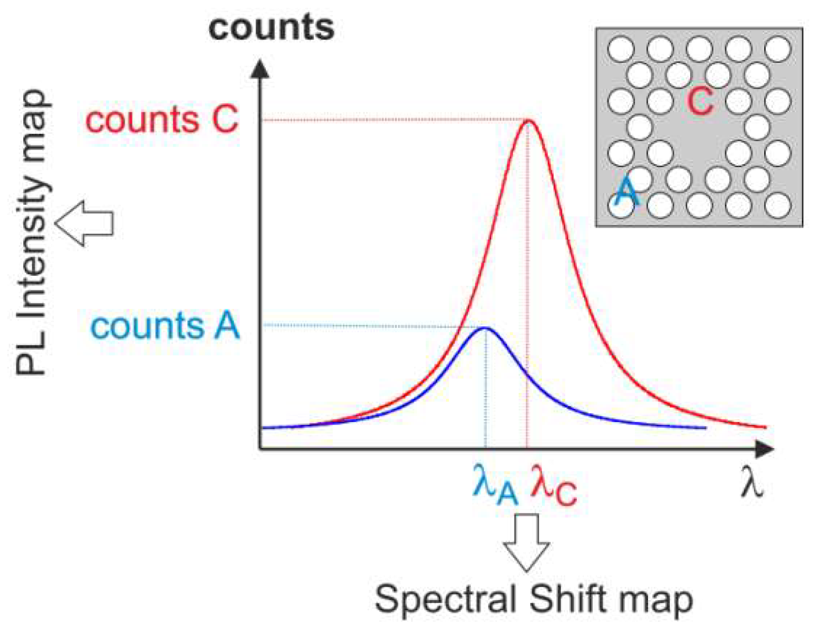
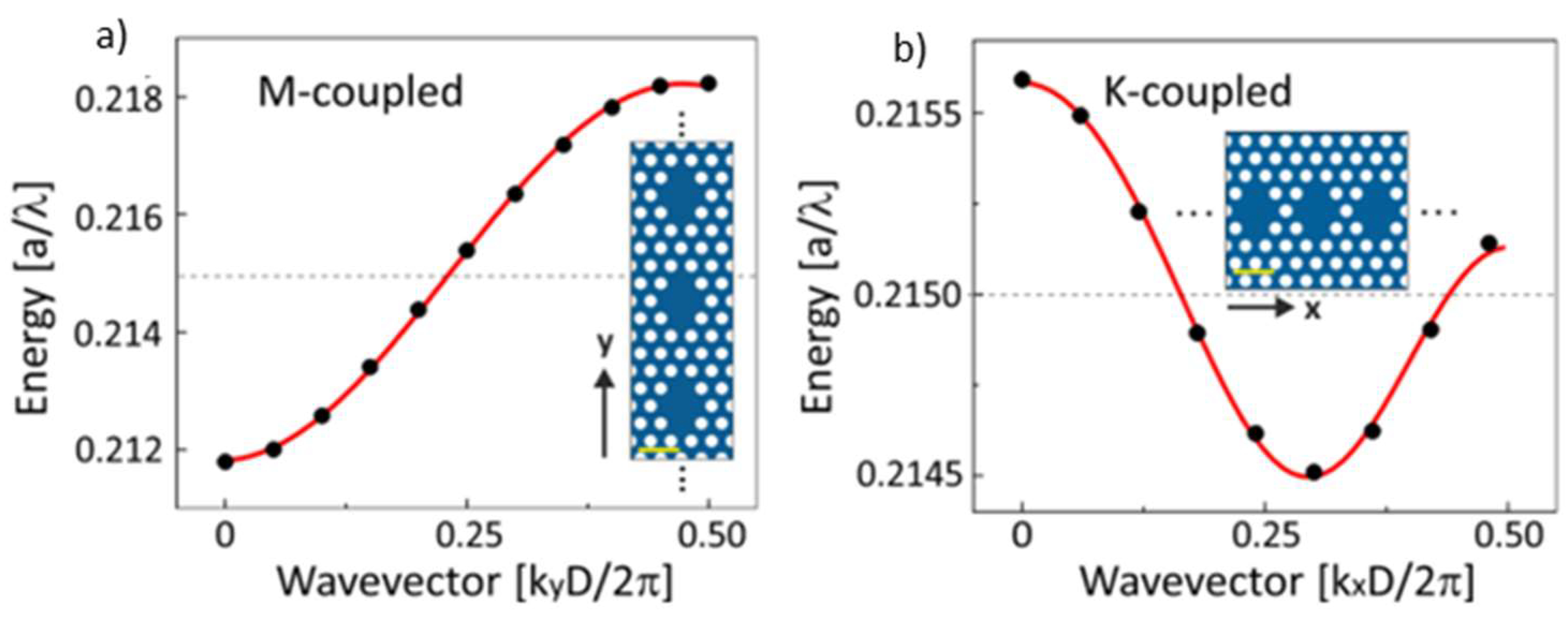
3.1.1. Mode Symmetry

After the comprehension of the mode distribution and the demonstration that the transition from the localized to non-localized mode is controlled by the mode detuning, the symmetry of the coupled modes have been verified in details [35]. This property depends on the phase characteristics and it is not trivial to be measured in the near field; we demonstrated that it is possible to probe it using a far field photoluminescence analysis by considering the two coupled PC cavities in analogy with Young’s double slit experiment. Several phase sensitive techniques have been proposed in near field and far field [36,37], but the method we proposed is quite simple and straightforward.
In an ideal photonic molecule, the mode coupling determines the frequency splitting of the eigenvalues, originating in the delocalized symmetric and antisymmetric eigenvectors. The symmetric mode, E + [ r ] , arises from two in-phase single cavity modes and a constructive interference along the normal direction, and is expected to be observed (as in the original Young’s double slits experiment). The asymmetric mode, E [ r ] , arises from two out of phase single cavity modes, and a destructive interference along the normal direction is expected. The coupled modes can be described as a linear superimposition of the single cavity modes, depending on the spatial distance between the cavities. The symmetry of the single cavity modes has a very strong impact on their angular emission pattern, as can be deduced by analyzing the Fourier transform of the coupled modes. Starting from these considerations, the far field patterns of the coupled modes have been calculated on the basis of the numerically simulated far field patterns of the modes of the single cavity. As before, we refer to the single cavity modes as M1 and M2, and to the coupled cavity modes as P1–P4. So, to exploit the effects of the Young’s double slit interference to probe the mode symmetry of a photonic molecule, we need to measure the polarization resolved far field patterns of the single cavity modes and to estimate the corresponding near field patterns using FDTD calculations (Figure 5), which are linked by a Fourier transform.
The mode M1 is mainly polarized along the x direction, while the mode M2 is characterized by an elliptical polarization [32]. The calculated near field maps show the electric field amplitude with a scale color to indicate the amplitude sign. The measured far field intensity k patterns are shown on a blue background for the PL experimental data and on a black background for the FDTD simulations. We used the denomination x-even (x-odd) for an even (odd) mode with respect to the x inversion, and similarly for y, to describe the mode parity synthetically. With regards the FDTD near field maps, the mode M1, elongated along the y direction, is an x-even and y-even mode (Figure 5c). The mode M2 is more symmetrically distributed (with a slight elongation along x) and the two polarizations have an opposite parity. The x polarization is x-even and y-odd, while the y polarization is x-odd and y-even (Figure 5d,e). The corresponding PL far field intensity k patterns are very different for the following three cases: M1 shows a horizontal stripe with a maximum at the center (Figure 5i). M2 shows a dark central region that is vertical for the x polarization and horizontal for y polarization (Figure 5j,k). The experimental data show a very good agreement with the FDTD simulations (Figure 5f–h). The far field k patterns directly follow from the near field maps, and the following two points help for understanding them: (i) Diffraction imposes that the far field pattern is elongated in the perpendicular direction with respect to the near field map (see M1). (ii) The x-odd (y-odd) modes destructively interfere in the far field along kx = 0 (ky = 0) (see the two polarizations of M2).
With all of these considerations in mind, we can analyze the results for coupled PC structures. In the case of the vertically aligned photonic molecule, we limit our analysis to the P1 and P2 modes arising from the overlap of the two M1 modes (see Figure 6). Following an analysis similar to the single cavity modes, comparing the PL spectra, the experimental PL k patterns of P1 and P2, and the Young’s predictions (with red frames) for constructive and destructive interference, respectively (see Figure 6), we could demonstrate that P1 is the symmetric coupled mode and P2 is the antisymmetric coupled mode. The FDTD simulations (shown in Figure 6f,g) agree well with the data and with the Young’s model predictions.
In the case of the horizontally aligned D2 photonic molecule, the situation is more complex. We analyzed the P3 and P4 modes arising from the overlap of the two M2 modes of the single cavity, which shows elliptical polarization. So, in this case, we have to separately analyze the far field patterns for the x and y polarizations of P3 and P4. As for the vertically aligned case, the results are summarized in Figure 7. From the comparison of the numerical predictions and the experimental measurements, it is possible to affirm that, with regards to the x polarization, P3 and P4 are the antisymmetric and symmetric coupled modes, respectively. In the case of y polarization, the understanding of the far field k patterns of P3 and P4 is not straightforward. The fingerprint of the destructive interference for P3 is the broadening of the dark region along the kx = 0 direction. Instead, the fingerprint of the constructive interference for P4 can be identified in the two additional vertical dark fringes around 40°. A detailed explanation can be found in the literature [35], together with the analysis of the FDTD near field maps of the electric field amplitudes, and it is really worth discussing these last ones, because from them, we can retrieve the parity of the modes that does not always coincide with the symmetry/asymmetry of the modes. For vertical coupling, P1 is y-even and P2 is y-odd, as expected. Instead, for the horizontal coupling, the situation is again more complicated. In this case, it is the x-symmetry that defines the Young interference. The P3 mode is x-odd for the x polarization and x-even for the y polarization. Instead, the two polarizations of the P4 mode have an opposite x-parity with respect to P3. These puzzling parity properties of P3 and P4 can be understood by simply noting that the “symmetric” mode, E + [ r ] , is x-even (x-odd) whenever the electric field mode of the single cavity is x-even (x-odd). On the contrary, the ‘‘antisymmetric’’ mode E [ r ] is x-odd (x-even) whenever the electric field mode of the single cavity is x-even (x-odd). This means that the parity (with respect to inversion) and symmetry with respect to the mode building do not always coincide, and that the orientation of the coupled PC cavities determines the mode properties.

3.1.2. Controlling Bonding and Antibonding Ground State

After the demonstration of the possibility to control the symmetry and parity of the coupled PC cavities modes by the geometrical arrangement, a further step forward was done. Theoretical studies on two coupled PC cavities showed that the ground state in the photonic crystals may actually change from a bonding to antibonding character depending on the spatial alignment or the distance of the two isolated cavities [38,39]. In this case, the analogy with the quantum mechanics is not observed; when a degenerate electron ground energy level of two identical atoms splits into two states through electronic couplings, the lower (higher) energy state always has an even (odd) parity independent of the atomic distance. By using the same Young’s type experiment, it has been possible to demonstrate the different behavior of the photonic molecules and the capability of tailoring the mode nature by the coupled PC cavity design [40]. Again, we investigated the system of two D2 PC cavities, coupled in a vertical (principal axis of the photonic crystal, M) and horizontal (K axis) configuration. By means of the FDTD solver package, numerical simulation of the x component of the electric field of ground (G) and the first excited (E) states of the M and K photonic molecules have been carried out. Both G and E derive from the coupling of the ground modes of the two D2 coupled PC cavities, which are even along both the M and K axes. For the M coupling (vertical), a large mode overlap is found (energy splitting Ω =12 meV) and the mode parity must be considered with respect to the spatial inversion to K axis (horizontal) and the predicted G mode parity is even (E is odd), in accordance with the quantum mechanics analogy. Instead, in the case of K coupling, the observed overlap is small (Ω = 0.4 meV) and the parity is considered for the spatial inversion with respect to the M axis. In this case, the predicted G mode is odd (E is even). So, in this case, the G mode should have an antibonding nature. To experimentally prove these numerical previsions, we had to keep in mind the analysis of the energy splitting Ω for the two coupled PC cavities. When the Ω value is small, we have to verify that this is not because of the possible disorder induced by the fabrication process. Therefore, in the M alignment, because of the large value of the coupling energy, we can neglect the disorder component; in the K coupling, instead, we have to be sure to eliminate the possible detuning coming from the disorder. To do this, many techniques are available, like the local change of the refractive index by liquid infiltration [41] or nano-oxidation [42].
Here, we choose to tune the mode cavity by laser assisted local oxidation [43,44]; the laser exposure allows for photoinduced oxidation and produces a blue shift on the cavity photonic modes. The spatially resolved PL has been used to detect and monitor the spatial localization of the photonic modes of the cavity. The red-shifted mode of the K coupled system has been exposed at steps of about half an hour, at a power of 1 mW. An anticrossing curve has been obtained and the initial experimental splitting of Ω = 1.6 meV could be reduced to a minimum value of 0.9 meV after a total exposure of 150 min. In Figure 8, the comparison between the FDTD calculation and the experimental data for the G (a) and E (b) state in both the M and K configuration are reported. As we know, the far field intensity patterns give direct insight on the mode parity. Even the modes originating from the in-phase single cavity modes and the odd modes come from the out of phase single cavity modes. Following the Young’s analogy, in the first case, we expect constructive interference, and in the second one, a destructive one, along the axis perpendicular to the alignment direction. The far field pattern of the G mode of a single D2 cavity is a bright horizontal band (see Figure 5i). So, the bright horizontal line present in the far field pattern of the M (vertical) coupled PC cavities in Figure 8a, is evidence of the evenness of the G mode, and the dark vertical line in far field patterns of the K mode indicates that its G mode is odd. The numerical results confirm the experimental outcomes. These results mean that the G state is bonding for the M coupling and antibonding for the K coupling, demonstrating that in photonic molecules, the G state can have both a bonding and antibonding nature, and that this property can be controlled by the cavity geometrical design. With regards to the E states, the results are shown in Figure 8b. Also, in this case, the agreement between the numerical previsions and experimental results is very good. The presence of a dark horizontal band in the middle of the far field pattern of the M coupling mode for the excited case, is the fingerprint of the oddness of E mode and of its antibonding nature. Instead, the far field pattern of the E mode in the K coupling shows a bright central spot deriving from the product of the horizontal band of the single D2 cavity by the vertical constructive bright fringe because of the evenness of the E mode in K coupling.
The physical origin of this behavior can be ascribed to the role played by the optical evanescent waves. In an atom, the amplitude of the electron wave-function decays exponentially with the distance from the nucleus. In the photonic crystal case, instead, the localization of the photons is due to the strong multiple scattering, and the field of localized photons oscillates with an exponentially decaying envelope. In the case of the coupled PC cavities, the interference between the oscillatory evanescent electromagnetic waves determines the number of nodes in the total waves and depends on the distance between the sources [45]. Therefore, it is this oscillating nature of the evanescent waves in the photonic band gap that originates the bonding or antibonding nature of the G state of the coupled PC system.

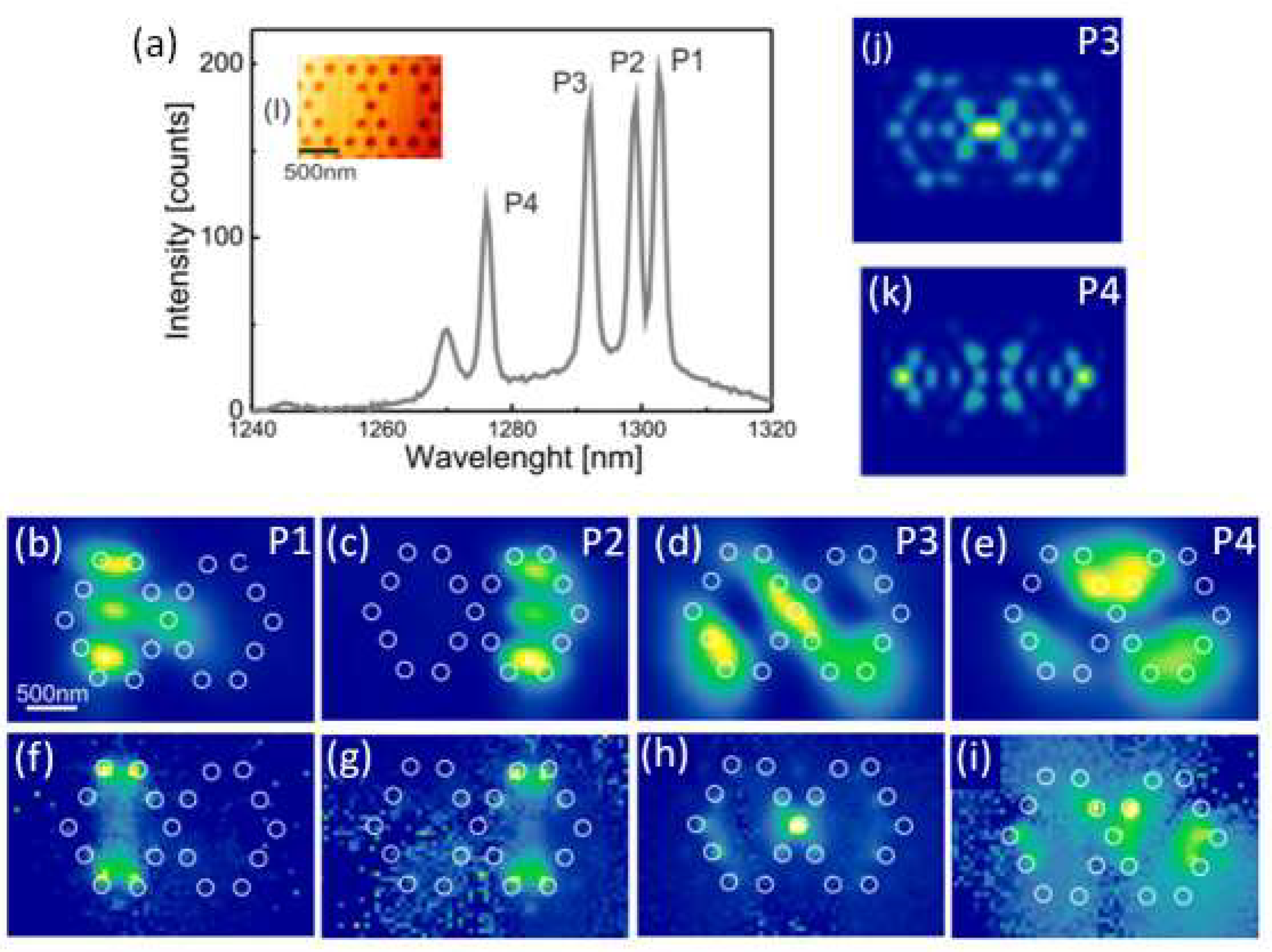
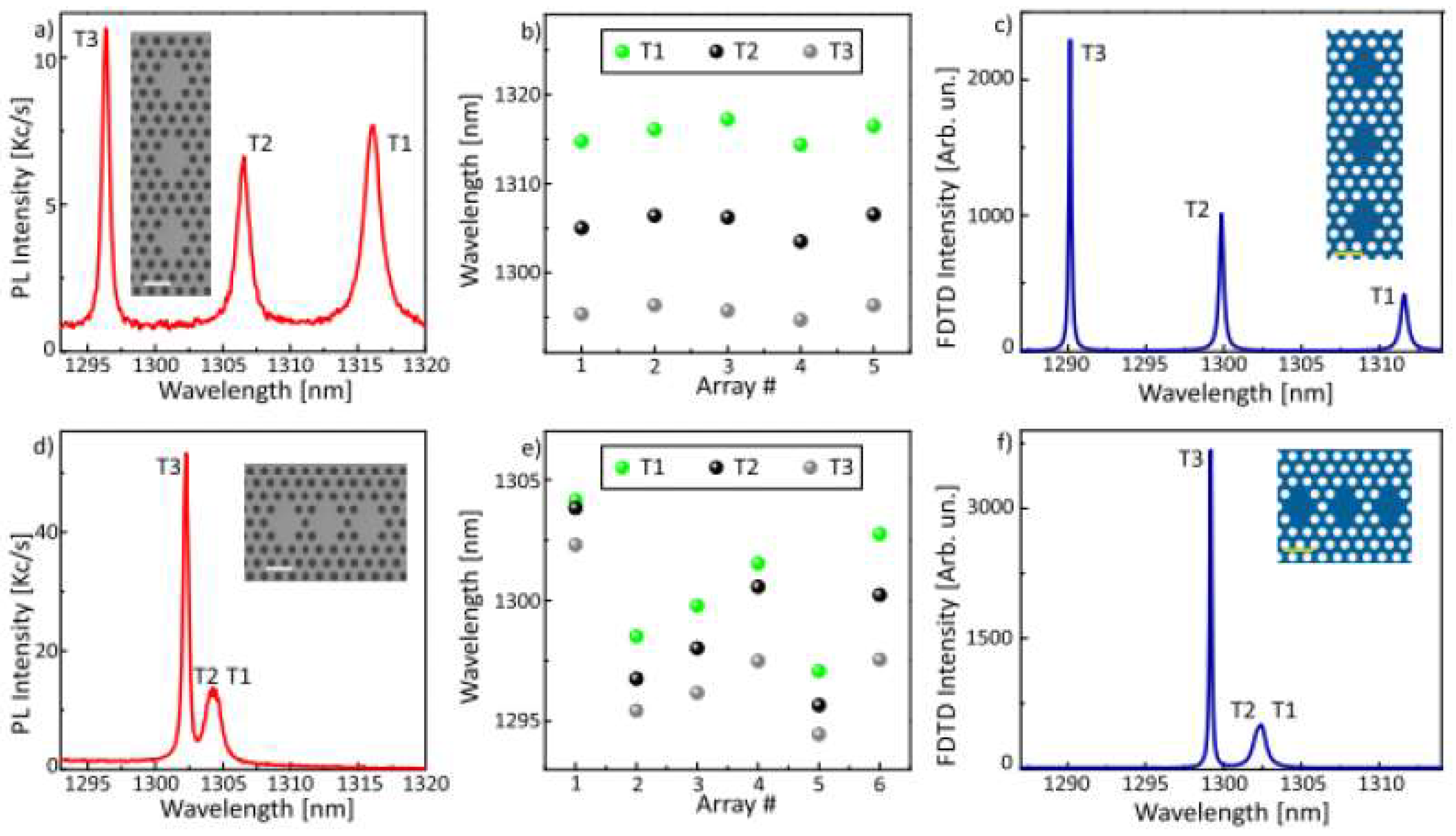
3.2. Photonic Crystal Molecules: Three Nanocavities Case

To continue the study on the photonic molecules, we also designed, fabricated, and characterized the photonic systems made of three D2 coupled cavities along the two principal axes (x and y) [46]. The systems of identical coupled PC cavities, also named photonic arrays, are characterized by spatially delocalized optical modes and spectral minibands, which allow for photon hopping between the adjacent resonator (in analogy with coupled resonators) [47,48]. In this section, we will briefly describe their main properties. In this case, either the nearest neighbor, and the next nearest coupling must be taken into account. As in the two cavity molecules, the geometry plays a crucial role; the mode splitting and spatial distribution depend strongly on the cavity arrangement. To study the behavior of the three-cavity photonic molecule, we considered the coupling between the lower energy mode of each single D2 cavity. As we know, this mode, named M1, is elongated along the M axis (y direction) of the photonic crystal. The consequence of this characteristic is that in the M coupled cavities, the mode overlap is large, similar to what we have described for the two coupled PC system, and so it is the nearest-neighbor interaction. Instead, in the case of the K alignment, the mode overlap is smaller, determining a non-intuitive mode behavior. The theoretical studies of this system have been widely described in the literature [46]. Here, we report on two-dimensional plane wave expansion calculations used to reconstruct the system dispersion curve, and more extensively on the experimental outcomes, whose results validated the theoretical predictions.
Figure 9 shows the mode dispersion relation of a two-dimensional infinite array of the D2 coupled PC cavities plotted in the energy range relative to the fundamental mode of a single D2, for both kinds of M and K alignment. The finite width of both of the dispersion curves demonstrates the real photonic hopping between the coupled PC cavities. Clear minibands appear for both configurations, but with different behavior. In the M alignment, the energy of the photonic guided mode increases monotonically as a function of k, corresponding to a mode with a positive group velocity; in the K alignment, the dispersion of the photonic mode is small and non-monotonic. The group velocity changes its sign at kxD/2π = 0.25, and the light propagation behavior is not trivial. In this case, the interaction between next-nearest-neighbors or distant cavities must also be taken into account. To calculate the neighbor coupling terms, the tight binding approximation has been applied. In Figure 10, the near field PL spectra averaged on the whole array structure are reported for both the M- and K-alignment. Three peaks are detected (denominated T1, T2, and T3) for decreasing the wavelength. In Figure 10b, the peak positions of T1, T2, and T3 for the M aligned cavities with a nominal identical design are shown. The peaks are almost equally spaced at 10 nm. It is important to note that we observed a few nanometers spread in the peak positions, but the separation between T1–T2 and T2–T3 is almost the same, and so the spread is between the T1–T3 modes (about 20 nm). This means that the detuning due to the fabrication process and the possible variation of the membrane thickness is small enough to not impact on the mode coupling in the case of M aligned cavities. For the K alignment geometry, the result is shown in Figure 10d and the peak positions are summarized in Figure 10e the for nominally identical structures. The three mode peaks for each structure are within a 5 nm range, smaller than the M case, denoting a weaker coupling. The peak position spread instead is much higher, so in this case, the fabrication disorder is significant and comparable to the mode coupling. The array #1 is the one in which the disorder is less important; its PL spectrum is reported in Figure 10d, where an almost degeneration in the mode T1 and T2 is observed. In our sample, the array #1 represents the fabricated structure nearest to the theoretical system of the three identical coupled PC cavities, as it is possible to verify by comparing the experimental PL spectrum with the FDTD calculated one (Figure 10f). We also mapped the PL intensity at the peak wavelength for each resonant mode as a function of the SNOM tip position, in order to study the electromagnetic field distribution of the modes, and, to understand the mode behavior, a minimal model based on a three coupled resonator has been developed. In the M aligned structures, the T1 and T3 modes are mainly localized on the central cavity. The T2 mode instead is localized on the external coupled PC cavities. These results confirmed the FDTD simulations and the fact that all of the modes are roughly formed by a linear combination of the single cavity modes. So, the M alignment case can be reproduced considering only the nearest-neighbor coupling.
In the K aligned structures, we observed a complex behavior. The T3 mode is mainly delocalized on the two external coupled PC cavities. The T1 and T2 modes are mainly distributed over both the central and left side coupled PC cavities. The comparison of the FDTD calculations shows that a better agreement would be obtained by exchanging the T1 and T2 distribution. This could happen because of the detuning due to the fabrication disorder and because the two modes are almost degenerate. In the K-alignment model, the contribution of the next-nearest-neighbor has been included together with the nearest neighbor. In this case, the comparison between the experimental and modelling shows some discrepancy, and the real system is proven to be more complex than a three coupled resonator system. Part of the complexity is surely due to the disorder induced energy detuning; nevertheless, this last one can be compensated and tuned by post fabrication techniques as we have seen in Section 3.1.2. The dielectric environment of the coupled PC cavities can be finely modified and in this way resonances between the coupled PC cavities, and so the photon hopping between the adjacent resonator can be controlled on demand. The case where the photon hopping rate is the same for all of the resonators represents the starting point for studying quantum many-body phenomena with light [49,50]. The possibility of controlling the resonance between the adjacent resonators using post fabrication tuning methods and introducing a uniform and controlled gradient in the photon hopping rate between the different cavities allows for engineering photonic arrays suitable for quantum information processing and optical communication.

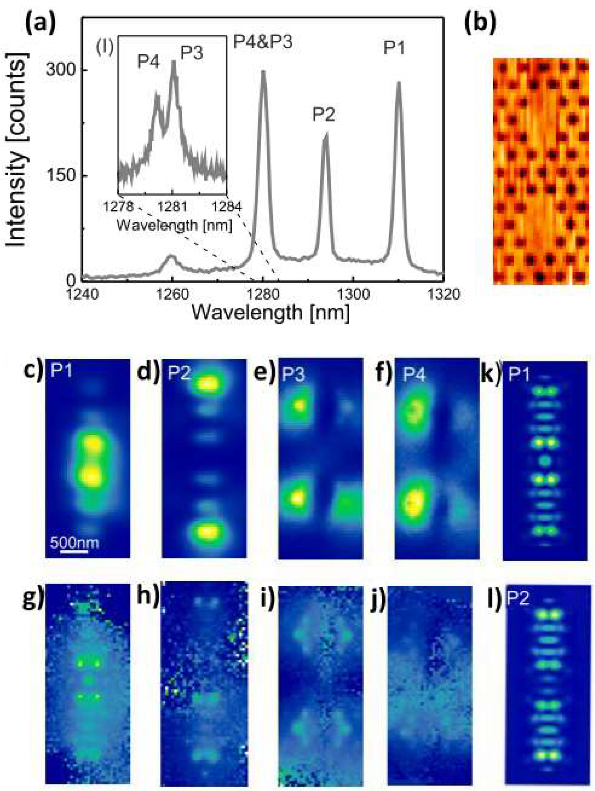
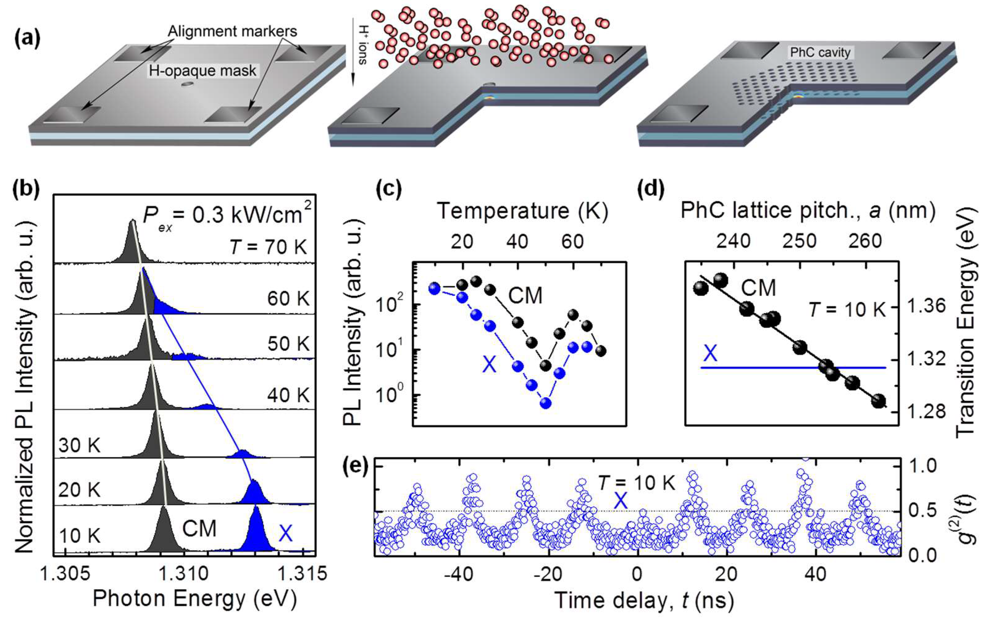
3.3. All Lithographic Approach to PCC and QD Coupled Systems

As detailed in the previous sections, the ability to fabricate photonic crystal structures with a high spatial resolution might open the way to the realization of novel optical elements, which are useful for the manipulation and routing of light in nanophotonic circuits operating at the sub-wavelength level. Equally important, within this context, would be the possibility to integrate one or more light emitters at prescribed points of such photonic circuits. Ideally, the spatial and spectral position of these emitters should be controllable with a precision of a few nm; moreover, they should be able to generate non-classical light states “on demand”, that is, exactly one photon [17] or one entangled photon pair [18] should be produced for each excitation pulse. In recent years, semiconductor quantum dots (QDs) have emerged as particularly promising candidates for the realization of non-classical light emitters [16,51], owing to their inherent integrability with optoelectronic devices, as well as to continuous improvements in terms of their single-photon purity/indistinguishability and degree of entanglement [22,52]. The ability to control the position and emission energy of QDs has also made great strides in the past decade, because of the joint efforts of several research teams [26,53].
Recently, a novel and versatile approach for the post-growth fabrication of site-controlled QDs has been developed based on the spatially selective incorporation or removal of hydrogen atoms in dilute nitride structures [54,55]. Hydrogen incorporation in GaAsN results, indeed, in the formation of N–H complexes, which neutralize all of the effects of N on GaAs, including the N-induced large reduction of the bandgap energy [56,57]. Therefore, by engineering the spatial incorporation and/or removal of hydrogen in dilute nitrides, it is possible to attain a spatially controlled modulation of the bandgap energy in the growth plane and, eventually, to tailor the carrier-confining potential down to a nm scale, resulting in the fabrication of site-controlled QDs that are able to emit single photons on demand [54,55]. Such a novel fabrication approach has made it possible to obtain a fully lithographic approach for the deterministic integration of a site-controlled QD in a PC system [58]. The fabrication process is sketched in Figure 11a. The sample is first provided with a series of Cr/Au alignment markers by means of a standard lift-off process. Then, an ordered array of GaAsN QDs is realized aligned with the metallic markers, by making use of the spatially selective hydrogenation approach described in the literature [54,58]. After the fabrication of the QDs, a photonic crystal cavity can be realized around each QD. The PC cavity fabrication follows a standard procedure that consists of covering the sample with a thin layer of positive-tone electron-beam resist (ZEP520A), on which the desired PC pattern is realized by electron beam lithography (EBL). The resist acts as a mask during the transfer of the PC design onto the sample via the Cl-based dry etching of the GaAsN/GaAs layer. Finally, the mask resist is removed by a wet etching in hot anisole, and the membrane containing the PC structure integrating the GaAsN QD is released by the wet etching of the AlGaAs sacrificial layer with a 5% solution of hydrofluoric acid, in order to provide vertical optical isolation. It is worth mentioning that the presence of the alignment markers on the sample—together with the spatial accuracy in defining the QD and PC cavity both given by the EBL—guarantees a spatial coupling between the QD and the cavity of about 20 nm (limited only by the realignment precision of the EBL system). Further details on the fabrication process can be found in the literature [58]. As summarized in Figure 11b–e, integrated QD-PC systems have already been successfully realized using the fully lithographic approach, and their properties have been optically characterized [57,58]. The energy of the fundamental cavity mode of a series of L3 photonic defects (wherein the microcavity is obtained by removing three holes from an otherwise perfectly periodic photonic lattice [59]) was lithographically tuned into resonance with the QD emission by adjusting the PC lattice pitch, a [28] (see Figure 11d). After achieving a coarse spectral matching between the cavity mode and the QD exciton (X) for a = 255 nm, the system was progressively tuned into the resonance by varying the sample temperature, T, as displayed in Figure 11b. This was made possible by the much stronger T dependence of the energy of the X transition, which follows the band gap reduction of GaAsN with T [60], with respect to the cavity mode, which linearly redshifts (at a rate of ~20 meV/K, consistent with the literature [61]) because of the variation of the refractive index of GaAs with T. An interesting outcome of the progressive reduction of the QD-cavity mode energy detuning with T is reported in Figure 11c, which displays the temperature dependence of the micro-PL intensity of the QD and cavity mode peaks. As T is increased from 10 K to 50 K, the PL signal shows the intensity drop-off that is usually expected in semiconducting samples, chiefly because of the thermal activation of the non-radiative recombination channels [62]. For T > 50 K, however, a large increase in the PL intensity can be observed as the X line is moved into resonance with the cavity mode. This is consistent with the ~10-fold enhancement of the radiative recombination rate (i.e., the Purcell effect [6]) measured for this system [63].
With regards to the properties of the quantum emitter integrated in the cavity, it is important to stress that in this condition, the site-controlled QD is also able to emit at the single photon regime, which is a crucial property for the successful employment of these systems in future applications. Evidence of such a non-classical behavior of light is given by the observation of a strong antibunching for the near-zero time delay in the autocorrelation histogram of the QD exciton emission line (reported in Figure 11e).
Finally, we want to stress here that a deterministic integration of QDs in PC systems might also be achieved using the spatially selective hydrogen-removal approach presented in [54,57]. In this case, indeed, the SNOM ability to “see” the electromagnetic field of a PC cavity as we have seen before [29,64] can be used to map the field distribution of the fundamental cavity mode of a fully hydrogenated GaAsN/GaAs PC cavity, and, eventually, using near field illumination, to fabricate a quantum emitter coupled with the cavity mode. Although, within this further approach the spatial accuracy is worse than that achievable with the EBL-based method presented above (only a spatial precision of ~100 nm can be reached by this fabrication approach [55]), the overall process flexibility is improved by the possibility to tailor the QD emission energy to that of the cavity mode, simply by varying the QD fabrication parameters.

4. Conclusions

In this review, we described the characteristics of photonic molecules based on D2 (diamond-like) coupled PC cavities. The shape of this photonic crystal nanocavity, which is elongated along the M axis (vertical) of the photonic crystal, has a direct influence on the mode distribution. The M1 mode is also elongated along the M axis, while the M2 mode is mainly elongated along the K axis (horizontal). In the two D2 coupled PC cavities, these characteristics are reflected in the fact that the PC cavity coupling behaves differently accordingly to the geometrical arrangement of the coupled cavities. In general, mode delocalization requires that 2 g > Δ, then the disorder induced detuning Δ is expected to be similar for any geometry, while the coupling strength (g) can largely vary for the different cavity arrangement. In the vertical arrangement investigated, all of the modes of the coupled system (P1–P4) are distributed over both of the coupled PC cavities; this spatial delocalization, similar to the molecular orbitals, is a fingerprint of the effective resonance between the modes (M1 and M2) of the single D2 cavities, and the photons can tunnel among the two cavities (that is, 2 g > Δ). In the case of the horizontal arrangement investigated, only the coupled modes (P3 and P4) originating from the M2 modes are really coupled and spatially delocalized on both cavities (that is, 2 g > Δ). The P1 and P2 modes, coming from the resonance of the M1 mode of the two D2 cavities, are not really coupled and are spatially distributed on the left cavity and on the right one, respectively (that is, 2 g < Δ). Their spectral shift can be attributed to the disorder induced by the fabrication process, that in this way can be evaluated. Therefore, the presence of a fabrication induced disorder can hamper the coupling strength between the adjacent cavities. Nevertheless, this effect can be compensated by applying the post fabrication control of both Δ and g, thus tailoring the tunneling/coupling performances of the studied structure [65]. The coupled modes have been extensively analyzed, investigating the symmetry properties and their bonding and antibonding nature. All of these characteristics are strictly linked to the geometrical features and to the disorder presence, and can be controlled by the system design and/or by post fabrication tuning. Also, the three-cavity system has been studied together with the possibility of realizing the photon hopping among the cavity array.
All of the examined photonic molecules have been realized in samples in which high-density quantum dots play the role of internal emitters. The possibility of integrating single emitters at precise spatial locations would path the way to the precise manipulation of single photons. To this aim, an all lithographic approach to create single QDs coupled with PC cavities has been developed by the exploitation of the diluted nitride properties and the high-resolution capabilities of e-beam lithography. With this technique, the deterministic integration of single QD and PC cavities have been carried out and single photon emission is achieved.
The natural perspective of the work described in this paper is the realization of the photonic molecules on the dilute nitride material, so including single photon emitters accordingly to the mode spatial distribution. The versatility of the fabrication technique will allow for the engineering of unique platforms to control the photon coupling, to be applied in quantum information processing and communications.

Author Contributions

As a review article, the paper describes the work of a long lasting collaboration between the authors. The IFN-CNR group (A.G. and G.P.) contributed to the design, fabrication, optical characterization and data discussion; The University of Florence and European Laboratory for Non-linear Spectroscopy group (N.C., S.V., F.R., F.B., M.G., F.I.) contributed to the design, optical characterization, data analysis, validation and discussion; The Sapienza University of Rome group (M.F. and A.P.) contributed to the design, optical characterization, data analysis, validation and discussion as regards the work described in Section 3.3. The Eindhoven University group (A.F.) contributed to sample growth, fabrication and data discussion as regards the work discussed in Section 3.1 and Section 3.2. Writing-original draft preparation, A.G.; writing-review and editing, F.I., G.P., M.G. and all authors.

Funding

M.F. and A.P. acknowledge support by Sapienza Università di Roma under the “Ricerche Ateneo” Grants 2016 and 2017. F.B., M.F. and G.P. also acknowledge support and funding from the Italian Ministry for Education, University and Research within the Futuro in Ricerca (FIRB) program (project DeLIGHTeD, Prot. RBFR12RS1W). The work of F.B. was partially supported by Fondazione Ente Cassa di Risparmio di Firenze within the project PERBACCO (no. 2016.1084). A.P and M.F. have also received funding from the LazioInnova project “SINFONIA”, (Prot. n. 85-2017-15200).

Conflicts of Interest

The authors declare no conflict of interest.

References

  1. Prasad, P. Nanophotonics; John Wiley & Sons, Inc.: Hoboken, NJ, USA, 2004; ISBN 0-471-64988-0. [Google Scholar]
  2. Brodie, I.; Muray, J.J. The Physics of Micro/Nano-Fabrication; Springer: New York, NY, USA, 1992; ISBN 978-1-4757-6775-9. [Google Scholar]
  3. Yablonovitch, E. Inhibited spontaneous emission in solid state physics and electronics. Phys. Rev. Lett. 1987, 58, 2059. [Google Scholar] [CrossRef] [PubMed]
  4. John, S. Strong localization of photons in certain disordered dielectric superlattices. Phys. Rev. Lett. 1987, 58, 2486. [Google Scholar] [CrossRef] [PubMed]
  5. Joannopoulos, J.D.; Johnson, S.G.; Winn, J.N.; Meade, R.D. Photonic Crystals: Molding the Flow of Light, 2nd ed.; Princeton University Press: Princeton, NJ, USA, 2008; ISBN 9780691124568. [Google Scholar]
  6. Purcell, E.M. Spontaneous emission probabilities at radio frequencies. Phys. Rev. 1946, 69, 681. [Google Scholar]
  7. Hennessy, K.; Badolato, A.; Winger, M.; Gerace, D.; Atatüre, M.; Gulde, S.; Fält, S.; Hu, E.L.; Imamogu, A. Quantum nature of a strongly coupled single quantum dot-cavity system. Nature 2007, 445, 896. [Google Scholar] [CrossRef] [PubMed]
  8. Yao, P.; Manga Rao, V.S.C.; Hughes, S. On-chip single photon sources using planar photonic crystals and single quantum dots. Laser Photonics Rev. 2010, 4, 499–516. [Google Scholar] [CrossRef]
  9. Chang, W.H.; Chen, W.Y.; Chang, H.S.; Hsieh, T.P.; Chyi, J.I.; Hsu, T.M. Efficient single-photon sources based on low-density quantum dots in photonic-crystal nanocavities. Phys. Rev. Lett. 2006, 96, 117401. [Google Scholar] [CrossRef]
  10. Dousse, A.; Suffczynski, J.; Beveratos, A.; Krebs, O.; Lemaıtre, A.; Sagnes, I.; Bloch, J.; Voisin, P.; Senellart, P. Ultrabright source of entangled photon pairs. Nature 2010, 466, 217. [Google Scholar] [CrossRef]
  11. Vahala, K.J. Optical Microcavities. Nature 2003, 424, 839. [Google Scholar] [CrossRef]
  12. Ellis, B.; Mayer, M.A.; Shambat, G.; Sarmiento, T.; Harris, J.; Haller, E.E.; Vučković, J. Ultralow-threshold electrically pumped quantum-dot photonic-crystal nanocavity laser. Nat. Photonics 2011, 5, 297–300. [Google Scholar] [CrossRef]
  13. Park, H.-G.; Kim, S.-H.; Kwon, S.-H.; Ju, Y.-G.; Yang, J.-K.; Baek, J.-H.; Kim, S.-B.; Lee, Y.-H. Electrically driven single-cell photonic crystal laser. Science 2004, 305, 1444–1447. [Google Scholar] [CrossRef]
  14. Song, B.S.; Noda, S.; Asano, T. High-Q photonic nanocavity in a two-dimensional photonic crystal. Science 2003, 300, 944–947. [Google Scholar] [CrossRef]
  15. Yoshie, T.; Scherer, A.; Hendrickson, J.; Khitrova, G.; Gibbs, H.M.; Rupper, G.; Ell, C.; Shchekin, O.B.; Deppe, D.G. Vacuum Rabi splitting with a single quantum dot in a photonic crystal nanocavity. Nature 2004, 432, 200–203. [Google Scholar] [CrossRef] [PubMed]
  16. Lodahl, P.; Mahmoodian, S.; Stobbe, S. Interfacing single photons and single quantum dots with photonic nanostructures. Rev. Mod. Phys. 2015, 87, 347. [Google Scholar] [CrossRef]
  17. Michler, P.; Kiraz, A.; Becher, C.; Schoenfeld, W.V.; Petroff, P.M.; Zhang, L.D.; Hu, E.; Imamoğlu, A. A quantum dot single-photon turnstile device. Science 2000, 290, 2282–2285. [Google Scholar] [CrossRef] [PubMed]
  18. Salter, C.L.; Stevenson, R.M.; Farrer, I.; Nicoll, C.A.; Ritchie, D.A.; Shields, A.J. An entangled-light emitting diode. Nature 2010, 465, 594–597. [Google Scholar] [CrossRef]
  19. Boriskina, S.V. Photonic Molecules and Spectral Engineering. In Photonic Microresonator Research and Applications; Chremmos, I., Uzunoglu, N., Schwelb, O., Eds.; Springer: New York, NY, USA, 2010; ISBN 978-1-4419-1744-7. [Google Scholar]
  20. Zhukovsky, S.V.; Chigrin, D.N.; Lavrinenko, A.V.; Kroha, J. Switchable Lasing in Multimode Microcavities. Phys. Rev. Lett. 2007, 99, 073902. [Google Scholar] [CrossRef] [PubMed]
  21. Mookherjea, S.; Yariv, A. Coupled resonator optical waveguides. IEEE J. Sel. Top. Quantum Electron. 2002, 8, 448–456. [Google Scholar] [CrossRef] [Green Version]
  22. Hill, M.T.; Dorren, H.S.J.; De Vries, T.; Leijtens, X.J.M.; DenBesten, J.H.; Smalbrugge, B.; Oel, Y.S.; Binsma, H.; Khoe, G.D.; Smit, M.K. A fast low-power optical memory based on coupled micro-ring lasers. Nature 2004, 432, 206–209. [Google Scholar] [CrossRef] [PubMed]
  23. Vignolini, S.; Intonti, F.; Zani, M.; Riboli, F.; Wiersma, D.S.; Li, L.H.; Balet, L.; Francardi, M.; Gerardino, A.; Fiore, A.; Gurioli, M. Near-field imaging of coupled photonic-crystal microcavities. Appl. Phys. Lett. 2009, 94, 151103. [Google Scholar] [CrossRef] [Green Version]
  24. Kuramochi, E.; Nozaki, K.; Shinya, A.; Takeda, K.; Sato, T.; Matsuo, S.; Taniyama, H.; Sumikura, H.; Notomi, M. Large-scale integration of wavelength-addressable all-optical memories on a photonic crystal chip. Nat. Photonics 2014, 8, 474–481. [Google Scholar] [CrossRef]
  25. Schweickert, L.; Jöns, K.D.; Zeuner, K.D.; Covre da Silva, S.F.; Huang, H.; Lettner, T.; Reindl, M.; Zichi, J.; Trotta, R.; Rastelli, A.; Zwiller, V. On-demand generation of background-free single photons from a solid-state source. Appl. Phys. Lett. 2018, 112, 093106. [Google Scholar] [CrossRef] [Green Version]
  26. Dalacu, D.; Reimer, M.E.; Fréderick, S.; Kim, D.; Lapointe, J.; Poole, P.J.; Aers, G.C.; Williams, R.L.; Ross McKinnon, W.; Korkusinski, M.; Hawrylak, P. Directed self-assembly of single quantum dots for telecommunication wavelength optical devices. Laser Photonics Rev. 2009, 4, 283–299. [Google Scholar] [CrossRef] [Green Version]
  27. Francardi, M.; Balet, L.; Gerardino, A.; Monat, C.; Zinoni, C.; Li, L.H.; Alloing, B.; Le Thomas, N.; Houdré, R.; Fiore, A. Quantum dot photonic crystal nanocavities at 1300 nm for telecom-wavelength single-photon sources. Phys. Status Solidi C 2006, 3, 3693. [Google Scholar] [CrossRef]
  28. Painter, O.; Husain, A.; Scherer, A.; Lee, P.T.; Kim, I.; O’Brien, J.D.; Dapkus, P.D. Lithographic Tuning of a Two-Dimensional Photonic Crystal Laser Array. IEEE Photonics Technol. Lett. 2000, 12, 1126–1128. [Google Scholar] [CrossRef]
  29. Intonti, F.; Vignolini, S.; Riboli, F.; Vinattieri, A.; Wiersma, D.S.; Colocci, M.; Balet, L.; Monat, C.; Zinoni, C.; Li, L.H.; et al. Spectral tuning and near-field imaging of photonic crystal microcavities. Phys. Rev. B 2008, 78, 041401. [Google Scholar] [CrossRef]
  30. Koenderink, A.F.; Kafesaki, M.; Buchler, B.C.; Sandoghdar, V. Controlling the Resonance of a Photonic Crystal Microcavity by a Near-Field Probe. Phys. Rev. Lett. 2005, 95, 153904. [Google Scholar] [CrossRef] [PubMed]
  31. Cognée, K.G.; Yan, W.; La China, F.; Balestri, D.; Intonti, F.; Gurioli, M.; Koenderink, A.F.; Lalanne, P. Mapping Complex Mode Volumes with Cavity Perturbation Theory; Cornell University: Ithaca, NY, USA, 2018. [Google Scholar]
  32. Vignolini, S.; Intonti, F.; Riboli, F.; Wiersma, D.S.; Balet, L.; Li, L.H.; Francardi, M.; Gerardino, A.; Fiore, A.; Gurioli, M. Polarization-sensitive near-field investigation of photonic crystal microcavities. Appl. Phys. Lett. 2009, 94, 163102. [Google Scholar] [CrossRef] [Green Version]
  33. Bayer, M.; Gutbrod, T.; Reithmaier, J.P.; Forchel, A.; Reinecke, T.L.; Knipp, P.A.; Dremin, A.A.; Kulakovskii, V.D. Optical Modes in Photonic Molecules. Phys. Rev. Lett. 1998, 81, 2582. [Google Scholar] [CrossRef]
  34. Atlasov, K.A.; Karlsson, K.F.; Rudra, A.; Dwir, B.; Kapon, E. Wavelength and loss splitting in directly coupled photonic-crystal defect microcavities. Opt. Express 2008, 16, 16255. [Google Scholar] [CrossRef]
  35. Intonti, F.; Riboli, F.; Caselli, N.; Abbarchi, M.; Vignolini, S.; Wiersma, D.S.; Vinattieri, A.; Gerace, D.; Balet, L.; Li, L.H.; et al. Young’s Type Interference for Probing the Mode Symmetry in Photonic Structures. Phys. Rev. Lett. 2011, 106, 143901. [Google Scholar] [CrossRef]
  36. Balistreri, M.L.M.; Gersen, H.; Korterik, J.P.; Kuipers, L.; van Hulst, N.F. Tracking femtosecond laser pulses in space and time. Science 2001, 294, 1080. [Google Scholar] [CrossRef]
  37. Le Thomas, N.; Houdré, R.; Kotlyar, M.V.; Krauss, T.F. Phase-sensitive Fourier space imaging of optical Bloch modes. Phys. Rev. B 2008, 77, 245323. [Google Scholar] [CrossRef] [Green Version]
  38. Kee, C.S.; Lim, H.; Lee, J. Coupling characteristics of localized photons in two-dimensional photonic crystals. Phys. Rev. B 2003, 67, 073103. [Google Scholar] [CrossRef]
  39. Chalcraft, A.R.A.; Lam, S.; Jones, B.D.; Szymanski, D.; Oulton, R.; Thijssen, A.C.T.; Skolnick, M.S.; Whittaker, D.M.; Krauss, T.F.; Fox, A.M. Mode structure of coupled L3 photonic crystal cavities. Opt. Express 2011, 19, 5670. [Google Scholar] [CrossRef]
  40. Caselli, N.; Intonti, F.; Riboli, F.; Vinattieri, A.; Gerace, D.; Balet, L.; Li, L.H.; Francardi, M.; Gerardino, A.; Fiore, A.; Gurioli, M. Antibonding ground state in photonic crystal molecules. Phys. Rev. B 2012, 86, 035133. [Google Scholar] [CrossRef]
  41. Leonard, S.W.; Mondia, J.P.; van Driel, H.M.; Toader, O.; John, S.; Busch, K.; Birner, A.; Gösele, U.; Lehmann, V. Tunable two-dimensional photonic crystals using liquid crystal infiltration. Phys. Rev. B 2000, 61, R2389. [Google Scholar] [CrossRef]
  42. Hennessy, K.; Högerle, C.; Hu, E.; Badolato, A.; Imamoglu, A. Tuning photonic nanocavities by atomic force microscope nano-oxidation. Appl. Phys. Lett. 2006, 89, 041118. [Google Scholar] [CrossRef]
  43. Lee, H.S.; Kiravittaya, S.; Kuma, S.; Plumhof, J.D.; Balet, L.; Li, L.H.; Francardi, M.; Gerardino, A.; Fiore, A.; Rastelli, A.; et al. Local tuning of photonic crystal nanocavity modes by laser-assisted oxidation. Appl. Phys. Lett. 2009, 95, 191109. [Google Scholar] [CrossRef] [Green Version]
  44. Intonti, F.; Caselli, N.; Vignolini, S.; Riboli, F.; Kumar, S.; Rastelli, A.; Schmidt, O.G.; Francardi, M.; Gerardino, A.; Balet, L.; et al. Mode tuning of photonic crystal nanocavities by photoinduced non-thermal oxidation. Appl. Phys. Lett. 2012, 100, 033116. [Google Scholar] [CrossRef] [Green Version]
  45. Hecht, E. Interference, Chapter 9. In Optics, 5th ed.; Addison-Wesley Reading: Boston, MA, USA, 1998; ISBN 10: 1-292-09693-4. [Google Scholar]
  46. Caselli, N.; Riboli, F.; La China, F.; Gerardino, A.; Li, L.H.; Linfield, E.H.; Pagliano, F.; Fiore, A.; Intonti, F.; Gurioli, M. Tailoring the Photon Hopping by Nearest-Neighbor and Next-Nearest-Neighbor Interaction in Photonic Arrays. ACS Photonics 2015, 2, 565–571. [Google Scholar] [CrossRef]
  47. Bayindir, M.; Temelkuran, B.; Ozbay, E. Propagation of photons by hopping: A waveguiding mechanism through localized coupled cavities in three-dimensional photonic crystals. Phys. Rev. B 2000, 61, R11855. [Google Scholar] [CrossRef]
  48. Matsuda, N.; Kuramochi, E.; Takesue, H.; Notomi, M. Dispersion and light transport characteristics of large-scale photonic- crystal coupled nanocavity arrays. Opt. Lett. 2014, 39, 2290–2293. [Google Scholar] [CrossRef] [PubMed]
  49. Imamoglu, A.; Awschalom, D.; Burkard, G.; di Vincenzo, D.; Loss, D.; Sherwin, M.; Small, A. Quantum information processing using quantum dot spins and cavity QED. Phys. Rev. Lett. 1999, 83, 4204–4207. [Google Scholar] [CrossRef]
  50. Hartmann, M.; Brandao, F.; Plenio, M. Quantum many-body phenomena in coupled cavity arrays. Laser Photonics Rev. 2008, 2, 527–556. [Google Scholar] [CrossRef] [Green Version]
  51. Senellart, P.; Solomon, G.; White, A. High-performance semiconductor quantum-dot single-photon sources. Nat. Nanotechnol. 2017, 12, 1026–1039. [Google Scholar] [CrossRef] [PubMed]
  52. Somaschi, N.; Giesz, V.; De Santis, L.; Loredo, J.C.; Almeida, M.P.; Hornecker, G.; Portalupi, S.L.; Grange, T.; Antón, C.; Demory, J.; et al. Near-optimal single-photon sources in the solid state. Nat. Photonics 2016, 10, 340–345. [Google Scholar] [CrossRef] [Green Version]
  53. Felici, M.; Gallo, P.; Mohan, A.; Dwir, B.; Rudra, A.; Kapon, E. Site-controlled InGaAs quantum dots with tunable emission energy. Small 2009, 5, 938–943. [Google Scholar] [CrossRef]
  54. Trotta, R.; Polimeni, A.; Martelli, F.; Pettinari, G.; Capizzi, M.; Felisari, L.; Rubini, S.; Francardi, M.; Gerardino, A.; Christianen, P.C.M.; Maan, J.C. Fabrication of site-controlled quantum dots by spatially selective incorporation of hydrogen in Ga (AsN)/GaAs heterostructures. Adv. Mater. 2011, 23, 2706–2710. [Google Scholar] [CrossRef]
  55. Biccari, F.; Boschetti, A.; Pettinari, G.; La China, F.; Gurioli, M.; Intonti, F.; Vinattieri, A.; Sharma, M.; Capizzi, M.; Gerardino, A.; et al. Site-controlled single photon emitters fabricated by near field illumination. Adv. Mater. 2018, 30, 1705450. [Google Scholar] [CrossRef]
  56. Pettinari, G.; Felici, M.; Trotta, R.; Capizzi, M.; Polimeni, A. Hydrogen effects in dilute III-N-V alloys: From defect engineering to nanostructuring. J. Appl. Phys. 2014, 115, 012011. [Google Scholar] [CrossRef]
  57. Balakrishnan, N.; Pettinari, G.; Makarovsky, O.; Turyanska, L.; Fay, M.W.; De Luca, M.; Polimeni, A.; Capizzi, M.; Martelli, F.; Rubini, S. Band-gap profiling by laser writing of hydrogen-containing III-N.-Vs. Phys. Rev. B 2012, 86, 155307. [Google Scholar] [CrossRef]
  58. Pettinari, G.; Gerardino, A.; Businaro, L.; Polimeni, A.; Capizzi, M.; Hopkinson, M.; Rubini, S.; Biccari, F.; Intonti, F.; Vinattieri, A.; et al. A lithographic approach for quantum dot-photonic crystal nanocavity coupling in dilute nitrides. Microelectron. Eng. 2017, 174, 16–19. [Google Scholar] [CrossRef] [Green Version]
  59. Akahane, Y.; Mochizuki, M.; Asano, T.; Tanaka, Y. Design of a channel drop filter by using a donor-type cavity with high-quality factor in a two-dimensional photonic crystal slab. Appl. Phys. Lett. 2003, 82, 1341–1343. [Google Scholar] [CrossRef] [Green Version]
  60. Polimeni, A.; Bissiri, M.; Augieri, A.; Baldassarri Hoger von Högersthal, G.; Capizzi, M.; Gollub, D.; Fischer, M.; Reinhardt, M.; Forchel, A. Reduced temperature dependence of the band gap in GaAs1−yNy investigated with photoluminescence. Phys. Rev. B 2002, 65, 235325. [Google Scholar] [CrossRef]
  61. Gevaux, D.G.; Bennett, A.J.; Stevenson, R.M.; Shields, A.J.; Atkinson, P.; Griffiths, J.; Anderson, D.; Jones, G.A.C.; Ritchie, D.A. Enhancement and suppression of spontaneous emission by temperature tuning InAs quantum dots to photonic crystal cavities. Appl. Phys. Lett. 2006, 88, 131101. [Google Scholar] [CrossRef]
  62. Pankove, J. Optical Processes in Semiconductors; Dover: New York, NY, USA, 1975; ISBN 10 0486602753. [Google Scholar]
  63. Felici, M.; Pettinari, G.; Biccari, F.; Boschetti, A.; Birindelli, S.; Younis, S.; Gurioli, M.; Vinattieri, A.; Gerardino, A.; Businaro, L.; et al. Broadband enhancement of light-matter interaction in photonic crystal cavities integrating site-controlled Ga (AsN)/Ga (AsN):H. quantum dots. Phys. Rev. X 2018. under review. [Google Scholar]
  64. Caselli, N.; Intonti, F.; La China, F.; Riboli, F.; Gerardino, A.; Bao, W.; Bargioni, A.W.; Li, L.; Linfield, E.H.; Pagliano, F.; et al. Ultra-subwavelength phase-sensitive Fano-imaging of localized photonic modes. Light Sci. Appl. 2015, 4, e326. [Google Scholar] [CrossRef]
  65. Caselli, N.; Intonti, F.; Bianchi, C.; Riboli, F.; Vignolini, S.; Balet, L.; Li, L.H.; Francardi, M.; Gerardino, A.; Fiore, A.; Gurioli, M. Post-fabrication control of evanescent tunnelling in photonic crystal molecules. Appl. Phys. Lett. 2012, 101, 211108. [Google Scholar] [CrossRef] [Green Version]
Figure 1. Single D2 nanocavity with lattice parameter a = 311 nm. (a) Topographic image by scanning near-field optical microscope (SNOM) scan; (b) SEM image; (c) near-field spectrum averaged on (2 × 2) μm2; (df) photoluminescence (PL) intensity maps associated to M1–M3 modes, white circles are the holes surrounding the D2 defect; (gi) calculated electric field distribution of the M1–M3 modes 30 nm above the photonic membrane. (jl) Spectral shift maps associated with the M1–M3 modes. In particular, the maximum spectral shift in (j) and (k) is 0.2 nm, while in (l) is 0.5 nm; all of the maps in (dl) have the same spatial extension (1.3 × 1.6) μm2. Adapted with permission from the authors of [23]. Copyright 2009 AIP Publishing.
Ceramics 02 00004 g001
Figure 2. Schematic explanation of the tip-induced spectral shift imaging technique. The two spectra, reported with blue and red lines, correspond to the signal collected by the SNOM tip in position A and C on the D2 nanocavity, respectively (see inset). The spectrum acquired inside the photonic crystal (PC) nanocavity (position C) has higher counts and a longer wavelength peak position with respect to the spectrum collected outside the cavity (position A). By analyzing the number of counts collected as a function of the tip position, we retrieved the intensity map of the mode (see Figure 1d–f). On the other hand, by reporting the peak wavelength as a function of the tip position, we obtained a spectral shift map that reflects the electric local density of states (LDOS) for the mode under investigation.
Ceramics 02 00004 g002
Figure 3. (a) Near-field spectrum of the horizontally coupled D2 PC cavities averaged on a region of 2 × 3 μm2. Inset: (I) topographic map as obtained during the SNOM scan. (be) PL intensity maps associated to the peak P1–P4. (fi) Spectral shift maps associated to the peak P1–P4; in particular, the maximum spectral shift in (f) and (g) is 0.3 nm, in (h) is 0.5 nm, and in (i) is 0.2 nm. (j,k) Calculated electric field distribution of P3 and P4 30 nm above the photonic membrane. All of the maps have the same spatial extension of 2.4 × 2.0 μm2. Adapted with permission from the authors of [23]. Copyright 2009 AIP Publishing.
Ceramics 02 00004 g003
Figure 4. (a) Near-field spectrum of the vertically coupled D2 PC-cavities averaged on a region of (1.5 × 3.5) μm2. Inset (i): topographic map as obtained during the SNOM scan. Inset (ii): near-field high resolution spectrum that resolves the contributions of P3 and P4. (be) PL intensity maps associated to the peak P1–P4. (fi) Spectral shift maps associated to peak P1–P4; in particular, the maximum spectral shift in f and g is 0.15 nm, in (h) is 0.2 nm, and in (i) is 0.1 nm. (j,k) Calculated electric field distribution of P1 and P2 at 30 nm above the photonic membrane. All of the maps have the same spatial extension (1.5 × 3.5) μm2. Adapted with permission from the authors of [23]. Copyright 2009 AIP Publishing.
Ceramics 02 00004 g004
Figure 5. Single D2 cavity. (a) PL spectra in the x (black line) and y (red line) polarization channels. (b) SEM image. (ce) Electric field finite-difference time-domain (FDTD) near field maps: (c) x component of M1, (d) x component of M2, (e) y component of M2. (fh) Experimental PL far field intensity k patterns: (f) x polarization of M1, (g) x polarization of M2, (h) y polarization of M2. (ik) FDTD far field intensity k pattern: (i) x polarization of M1, (j) x polarization of M2, (k) y polarization of M2. SEM and near field images are 1:5 μm × 2:0 μm. In the near field maps red (blue) color indicates a positive (negative) amplitude. The far field patterns cover the whole external solid angle and the white circles are the experimental cone of view. Adapted with permission from the authors of [35]. Copyright 2011 American Physical Society.
Ceramics 02 00004 g005
Figure 6. Vertically aligned photonic molecule. (a) PL spectrum (red line) compared with the PL spectrum of the single D2 cavity (blue line), the inset shows the SEM image. (bc) Experimental PL far field intensity k patterns of P1 and P2. (de) Young’s predictions of “+” and ”−“ modes. (fg) FDTD far field intensity k patterns of P1 and P2. The far field patterns cover the whole external solid angle and the white circles are the experimental cone of view. Adapted with permission from the authors of [35]. Copyright 2011 American Physical Society.
Ceramics 02 00004 g006
Figure 7. Horizontally aligned photonic molecule. (a) PL spectrum (red line) compared with the PL spectrum of the single D2 cavity (blue line), the inset shows the SEM image. (be) Experimental PL far field intensity k patterns: (b) and (c) x polarization of P3 and P4; (de) y polarization of P3 and P4. (fi) Young’s predictions: (f,g) x polarization of “−“ and “+” modes; (h,i) y polarization of “−“ and “+” modes. (jm) FDTD far field intensity k patterns. (j,k) x polarization of P3 and P4; (l,m) y polarization of P3 and P4. The far field patterns cover the whole external solid angle and the white circles are the experimental cone of view. Adapted with permission from the authors of [35]. Copyright 2011 American Physical Society.
Ceramics 02 00004 g007
Figure 8. (a) Comparison between the FDTD calculations (left) and experimental data (right) for the G state of both M- and K-coupledPC cavities. (b) Comparison between the FDTD calculations (left) and experimental data (right) for the E state of both M- and K-coupledPC cavities. The white circles indicate the aperture angles of 30° and 60°, respectively. Adapted with permission from the authors of [40]. Copyright 2012 American Physical Society.
Ceramics 02 00004 g008
Figure 9. Mode dispersion relation of two-dimensional infinite array of D2 coupled PC cavities plotted in the energy range relative to the fundamental mode of a single D2, for configurations of alignment of both M, (a), and K, (b). Adapted with permission from the authors of [46]. Copyright © 2015 American Chemical Society.
Ceramics 02 00004 g009
Figure 10. (a) Experimental PL near field spectrum averaged over the whole array structure of three M-coupled D2 nanocavities (see the SEM image in the inset). Three resonances (labeled T1, T2, and T3) are clearly observed. (b) The experimental resonant modes wavelength values for five nominally identical M-coupled arrays, evaluated by fitting every peak with a Lorentzian function. The array #2 in (b) corresponds to the case reported in (a). (c) Theoretical spectrum obtained by three-dimensional FDTD calculations, averaged over the M-coupled array structure reported in the inset. (df) Same analysis of (ac) concerning the K-axis aligned array of three D2 nanocavities. In (d) the modes T1 and T2 are almost degenerate as for the nominal design structure calculated by FDTD that is reported in (f). (e) Resonant modes wavelength values for six nominally identical K-coupled arrays. The array #1 in (e) corresponds to the case shown in (d). The scale bar in all of the insets is 600 nm. Adapted with permission from the authors of [46]. Copyright 2015 American Physical Society.
Ceramics 02 00004 g010
Figure 11. (a) Sketch of the processing steps leading to the deterministic integration of a single Ga(AsN) quantum dot (QD) with a PC cavity. First, an array of H-opaque masks is aligned to a set of metallic (chromium–gold) markers previously realized on the sample surface. Both the masks and the markers are defined by electron beam lithography. Second, H irradiation results in the formation of a site-controlled GaAsN QD underneath each H-opaque mask. Finally, a PC cavity is fabricated around each QD. The reference system defined by the metallic markers ensures a near perfect (~20 nm accuracy) alignment between the QD and the PC cavity. (b) Micro-photoluminescence (PL) spectra of an integrated QD-PC cavity system, showing the temperature-dependent of the cavity mode-QD detuning. The exciton transition of the QD is labeled as X. (c) Temperature dependence of the integrated PL intensity of the cavity mode (black dots) and of the X peak (blue dots). The intensity increase observed for temperatures above ~50 K is a result of an increased QD-PC cavity coupling (i.e., of the Purcell effect), because of the QD coming into resonance with the cavity mode. (d) Lithographic tuning of the cavity mode energy of a PC L3 defect cavity by varying the value of the pitch (a) of the photonic lattice. The r/a ratio (where r is the radius of each PC hole) is kept constant (r/a = 0.29). As expected, the dependence of the cavity mode energy on a is roughly linear, with a dECM/da ~3.5 meV/nm. (e) Second-order autocorrelation of the X transition of the site-controlled QD integrated in a L3 cavity. Note g(2)(0) < 0.5, providing evidence of the single photon emission regime. Adapted with permission from the authors of [58]. Copyright 2017 Elsevier.
Ceramics 02 00004 g011

