Article

High Strength and High Electrical Conductivity Al Nanocomposites for DC Transmission Cable Applications

1
Scifacturing Laboratory, Department of Mechanical and Aerospace Engineering, University of California, Los Angeles, CA 90095, USA
2
Department of Materials Science and Engineering, University of California, Los Angeles, CA 90095, USA
*
Author to whom correspondence should be addressed.
These authors contribute equally to this paper.
J. Compos. Sci. 2021, 5(7), 172; https://doi.org/10.3390/jcs5070172
Submission received: 12 June 2021 / Revised: 24 June 2021 / Accepted: 30 June 2021 / Published: 1 July 2021

Abstract

:
Aluminum is one of the most abundant lightweight metals on Earth with broad practical applications, such as in electrical wires. Although traditional aluminum manufacturing by alloying, deformation and thermomechanical means addresses the balance between high strength and high conductivity, adding metallic ceramic nanoparticles into the aluminum matrix can be an exciting alternative approach to mass produce aluminum electrical wires. Here, we show a new class of aluminum nanocomposite electrical conductors (ANECs), with significantly higher hardness (130 HV) and good electrical conductivity (41% IACS). This ANEC is composed of Al and dispersed TiB2 nanoparticles, as confirmed by XRD scanning and SEM imaging. We further observed an unusual ultra-fine grain (UFG) size when slow cooling ANEC samples, as a grain as small as 300 nm was clearly captured in FIB images. We believe that the significant hardness enhancement can be partially attributed to the UFG. Our investigation and theoretical analysis further validated that UFG can be achieved when nanoparticles are uniformly dispersed and distributed in the aluminum matrix, and this understanding is important for the development of Al nanocomposite wires with high strength and high electrical conductivity.

1. Introduction

Pure aluminum and its alloys have been widely used for overhead electrical direct current (DC) transmission lines [1,2,3,4,5]. These metallic systems offer good mechanical and moderate electrical properties. However, these cables suffer from excessive weight, high electricity loss, and poor thermal stability. Aluminum conductor steel-reinforced cable (ACSR) is the most common electrical conductor cable used for transmission lines [5,6,7]. In the USA, it is estimated that annual electricity transmission and distribution losses are about 5% [8], which can be translated into about USD 24 billion. In addition, the tower cost for such a high-density electrical cable can be significant [5]. ACSR consists of Al 1350-H19 strands responsible for electrical conductivity and a high-strength steel wire core that carries the weight of the whole cable system. ACSR suffers from high electrical resistivity, high density, and low temperature stability.
The strengthening mechanisms of metallic systems, such as sever plastic deformation (e.g., cold drawing, equal-channel angular pressing) [9,10,11,12], high-pressure torsion [13,14,15], accumulated roll bonding [16,17,18], solid solution treatment [19,20,21,22], grain boundary strengthening (Hall–Petch effect) [23], dislocation strengthening, precipitation strengthening [24], and solid solution strengthening [25], cannot meet the demands of the new generation of electrical wires. Several material systems have been proposed to produce aluminum electrical wires via powder metallurgy methods, such as Al–Nb [26], Al–Ti [27], Al–Mg [28], Al–Sn [29], and Al–Ca [5]. Although these proposed solutions have demonstrated improved strength, they suffer from poor electrical conductivity and, more importantly, small-scale production (e.g., powder metallurgy). Nanoparticle-reinforced metal is a class of hybrid material that offers unusual properties [30,31,32]. Thus, incorporating suitable nanoparticles into the aluminum matrix can be a viable and scalable approach to producing aluminum electrical conductors for high-voltage DC transmission lines. Incorporating suitable nanoparticles into an Al matrix unusually enhances the mechanical strength while retaining reasonable electrical conductivity. The nanocomposite approach is an exciting opportunity to synthesize Al nanocomposites to achieve mechanical and electrical properties beyond the limits posed by traditional manufacturing techniques.
In this paper, we developed an easily-synthesized Al–TiB2 nanocomposite. The microstructure and phase composition have been checked to confirm the successful fabrication of Al nanocomposites with various vol.% values of well-dispersed TiB2. The microhardness and electrical conductivity tests in this study show the potential of using this Al–TiB2 nanocomposite for electrical applications (i.e., its electrical conductivity is >80% of its pure counterpart, while increasing the strength). The aim of this research is to provide a facile fabrication method for scalable Al–TiB2 nanocomposites, and to obtain a fundamental understanding of the effects of nanoparticle dispersion on processing quality, increased strength, and balanced electrical performance.

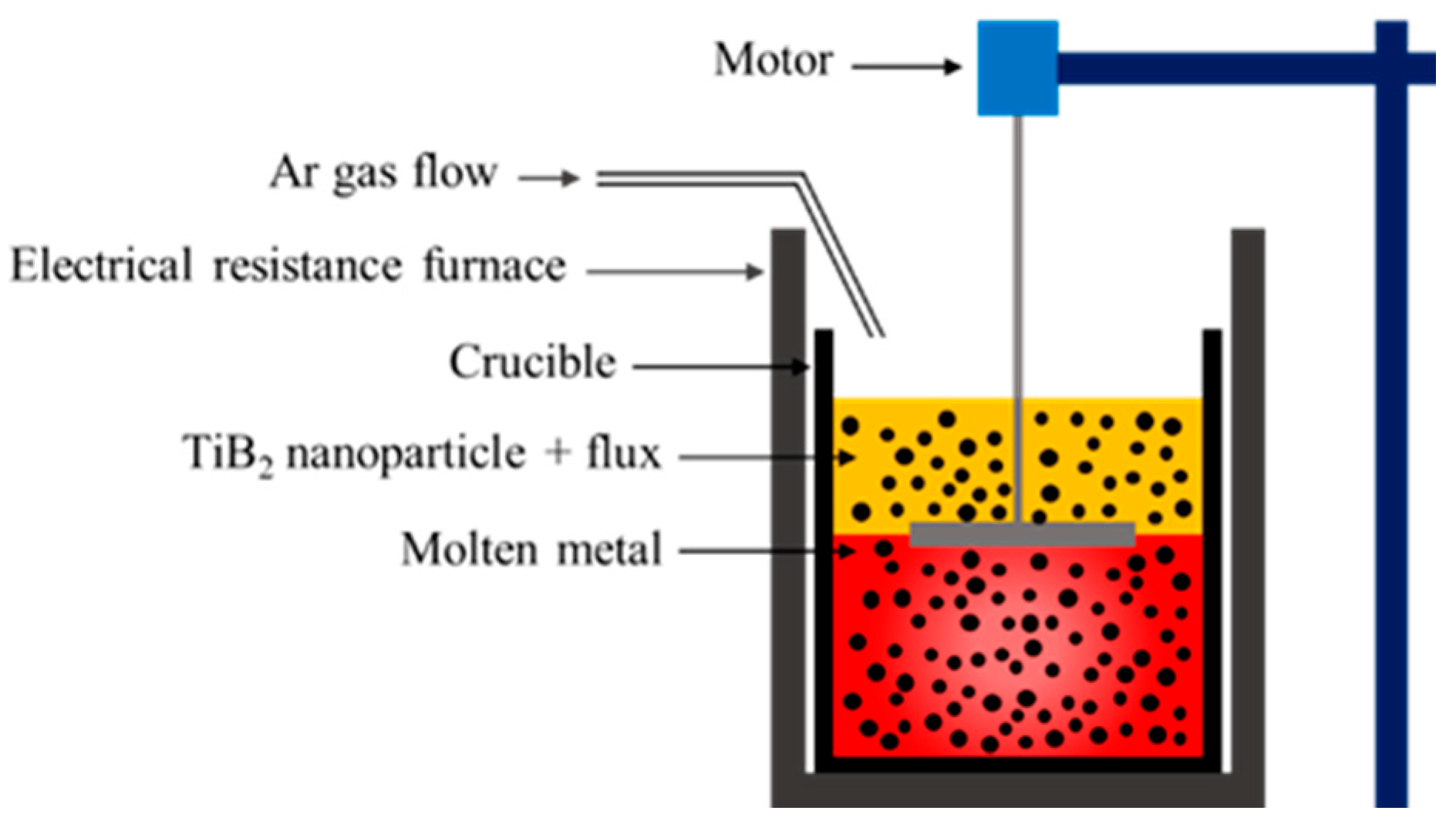
2. Materials and Methods

Materials synthesis. In this study, TiB2 was selected as the nano-reinforcement since it is an extremely hard ceramic. High-purity Al (99.99% purity, from American Elements Co. Ltd., Los Angeles, CA, USA) ingots and in-house-synthesized TiB2 nanoparticles with an average size less than 8 nm were used as the matrix and nano-reinforcement, respectively. [33] TiB2 nanoparticles and KAlF4 (with the purity >98%, from Domydo Co. Ltd., Hebei, China) flux were mechanically mixed in the solid state for 3 h. The mixed powders were dehydrated at 120 ºC for 1 h in a vacuum oven (NRTL Certified 25L 200C Vacuum Oven from MTI Corporation, Richmond, CA, USA). An electrical resistance furnace (115 volts, 860 watts from Thermcraft, Inc., Winston-Salem, NC, USA) was then used to melt the Al ingots isothermally at 850 ºC under argon (Ar) gas (from Airgas, Los Angeles, CA, USA) flow protection. The mixed powders were gradually added to the melt surface and the melt was mechanically stirred at 200 rpm for 10 min with a one-inch diameter titanium (Ti) mixing blade. The melt was naturally cooled down to room temperature under Ar gas protection. The final product was (in the shape of a disk with a 1.5-inch diameter and 1.0-inch height) carefully extracted from the graphite crucible (from Eforlife, USA via Amazon online purchase). Figure 1 shows the schematic of the experimental setup. Al–X vol.% TiB2 (X=3, 5, and 10) nanocomposites were produced (three study samples were prepared from the top, middle, and bottom of each nanocomposite sample).
Characterization. Scanning electron micrographs (SEM) were acquired using a ZEISS Supra 40VP field emission microscope (from CNSI, Los Angeles, CA, USA) operating at 10 kV, and the EDS mapping was conducted on the same machine. During the EDS element mapping, Al K and Ti K peaks were used for characterization. X-ray diffraction scanning was conducted on a Panalytical Pro XRD machine (from MIC Facilities, Los Angeles, CA, USA), with the scanning voltage of 45 KV and scanning current of 40 mA. The step speed was set to 1º/min. FIB machining and characterization were conducted on a Nova 600 FIB system (FEI) (from NanoLab Facilities, Los Angeles, California, USA). The microhardness was measured on an LM 800AT microhardness tester (by Leco Inc., St. Joseph, MI, USA). The loading was set to 200 gf with a dwelling time of 10 s. The microhardness results were taken as an average of 10 measurements for each point. Electrical conductivity was measured by CDE ResMap 178 4-Point Probe (from NanoLab Facilities, Los Angeles, CA, USA). The electrical conductivity results were taken as an average of 5 measurements.

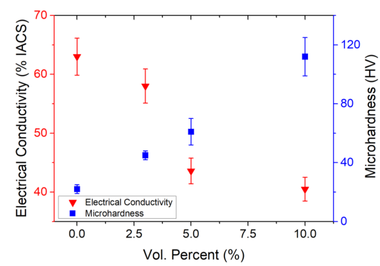
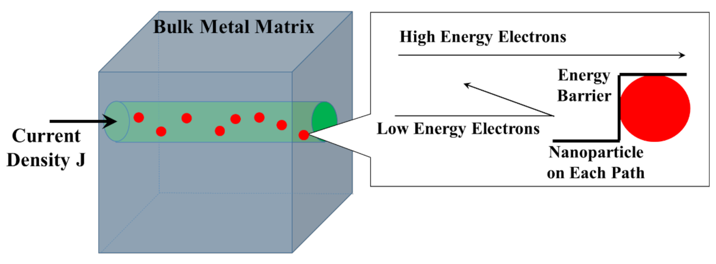
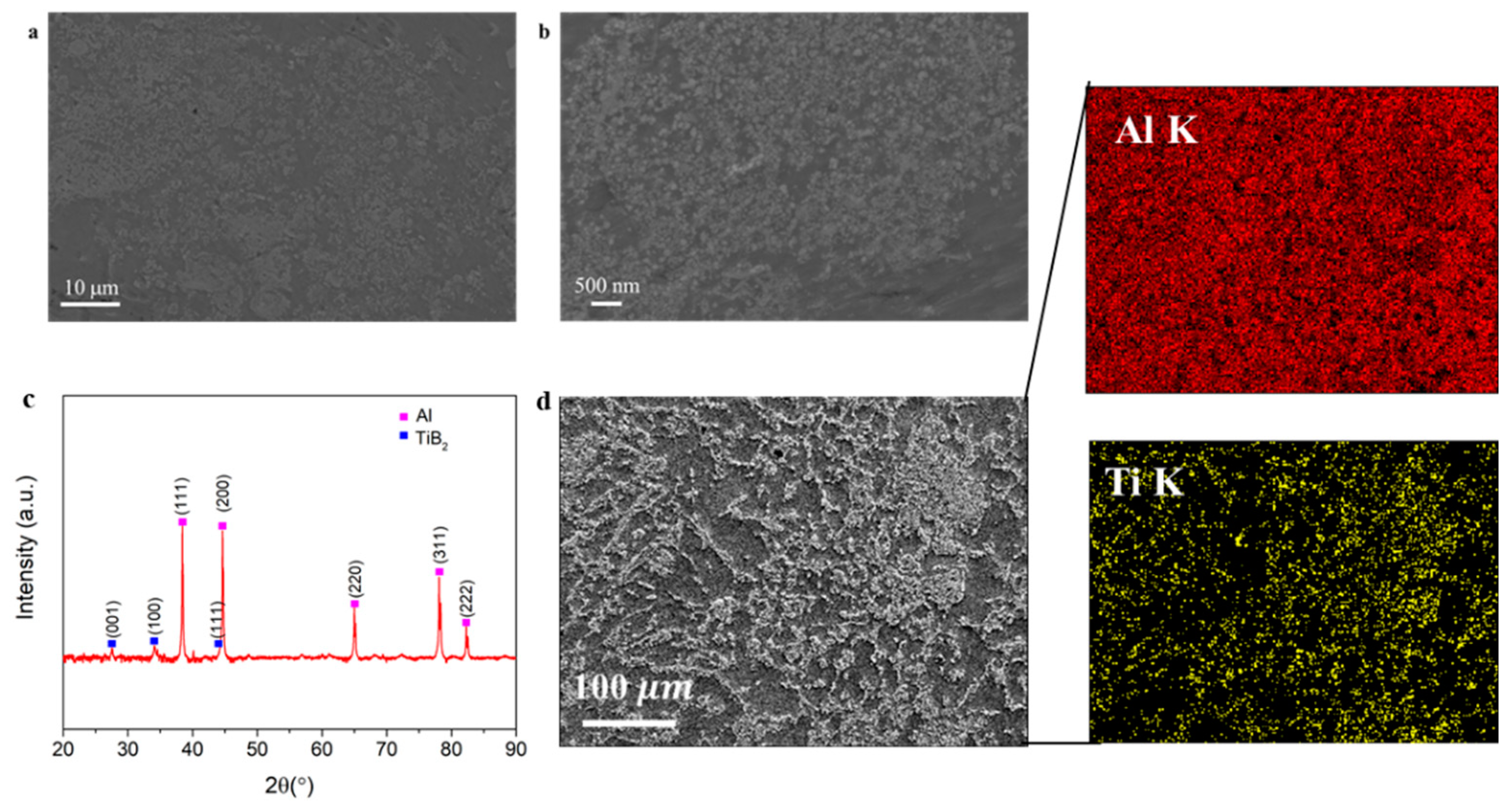
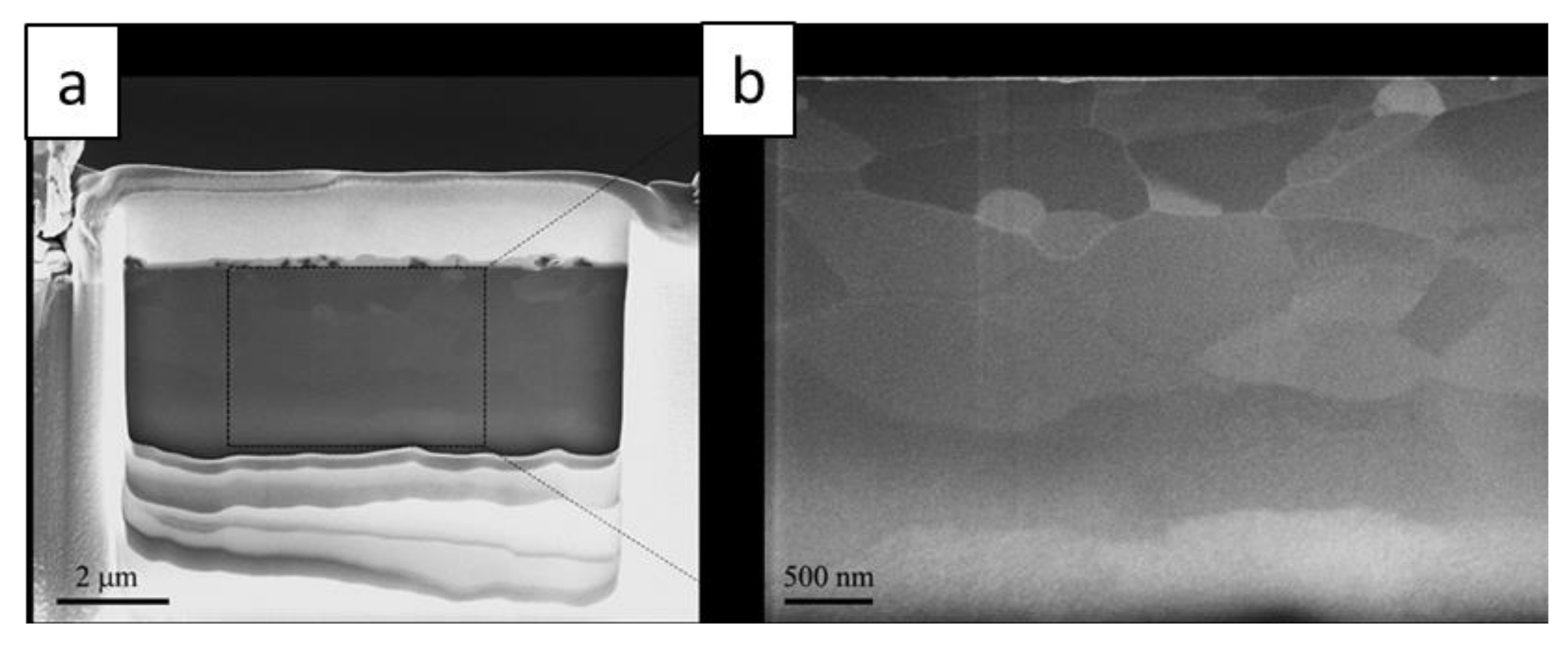
3. Results and Discussion

Figure 2 shows the Vickers hardness versus electrical conductivity (%IACS) result for pure Al as well as Al–TiB2 nanocomposites with three different volume concentrations of TiB2 nanoparticles Al matrix. The Vickers hardness and electrical conductivity of the as-cast pure Al were measured to be 25±3 HV and 63±3.5% IACS (2.8 μΩ.cm), which are set as the reference points for the Al–TiB2 system. Both the tests were carried out at room temperature (25 °C) with a constant humidity of about 38%. As the volume percent of the nanoparticles increased, the hardness of the Al nanocomposite became higher due to the addition of the hard TiB2 ceramic nanoparticles. On the other hand, TiB2 nanoparticles acting as electron scattering centers in the Al nanocomposite caused electrical conductivity reduction. With 3, 5, and 10 vol.% TiB2 in the aluminum matrix, the electrical conductivity of the nanocomposite samples was 58.0%, 43.6%, and 40.5% IACS, respectively. Compared with other similar Al alloy systems [1,3], our nanocomposites, even with over 3 vol.% TiB2, could offer a higher electrical conductivity, which demonstrates their advantages and great potential in electrical conductor applications.
Electrical conductivity. Classical electrical conductivity theory is based on the free electrons that move throughout the lattice of the metal. Considering Drude’s free electron theory [34], electrons are free to move in every direction within the metal lattice by following Newton’s laws of motion and Maxwell–Boltzmann statistics [35]. The electrical resistivity and electron mean-free path of a given metal are constant values. MFP is inversely proportional to the electron scattering probability. The electron’s interaction with the lattice and inclusion (defect) promotes electron scattering, consequently leading to increases in electrical resistivity. According to Matthiessen’s rule, the electrical resistivity of metals is the summation of two main parts: thermal ( ρ T ) and residual ( ρ R ). ρ T refers to the direct effect of environmental temperature on the electrons in the metal. The ρ R is associated with the microstructure of the metallic systems that contribute to electron scattering, such as lattice scattering, impurity scattering, precipitate scattering, and grain boundary scattering [36,37]. When comparing the conventional strengthening mechanism approaches, one can conclude that electron scattering and consequently electrical conductivity reduction are inevitable. For metals such as Al, the electrical conductivity analysis can be carried out with the Drude model under the expression:
S 0 = n τ e 2 m *
where S 0 indicates the matrix’s electrical conductivity without nanoparticle incorporation under the same temperature condition.   τ is the relaxation time of the free mobile electrons in the matrix, corresponding to MFP; e is the charge every electron carries; m * denotes the effective mass of the electrons. n is the number density of the electron, which is the key parameter to determine the electrical conductivity in our model. According to Nordheim’s rule [38,39], the electrical conductivity of the nanocomposites can be written as:
1 S = 1 S 0 + k 1 x 1 x + k 2 x
where S is the electrical conductivity of the nanocomposite,   k 1 represents the nanoparticle–metal interaction and   k 2 corresponds to the effects of the nanoparticles as a secondary phase in electrical conductivity. x is the nanoparticle volume fraction.
Figure 3 presents a schematic of the electrons pathway inside a metal matrix nanocomposite. The topographical impedance on the current density pathway will block the transport of electrons, as shown in Figure 3. At the macroscopic level, k 2 (~0.23505 uOhm–cm in our case) will be greater than k 1 (~0.00797 uOhm–cm in our case) (especially when x < 0.2 ). This is because the nanoparticles’ interaction with the matrix is negligible (both physically, such as the Gibbs free energy change, the interfacial energy change, and the phase transition energy, and chemically, such as the chemical reactions and the electronic structure’s tuning) [40]. As a result, the nanoparticle phase will play a dominant role in the electrical conductivity of the nanocomposite. Furthermore, the valences of the electrons are different in the metal Al and the ceramic TiB2, which leads to deviation from the approximate linearity of the electrical resistivity associated with k 2 x for the electrical conductivity and nanoparticles volume fraction, as shown in Figure 3.
Another important reason is the interfacial scattering along the metal and nanoparticle boundaries. This is supported by the sharp slope of change in the electrical conductivity in the nanocomposite samples with around 3 vol.% to 5 vol.% of TiB2 nanoparticles (Figure 1), which indicates that the interface must have played a more and more significant role when the incorporated nanoparticles reached a certain volume percent. In the case of higher volume fractions (~ 3 vol.% to 5 vol.%) of nanoparticles in the matrix, the transporting electrons have a greater chance of encountering the energy barrier between the metal matrix and nanoparticles. Therefore, the electrical conductivity drops more severely. This scattering is mainly due to the interfacial contact. Al and TiB2 have free electrons at different energy levels and different electronic band structures [40,41], and the interface of these two will present an energy difference that scatters the mobile electrons [41,42]. When lower-energy electrons encounter the Al–TiB2 interface, they will be scattered during transport, which reduces the electrical conductivity of the nanocomposite due to the band mismatch at the interface [40,42,43].
Since TiB2 acts as a second phase in the Al matrix and has mobile free electrons with different energy levels in different electronic structures, a decaying trend in the electrical conductivity is expected. However, even for an Al system with up to 10 vol.% TiB2, as in our case, about 43% IACS electrical conductivity is still very high, and it is thus suitable for many electrical applications.
Ultra-fine grain in the nanocomposite. We first characterized the distribution and dispersion of the TiB2 nanoparticles in an as-casted Al–TiB2 nanocomposite sample using scanning electron microscopy. To clearly reveal the nanoparticles, the SEM samples were cleaned via low-angle ion milling (10°, to remove the nanometer-sized polishing powders). SEM images of the Al–TiB2 nanocomposite are shown in Figure 4. Figure 4a shows the high volume fraction of the TiB2 nanoparticles uniformly dispersed and distributed in the aluminum matrix. Higher-magnification SEM images illustrate that the TiB2 nanoparticles retain their original size with any chemical sintering (Figure 4b).
A focused ion beam (FIB) was used to cut several aluminum nanocomposite samples. The bottom surface of the aluminum nanocomposite samples revealed a surprising phenomenon. The size of the grain in the as-cast aluminum nanocomposite sample reached ultra-fine grain size under a low cooling rate. The smallest grain size observed was about 300 nm. This unusual phenomenon is attributed to the presence of the nanoparticles acting both as nucleation sites and more importantly pinning down the growth of the aluminum grain, thus enabling it to obtain ultra-fine grain sizes. Figure 5a shows the thin cross-sectional sheet of aluminum nanocomposite milled via FIB. Figure 5b shows high-magnification SEM images clearly representing the nanosized aluminum grains attained in slow cooling.
Nanoparticle dispersion mechanism. In our nanoparticle–molten metal model system, nanoparticles are assumed to be uniformly distributed and dispersed in a molten metal (Figure 4). For simplicity, only interactions between two identical nanoparticles in a molten metal are considered. Figure 6 shows a schematic of two identical nanoparticles (e.g., TiB2) in a static molten metal (e.g., molten Al at 850 °C). For our model we assumed: (1) nanoparticles with a radius R are spherical in shape and D is the gap between two nanoparticles; (2) there was no macroscopic convection in the melt; (3) there was negligible electrostatic interaction or double layers between the nanoparticles and molten metal; (4) there were negligible buoyancy and gravity forces acting on the nanoparticles; (5) there was no severe chemical reaction between the nanoparticles and molten metal, and (6) there was no gas film or contamination on the nanoparticles’ surfaces.
Based on the above assumptions, three major interactions—interfacial energy, van der Waals potential, and Brownian potential—are considered in this model system.
When two nanoparticles interact in a molten metal far apart from each other, the interfacial energy is:
G b = 2 S p l σ p l
where S p l is the surface area of a nanoparticle and σ p l is the interfacial energy between the nanoparticle and molten metal. If the two nanoparticles travel toward each other to push all metal atoms out and create a void between them, the interfacial energy would be:
G b = 2 ( S p l S p p ) σ p l + 2 S p p σ p
where S p p and σ p are the effective contact area and the surface energy of the nanoparticle, respectively. If the two nanoparticles attain a sufficient adhesive contact to chemically bond (i.e., sintering starts), there will be no physical interface between the two nanoparticles. We consider this global energy minimum to be zero. Therefore, when two nanoparticles move close enough together to squeeze the metal atoms out and create a void between them, the change in Gibbs free energy can be described as:
Δ G 1 = 2 S σ p σ p l
where S is the effective contact area. If the nanoparticles move closer together to start chemically bonding with each other, the change in Gibbs free energy can be written as:
Δ G 2 = 2 S σ p
Since the interfacial energy is always positive, Δ G 2 would always be negative. Hence, the interaction potential of two similar surfaces of a unit area along with the gap between them, D , can be expressed as:
W i n t e r D = 2 S σ p σ p l   e D D 0 / a 0 D a 0 D 0 a 0 ,   f o r   ( D 0 < D < a 0 )
W i n t e r D = 2 S σ p e D / a 0 1 D / D 0 + 2 S σ p σ p l ,   f o r   ( 0 < D < D 0 )
where D 0 is the chemical length bond, and a 0 is the characteristic decaying length (0.2~0.4 nm) for the chemical bond.
The van der Waals potential between two nanoparticles in a molten metal is of a relatively long range (0.2−9 nm). Nanoparticles tend to attract each other due the attract force induced by van der Waals potential. The van der Waals potential for two identical spheres of radius R1 is determined by [44,45]:
W v d w D = A R 12 D
where A is the system’s Hamaker constant for the nanoparticles’ interactions in the molten metal. To estimate the Hamaker constant A, the below equation can be used:
A = A N P A L 2
where A N P is the Hamaker constant for the nanoparticle, and A L is the Hamaker constant for the metal. Therefore, the van der Waals potential can be written as:
W v d w D = A N P A L 2 12 D R
Since nanoparticles are very small in size, they are free to move randomly under thermal fluctuations. Thus, Brownian potential needs to be considered for these small nanoparticles. The equipartition theorem suggests that the kinetic energy/potential of the Brownian motion is in one dimension for one particle. Therefore, the Brownian motion energy for the two-nanoparticle system in on dimension is kT. For two nanoparticles in a molten metal at high temperatures, it may be comparable to the van der Waals potential, and thus the Brownian potential would play an important role in nanoparticle dispersion.
In the model system for nanoparticle dispersion in a molten metal, the van der Waals potential, interfacial energy, and Brownian potential intrinsically co-exist. The interfacial energy dominates when the gap between two nanoparticles becomes one or two atomic layers. The van der Waals interaction dominates outside this gap up to a great distance (up to 10 nm or more). Hence, three possible cases can be considered for nanoparticle dispersion in a molten metal: clusters, pseudo-dispersion, and self-dispersion. In this study we focus on the self-dispersion case.
Figure 7 shows the interaction potentials for nanoparticle self-dispersion in the molten metal. If Wbarrier is high (i.e., good wettability between the nanoparticle and the molten metal) and the van der Waals potential well is not deep, the Brownian potential, kT, cannot cause the nanoparticles to pass the barrier for any adhesive contact, although the nanoparticles would not be kinetically trapped either. This would allow the nanoparticles to move freely without forming a chemical bond to another nanoparticle in the molten metal, which is the so-called self-dispersion.
To further validate the self-dispersion model, the Al–TiB2 system was studied. The Hamaker constants for Al and TiB2 are 266zJ and 256zJ [44], respectively. The average size of the TiB2 nanoparticles is 10 nm. Equation (10) is effective only when two TiB2 nanoparticles interact in molten Al, where the D is about 0.4 nm [44]. Therefore, by inserting the values into Equation (10), we get: W v d w D = −4.2zJ (4.2 × 10⁻²¹ J). The thermal energy value at 820 °C would be 15.11 zJ, which is higher than the van der Waals interaction potential. The surface energies for liquid Al and solid TiB2 are 1.1 J/m2 [46] and 3.0 J/m2 [47], respectively, and the contact angle between Al and TiB2 is 80 degrees ( D 0 = 0.1 nm and a 0 = 0.4 nm) at the aforementioned temperature. The effective interaction area, S , is about 15.7 nm2. We can calculate the Wbarrier to be 6.8 × 10³ zJ. Since the Wbarrier is more than 500 times greater than the Brownian potential, there is little chance of the TiB2 nanoparticles overcoming the energy barrier and adhering to each other (forming a cluster). Therefore, we can conclude that TiB2 nanoparticles can self-disperse in molten Al. This is in good agreement with our experimental results shown in the result section.

4. Conclusions

In this work, we introduce a novel and scalable approach to produce a new class of aluminum electrical conductor for DC transmission lines. A suitable nanoparticle was identified to significantly improve the mechanical properties of the aluminum matrix while retaining reasonable electrical conductivity. Small TiB2 nanoparticles (less than 10 nm) were effectively incorporated into the aluminum matrix via flux assisted liquid processing. TiB2 nanoparticles were well dispersed and distributed in the aluminum matrix. Al–10 vol.% TiB2 ANEC was successfully produced to offer a Vickers hardness of 130 and an electrical conductivity of 41% IACS. An ultra-fine grain size was achieved in the as-cast samples of nanocomposites. Mechanical property enhancement can be associated with the presence of TiB2 nanoparticles throughout the aluminum matrix, and more importantly, with the formation of ultra-fine aluminum grains. With this understanding, further processing, including extrusion, could be easily applied to the developed Al nanocomposites in order to make the electrical wires. The corresponding degradation behavior and service performance of the Al nanocomposite-based wires should then be assessed. Together with the abovementioned future works, novel Al nanocomposites could be readily utilized in the electrical and electronic fields.

Author Contributions

Conceptualization, X.L. and A.J.; methodology, S.P.; formal analysis, S.P. and C.C.; investigation, S.P. and C.C.; resources, X.L.; data curation, S.P.; writing—original draft preparation, A.J.; writing—review and editing, S.P. and X.L.; supervision, X.L.; funding acquisition, X.L. All authors have read and agreed to the published version of the manuscript.

Funding

This research was funded by National Science Foundation, grant number 1639164.

Institutional Review Board Statement

Not applicable.

Informed Consent Statement

Not applicable.

Data Availability Statement

The data presented in this study are available on request from the corresponding author. The data are not publicly available due to the situation that it is part of ongoing research.

Acknowledgments

We would like to express our thanks to Jiaquan Xu and Jie Yuan (PhD student at UCLA) for their insightful discussion on the theoretical part.

Conflicts of Interest

The authors declare no conflict of interest.

References

  1. Karabay, S. Modification of AA-6201 alloy for manufacturing of high conductivity and extra high conductivity wires with property of high tensile stress after artificial aging heat treatment for all-aluminium alloy conductors. Mater. Des. 2006, 27, 821–832. [Google Scholar] [CrossRef]
  2. Karabay, S. Influence of AlB2 compound on elimination of incoherent precipitation in artificial aging of wires drawn from redraw rod extruded from billets cast of alloy AA-6101 by vertical direct chill casting. Mater. Des. 2008, 29, 1364–1375. [Google Scholar] [CrossRef]
  3. Sauvage, X.; Bobruk, E.V.; Murashkin, M.Y.; Nasedkina, Y.; Enikeev, N.A.; Valiev, R.Z. Optimization of electrical conductivity and strength combination by structure design at the nanoscale in Al–Mg–Si alloys. Acta Mater. 2015, 98, 355–366. [Google Scholar] [CrossRef]
  4. Valiev, R.Z.; Murashkin, M.Y.; Sabirov, I. A nanostructural design to produce high-strength Al alloys with enhanced electrical conductivity. Scr. Mater. 2014, 76, 13–16. [Google Scholar] [CrossRef]
  5. Tian, L.; Anderson, I.; Riedemann, T.; Russell, A.; Kim, H. Prospects for novel deformation processed Al/Ca composite conductors for overhead high voltage direct current (HVDC) power transmission. Electr. Power Syst. Res. 2013, 105, 105–114. [Google Scholar] [CrossRef]
  6. Hou, J.P.; Wang, Q.; Yang, H.J.; Wu, X.M.; Li, C.H.; Li, X.W.; Zhang, Z.F. Microstructure evolution and strengthening mechanisms of cold-drawn commercially pure aluminum wire. Mater. Sci. Eng. A 2015, 639, 103–106. [Google Scholar] [CrossRef]
  7. Rhee, H.; Whittington, W.R.; Oppedal, A.L.; Sherif, A.R.; King, R.L.; Kim, H.J.; Lee, C. Mechanical properties of novel aluminum metal matrix metallic composites: Application to overhead conductors. Mater. Des. 2015, 88, 16–21. [Google Scholar] [CrossRef]
  8. How Much Electricity Is Lost in Transmission and Distribution in the United States? Available online: https://www.eia.gov/tools/faqs/faq.php?id=105&t=3 (accessed on 4 November 2017).
  9. Cabibbo, M. Microstructure strengthening mechanisms in different equal channel angular pressed aluminum alloys. Mater. Sci. Eng. A 2013, 560, 413–432. [Google Scholar] [CrossRef]
  10. Ding, S.X.; Lee, W.T.; Chang, C.P.; Chang, L.W.; Kao, P.W. Improvement of strength of magnesium alloy processed by equal channel angular extrusion. Scr. Mater. 2008, 59, 1006–1009. [Google Scholar] [CrossRef]
  11. Kim, W.J.; Wang, J.Y. Microstructure of the post-ECAP aging processed 6061 Al alloys. Mater. Sci. Eng. A 2007, 464, 23–27. [Google Scholar] [CrossRef]
  12. Chinh, N.Q.; Gubicza, J.; Langdon, T.G. Characteristics of face-centered cubic metals processed by equal-channel angular pressing. J. Mater. Sci. 2007, 42, 1594–1605. [Google Scholar] [CrossRef] [Green Version]
  13. Ito, Y.; Horita, Z. Microstructural evolution in pure aluminum processed by high-pressure torsion. Mater. Sci. Eng. A 2009, 503, 32–36. [Google Scholar] [CrossRef]
  14. Zhilyaev, A.P.; Langdon, T.G. Using high-pressure torsion for metal processing: Fundamentals and applications. Prog. Mater. Sci. 2008, 53, 893–979. [Google Scholar] [CrossRef]
  15. Sakai, G.; Horita, Z.; Langdon, T.G. Grain refinement and superplasticity in an aluminum alloy processed by high-pressure torsion. Mater. Sci. Eng. A 2005, 393, 344–351. [Google Scholar] [CrossRef]
  16. Kamikawa, N.; Huang, X.; Tsuji, N.; Hansen, N. Strengthening mechanisms in nanostructured high-purity aluminium deformed to high strain and annealed. Acta Mater. 2009, 57, 4198–4208. [Google Scholar] [CrossRef]
  17. Russell, A.M.; Chumbley, L.S.; Tian, Y. Deformation processed metal–metal composites. Adv. Eng. Mater. 2000, 2, 11–22. [Google Scholar] [CrossRef]
  18. Saito, Y.; Utsunomiya, H.; Tsuji, N.; Sakai, T. Novel ultra-high straining process for bulk materials—development of the accumulative roll-bonding (ARB) process. Acta Mater. 1999, 47, 579–583. [Google Scholar] [CrossRef]
  19. Pan, S.; Yao, G.; Yuan, J.; Sokoluk, M.; Li, X. Manufacturing of Bulk Al-12Zn-3.7 Mg-1Cu Alloy with TiC Nanoparticles. Procedia Manuf. 2020, 48, 325–331. [Google Scholar] [CrossRef]
  20. Yuan, J.; Zuo, M.; Sokoluk, M.; Yao, G.; Pan, S.; Li, X. Nanotreating High-Zinc Al–Zn–Mg–Cu Alloy by TiC Nanoparticles. In Light Metals; Springer: Cham, Switzerland, 2020; pp. 318–323. [Google Scholar]
  21. Fribourg, G.; Bréchet, Y.; Deschamps, A.; Simar, A. Microstructure-based modelling of isotropic and kinematic strain hardening in a precipitation-hardened aluminium alloy. Acta Mater. 2011, 59, 3621–3635. [Google Scholar] [CrossRef]
  22. Gupta, A.K.; Lloyd, D.J.; Court, S.A. Precipitation hardening in Al–Mg–Si alloys with and without excess Si. Mater. Sci. Eng. A 2001, 316, 11–17. [Google Scholar] [CrossRef]
  23. Carlton, C.E.; Ferreira, P.J. What is behind the inverse Hall–Petch effect in nanocrystalline materials? Acta Mater. 2007, 55, 3749–3756. [Google Scholar] [CrossRef]
  24. Pan, S.; Sokoluk, M.; Cao, C.; Guan, Z.; Li, X. Facile fabrication and enhanced properties of Cu-40 wt% Zn/WC nanocomposite. J. Alloys Compd. 2019, 784, 237–243. [Google Scholar] [CrossRef]
  25. Seidman, D.N.; Marquis, E.A.; Dunand, D.C. Precipitation strengthening at ambient and elevated temperatures of heat-treatable Al (Sc) alloys. Acta Mater. 2002, 50, 4021–4035. [Google Scholar] [CrossRef]
  26. Thieme, C.L.H.; Pourrahimi, S.; Foner, S. High strength Al metal-matrix microcomposite wire with 20 vol% Nb and ultimate tensile strengths up to 1030 MPa. Scr. Metall. Mater. 1993, 28, 913–918. [Google Scholar] [CrossRef]
  27. Russell, A.M.; Lund, T.; Chumbley, L.S.; Laabs, F.A.; Keehner, L.L.; Harringa, J.L. A high-strength, high-conductivity Al–Ti deformation processed metal metal matrix composite. Compos. Part A Appl. Sci. Manuf. 1999, 30, 239–247. [Google Scholar] [CrossRef]
  28. Xu, K.; Russell, A.M.; Chumbley, L.S.; Laabs, F.C.; Gantovnik, V.B.; Tian, Y. Characterization of strength and microstructure in deformation processed Al-Mg composites. J. Mater. Sci. 1999, 34, 5955–5959. [Google Scholar] [CrossRef]
  29. Hernandez, O.; Gonzalez, G. Microstructural and mechanical behavior of highly deformed Al–Sn alloys. Mater. Charact. 2008, 59, 534–541. [Google Scholar] [CrossRef]
  30. Chen, L.Y.; Xu, J.Q.; Choi, H.; Pozuelo, M.; Ma, X.; Bhowmick, S.; Yang, J.M.; Mathaudhu, S.; Li, X.C. Processing and properties of magnesium containing a dense uniform dispersion of nanoparticles. Nature 2015, 528, 539–543. [Google Scholar] [CrossRef] [PubMed]
  31. Pan, S.; Yuan, J.; Zheng, T.; She, Z.; Li, X. Interfacial thermal conductance of in situ aluminum-matrix nanocomposites. J. Mater. Sci. 2021, 56, 13646–13658. [Google Scholar] [CrossRef]
  32. Pan, S.; Guan, Z.; Li, X. Unusual thermal performance in Cu-60Ag by WC nanoparticles. Mater. Sci. Eng. B 2021, 265, 115010. [Google Scholar] [CrossRef]
  33. Yuan, J.; Yao, G.; Pan, S.; Murali, N.; Li, X. Size Control of In Situ Synthesized TiB 2 Particles in Molten Aluminum. Metall. Mater. Trans. A 2021, 52, 2657–2666. [Google Scholar] [CrossRef]
  34. Drude, P. The Theory of Optics; Courier Dover Publications: New York, NY, USA, 1901. [Google Scholar]
  35. Gao, W.; Sammes, N.M. An Introduction to Electronic and Ionic Materials; World Scientific Publishin Co. Inc.: Singapore, 1999. [Google Scholar]
  36. Andrews, P.V.; West, M.B.; Robeson, C.R. The effect of grain boundaries on the electrical resistivity of polycrystalline copper and aluminium. Philos. Mag. 1969, 19, 887–898. [Google Scholar] [CrossRef]
  37. Miyajima, Y.; Komatsu, S.Y.; Mitsuhara, M.; Hata, S.; Nakashima, H.; Tsuji, N. Change in electrical resistivity of commercial purity aluminium severely plastic deformed. Philos. Mag. 2010, 90, 4475–4488. [Google Scholar] [CrossRef]
  38. Friedel, J. On some electrical and magnetic properties of metallic solid solutions. Can. J. Phys. 1956, 34, 1190–1211. [Google Scholar] [CrossRef]
  39. Nordheim, V. Zur theorie der Elektronen in Metallen. Ann. Phys. 1931, 5, 642. [Google Scholar]
  40. Kittel, C.; Kroemer, H. Thermal Physics, 2nd ed.; AAPT: Sydney, Australia, 1998. [Google Scholar]
  41. Pan, S.; Yuan, J.; Zhang, P.; Sokoluk, M.; Yao, G.; Li, X. Effect of electron concentration on electrical conductivity in in situ Al-TiB2 nanocomposites. Appl. Phys. Lett. 2020, 116, 014102. [Google Scholar] [CrossRef]
  42. Pan, S.; Guan, Z.; Yao, G.; Cao, C.; Li, X. Study on electrical behaviour of copper and its alloys containing dispersed nanoparticles. Curr. Appl. Phys. 2019, 19, 452–457. [Google Scholar] [CrossRef]
  43. Pan, S.; Yao, G.; Yuan, J.; Li, X. Electrical Performance of Bulk Al–ZrB 2 Nanocomposites from 2 K to 300 K. In Nanocomposites VI: Nanoscience and Nanotechnology in Advanced Composites; Springer: Cham, Switzerland, 2019; pp. 63–70. [Google Scholar]
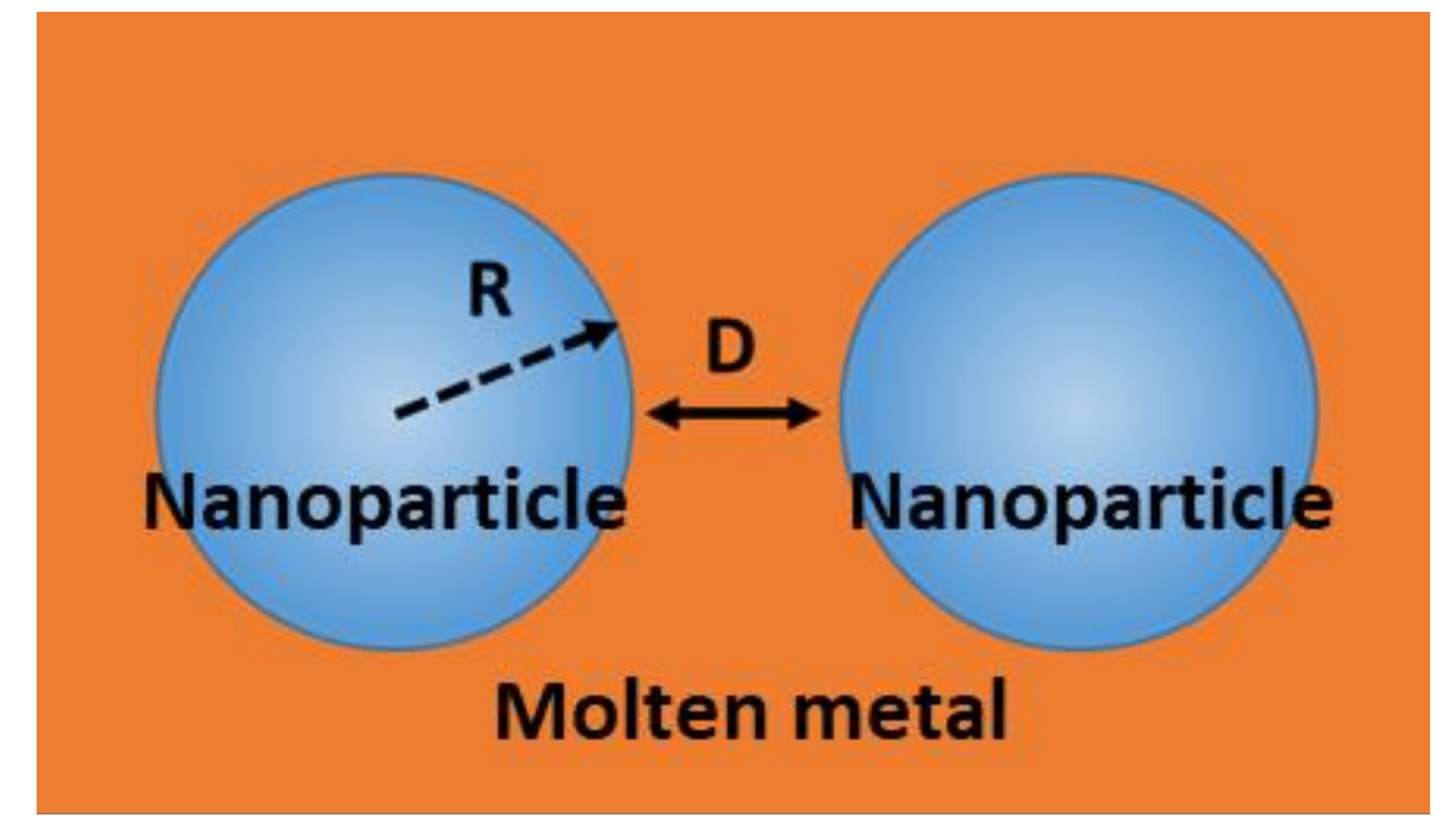
  44. Israelachvili, J.N. Intermolecular and Surface Forces; Academic Press: Cambridge, MA, USA, 2011. [Google Scholar]
  45. Hamaker, H. The London—van der Waals attraction between spherical particles. Physica 1937, 4, 1058–1072. [Google Scholar] [CrossRef]
  46. Rhee, S.K. Wetting of AlN and TiC by liquid Ag and liquid Cu. J. Am. Ceram. Soc. 1970, 53, 639–641. [Google Scholar] [CrossRef]
  47. Cook, B.A.; Russell, A.M.; Peters, J.; Harringa, J.L. Estimation of surface energy and bonding between AlMgB14 and TiB2. J. Phys. Chem. Solids 2010, 71, 824–826. [Google Scholar] [CrossRef]
Figure 1. Schematic of the flux-assisted liquid state processing experimental setup.
Jcs 05 00172 g001
Figure 2. Effect of TiB2 nanoparticles on mechanical and electrical properties of Al–TiB2 nanocomposites.
Jcs 05 00172 g002
Figure 3. The schematic illustration of the scattering mechanisms in the Al–TiB2 nanocomposite system (the left side indicates the structural impedance caused by nanoparticle incorporation, whereas the right side demonstrates the interfacial energy barrier formed by Al and TiB2).
Jcs 05 00172 g003
Figure 4. Electron microscopy study. (a) SEM images of the Al–TiB2 nanocomposite samples. (b) Higher-magnification SEM images obtained from the Al–TiB2 nanocomposites. (c) XRD scanning results to confirm the phases in Al–TiB2 (Al–3 vol.% TiB2 as an example). (d) EDS mapping for the Al–TiB2 nanocomposites (Al–5 vol.% TiB2 as an example) after ion milling to expose the TiB2 zone.
Jcs 05 00172 g004
Figure 5. Focused ion beam. (a) Aluminum–TiB2 nanocomposite sample sheet prepared by FIB. (b) High-magnification SEM images obtain from the rectangular box (from a) vividly showing the ultra-fine-grain aluminum.
Jcs 05 00172 g005
Figure 6. Model for two identical nanoparticles interacting in a molten metal.
Jcs 05 00172 g006
Figure 7. Interaction potentials for nanoparticle self-dispersion in molten metal with an inset to show how nanoparticles disperse in molten metal.
Jcs 05 00172 g007
Publisher’s Note: MDPI stays neutral with regard to jurisdictional claims in published maps and institutional affiliations.

