Article

Fabrication of an Optically Transparent Planar Inverted-F Antenna Using PEDOT-Based Silver Nanowire Clear Ink with Aerosol-Jet Printing Method towards Effective Antennas

1
Laboratory for Physical Sciences, College Park, MD 20740, USA
2
Electrical and Computer Engineering Department, University of Maryland, College Park, MD 20742, USA
*
Author to whom correspondence should be addressed.
J. Manuf. Mater. Process. 2024, 8(1), 39; https://doi.org/10.3390/jmmp8010039
Submission received: 12 December 2023 / Revised: 5 February 2024 / Accepted: 7 February 2024 / Published: 10 February 2024

Abstract

:
We report the design, fabrication, and experimental characterization of an optically transparent printed planar inverted-F antenna (PIFA) operating at 2.45 GHz using the aerosol jet (AJ) printing method. The proposed antenna was fabricated using a clear conductive ink on glass and Delrin. The antenna exhibits a wide fractional bandwidth (FBW) of 20% centered at 2.45 GHz, with a peak realized gain of −3.6 dBi and transparency of ~80%. The proposed fabrication method provides a cost-effective and scalable solution for manufacturing transparent antennas with potential applications in wireless communication, sensing, and wearable devices operating at mmWave frequencies higher than 30 GHz.

1. Introduction

The conventional methods for fabricating electronic parts such as PCBs and antennas involve the use of significant amounts of chemicals to etch a copper film onto plastic substrates in order to create circuit patterns. The process that is currently being used results in a considerable amount of environmental pollution, which can have a harmful impact on the ecosystem and human health [1]. Some of the advantages of 3D-printed antennas, unlike traditional antennas, include being relatively pollution-free, rapid prototyping, and a simple fabrication process. Transparent antennas have attracted significant attention due to their potential applications in various fields, such as wireless communication, sensing, and wearable devices [2,3].
Recently, there has been a significant surge in the exploration of transparent antenna fabrication, captivating the attention and efforts of a multitude of researchers. As listed in Table 1. Wu et al. developed a transparent conducting film using an Aluminum Zinc Oxide (AZO)/Ag Nano Wires (AgNWs) composite and built a wide-band transparent antenna for Bluetooth communication using the RF magnetron sputtering deposition method [4]. Using a similar deposition method, Zamudio et al. demonstrated the feasibility of using AZO as a transparent and conductive material for Optically Transparent Antenna (OTA) fabrication, which can be integrated with photovoltaics for a high efficiency [5]. Peter et al. presented a transparent ultra-wideband antenna that can be integrated with photovoltaic solar panels, harvest RF energy, and operate in the frequency range from 2.2 to 12.1 GHz [6].
Sheikh et al. investigated a transparent microstrip antenna with a fluorine-doped tin oxide patch, deposited using a spray pyrolysis technique on a Pyrex glass substrate, demonstrating high optical transmittance and low electrical surface resistance, and they compared the radiation properties with copper patch antenna counterparts [7]. The paper by Erfeng et al. presents a flexible and transparent ultrawideband (UWB) antenna that uses a transparent conductive fabric tissue on a polydimethylsiloxane (PDMS) substrate, with promising potential for future wireless networks [8]. Malek et al. proposed a dual-band transparent antenna for active RFID tags operating at 2.4 GHz and 5.8 GHz, using a AgHT-8 thin film with a high transparency above 80%, allowing for easy lamination on the surface of tag devices with little chance of detection, and achieving a high FBW [9].
As stated above, common transparent conductive materials include Indium Tin Oxide (ITO), Zinc Oxide (ZnO), Aluminum-doped Zinc Oxide (AZO), and Graphene. These materials exhibit high electrical conductivities, with ITO and Graphene typically reaching around 104 S/m, while ZnO and AZO have conductivities around 103 S/m.
While various fabrication methods have been proposed so far, there is currently no existing study on the printing of transparent antennas using the AJ printing method as shown in Figure 1. In this paper, we introduce an optically transparent printed planar inverted-F antenna (PIFA) designed for operation at the frequency of 2.4 GHz (WiFi), fabricated using the AJ method. We used a clear conductive ink containing PEDOT:PSS polymer, silver nanowires (NW), high boiling solvents, and surfactants on two different substrates, namely, glass and Delrin. The ~1 micron-thick conductive film used for printing was found to have an optical transparency of over 50% at the wavelength of 632 nm, as measured through a simple transmission test (details in Section 3.1). The trade-off between transparency and antenna gain may limit the potential applications of transparent antennas. High transparency typically results in increased resistance and reduced antenna gain, but this feature also makes the antenna suitable for use in applications where transparency is a critical requirement. The results show that the fabricated antennas have good impedance matching and reasonable bandwidth, indicating their potential for use in various applications. This AJ printing method offers a rapid, cost-effective, and scalable solution for manufacturing transparent antennas with potential applications in wireless communication, sensing, and wearable devices operating at mmWave frequencies higher than 30 GHz, thanks to the high resolution achievable with the AJ printing method.

2. Materials and Methods

Historically, traditional electronic circuits have been fabricated on flat and rigid substrates. Recent advances in additive manufacturing capabilities are bringing new ways for electronic circuits and devices to be fabricated. One new type of additive manufacturing method that has gained traction in recent years is known as direct-write printing. Direct-write prints allow for features in the design file to be directly printed onto the substrate without the need for first depositing and removing excess material. Of the direct-write printing methods, aerosol jet (AJ) printing offers distinct advantages such as being able to print with a standoff 2–5 mm above the substrate as well as printing ink stream widths down to 15 to 20 microns [10,11]. This advantage allows for printing on non-flat surfaces as well as surfaces with complex topographies.
AJ printing uses the principle of aerosolization of functional inks to create circuitry. The functional inks are aerosolized using two methods: pneumatic and ultrasonic aerosolization. Once aerosolized, these ink droplets are carried through a series of multi-stage focusing orifices and finally jetted out from a nozzle. When equipped with a wide feature nozzle, it is capable of printing large ink-stream widths upwards of 1 mm in diameter, making it a versatile tool for printing small, intricate features as well as large areas. Applications of small-ink stream resolutions include the fabrication of high-density interconnects, the ability to connect high density pads on bare die, as well as many others.
The AJ system can also be configured to allow for 5-axis printing. This is performed by mounting the part to a 2-axis trunnion, which, in addition to the traditional 3-axis (x, y, and z) directions, adds the a-axis and c-axis of rotations. This 5-axis toolpath is created in CAD/CAM software such as Creo parametric 10.0 or MasterCAM 2022 and then loaded on the tool. With this capability, many complex geometries and features can be created on demand. One such example is printing conductive windings on an inductor core. Currently, there are continuing efforts to improve the state-of-the-art of AJ printing and direct-write printing methods. Improving the ink stream stability of the tool, developing new inks for printing, and enhancing the resolution limit of printing are just a few examples.
Figure 2 shows a picture of the AJ tool (AJ5X), which is capable of printing in five axes. In order to enhance the capability of the tool, we made custom configurations to the tool. This includes the ring mount, which features a dovetail design, allowing for additional components to be mounted around the print head. Using this dovetail feature, we added a UV light that can be controlled directly in the toolpath, allowing for UV active materials to be cured in situ. In addition, an inkwell stand was secured to the side of the trunnion to allow for deposition rate measurements before and during the printing process [12].
The clear conductive ink for this research was developed by Heraues. In particular, we chose the Clevios HY Jet 2, developed specifically for inkjet printers and printed electronic applications [13]. This ink is an aqueous dispersion containing PEDOT:PSS polymer, silver nanowires, high boiling solvents, and surfactants. The ink, with a viscosity of 11 cP, is slightly high for an ultrasonic atomizer, but it is suitable for printing using the pneumatic AJ printer as it was manufactured. The optical transmission is 85.8%, and the solid loading is 0.77%. When not in use, this ink is stored between 15 and 25 degrees Celsius. Before loading on the printer, the ink is rolled on a roller for 15 min.
The surface preparation of the substrate before printing is necessary for creating good adhesion of Clevios HY Jet 2. Several surface preparation steps were taken to ensure proper adhesion when fabricating the antenna. First, the substrate was lightly sanded down with fine-grit sandpaper. Next, the substrate was sonicated in an ultrasonic bath with deionized water for 10 min, followed by isopropyl alcohol for 10 min. After rinsing off the solvents, the substrate was placed in a UV ozone chamber for 15 min to remove organic contaminants.
Prior to printing, the ink should be rolled on a roller for 30 min. If the ink has not been used for long periods of time, a planetary mixer is recommended. The value of 2000 rpm for 1 min is a typical value used on our planetary mixer. When not in use, the ink should be stored in an inert environment to preserve the shelf life of the ink. The ink itself is ready to be atomized using the pneumatic atomizer. No dilution is necessary. If seeking to use the ultrasonic atomizer, additional solvent could be added to dilute the ink to a lower viscosity. This was not attempted in our experiment.
Clevios HY Jet 2 poses some challenges on the pneumatic print head. Due to the presence of surfactants, the ink tends to foam after being atomized. Additionally, the silver nanowires in the ink agglomerate at the nozzle and clog the nozzle after about one hour of printing. To remediate these issues, decrease the total flow rate through the nozzle and increase the sheath gas flow rates to protect the nozzle. Typical values when printing were 33 sccm for the sheath, 700 sccm for the atomizer, and 680 sccm for the exhaust. For long prints of more than 2 h, the mist tube needs to be changed out to prevent clogging in the tube.
At the start of the printing, the ink stream requires a certain amount of time for the ink stream to stabilize. This is called the burn-in time for the ink. The Clevios HY Jet 2 requires about 8 min of burn-in time for stabilization. During this time, the ink stream evolves from a thin line of about 40 microns wide to a much wider ink stream of about 100 microns. After the burn-in period, the ink stream is ready to be tuned. Each type of ink tunes slightly differently depending on the amount of high-boiling and low-boiling solvents in the ink. It may also vary if the ink is formulated with additional additives. For the HY Jet 2, once the burn-in period is complete, the ink needs to be tuned down by decreasing the differential between the atomizer and exhaust flow rates. A typical differential for the HY Jet 2 is about 40 sccm. Holding the differential constant, both the atomizer and exhaust gas flows can be decreased at increments of 30 sccm until the desired ink stream width is achieved. One other parameter that can be adjusted for higher printability of the ink is the print speed. HY Jet 2 tends to print in a wetter way, oftentimes spilling into neighboring areas that are undesired. This gives the illusion that there may be a clogged nozzle or occurrence of unstable atomization. If this occurs, keep the atomizer and exhaust flow rates at higher values and increase the print speed to 3 or 4 mm/s. Check the ink stream profile by printing onto a scrap substrate moving around horizontally and vertically. The optimal print speed for this ink is between 2 and 5 mm/s. There are minimal amounts of overspray produced by this ink, but in general, 10% overspray should be accounted for when designing for minimum pitch spacing.
When printing on lower-surface-energy substrates, the silver nanowires in the HY Jet 2 will agglomerate, causing ripples in the print. This, in turn, will affect the conductivity of the final print. To mitigate this issue, each layer in the print is alternated between vertical and horizontal rastering to form a hash. This hash structure increases the overlap between the silver nanowires and allows for the conductivity to be maintained. Once the printing is complete, the sample should be cured in an inert environment to prevent oxidation of the silver nanowires. The curing profile used in this experiment was 150 °C for 3 h in a nitrogen-filled oven. Allow the sample to cool down to room temperature naturally. To pre-vent further oxidation of the clear ink in air after curing, an encapsulation layer can be applied. The encapsulation material should ideally be optically transparent and not significantly alter the dielectric properties of the active device.
To provide a better contact to the SMA connector, silver contact pads are printed as an additional layer directly on the clear ink. The pads are designed to match the spacing of the SMA connector, with a silver pad printed on either side of the signal line at the feed-in. The silver pads are printed using Dowa silver nanoparticle ink and processed in the same manner as documented in previous papers. A total of 6 layers are printed for a total thickness of about 25 microns. In addition to providing better contact to the SMA, the silver pads also prevent the SMA pins from directly contacting the printed clear ink, which may cause scratching or delamination of the clear ink from the substrate.
Basic ink characterization was performed on Clevios HY Jet 2 to determine the printing parameters as well as the fundamental ink properties, including thickness per layer, resistivity, and optical transparency. To perform this, dog bone structures with increasing number of layers were printed on a glass slide. A total of 1~5 layers were printed and cured in the oven at 130 °C for an hour. The post-cured samples were measured in a stylus profilometer, and the thickness per layer was measured to be 0.12 μm/layer. The resistivity was determined to be 8.4 × 10⁻⁶ Ω·m. As shown in Figure 3, optical transparency decreased with increasing number of layers.
The first antenna was designed to be printed on a glass substrate. The type of antenna is a PIFA with coplanar feed in structure. The important parameters for printing and fabrication are detailed in Table 2. The feed coplanar waveguide (CPW) was designed to be impedance-matched to 50 ohms. The size of the glass substrate was 25 × 75 × 1 mm3. An edge launch SMA connector was attached at the feed-in point. The dielectric constant of the glass slide was experimentally determined by fabricating a ground coupled microstrip line using copper tape. The S11 reflection patterns were matched in an HFSS simulation, and the dielectric constant was tuned until the free spectral range was closely matched near the 2.4 GHz region. Using this method, the dielectric constant of the glass slide was determined to be 4.7. This value was then fed into the HFSS design to simulate the PIFA antenna. The loss tangent was not measured because it was not expected to have much impact on the antenna design. The resulting relevant dimensions of the PIFA are provided in Table 3.
For this antenna design, we chose to print 10 passes in order to achieve a thick-enough layer for good adhesion as well as a resistance that would yield sufficient gain. We printed first on a glass substrate to demonstrate the transparency of the ink. A second antenna was printed on Delrin substrate. This was also printed with 10 passes. For the CI/glass sample, the optical transparency was measured to be approximately 50%, and the printed film had a sheet resistance of around 4 Ω/sq.

3. Simulation and Results

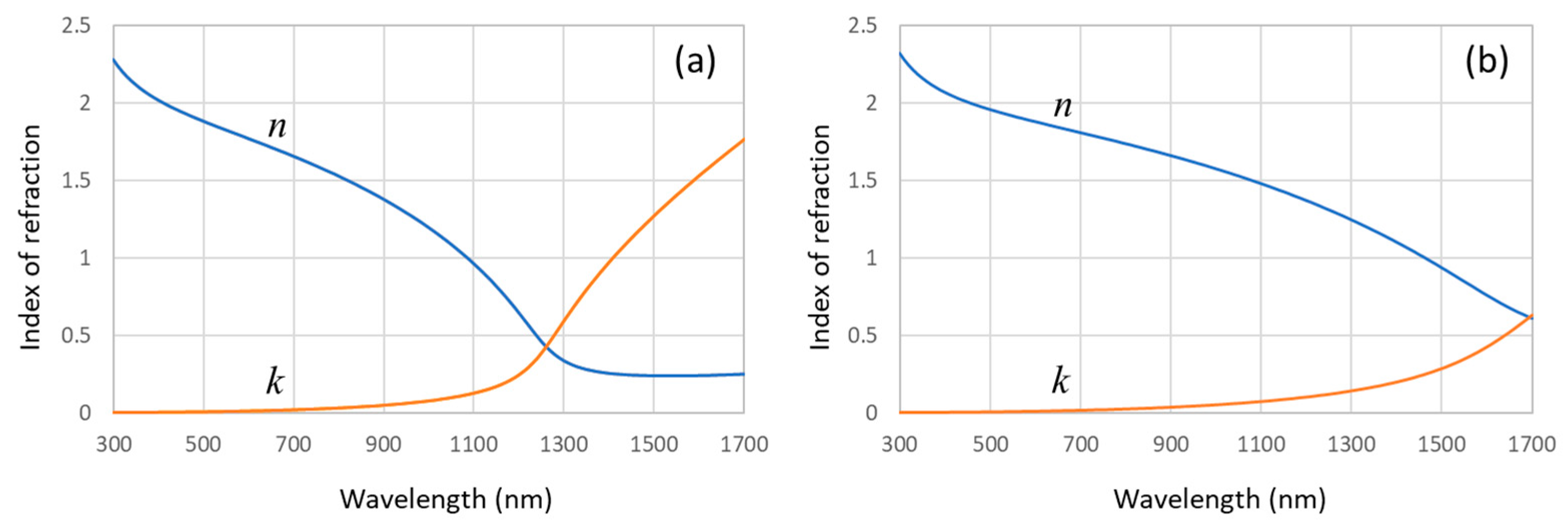
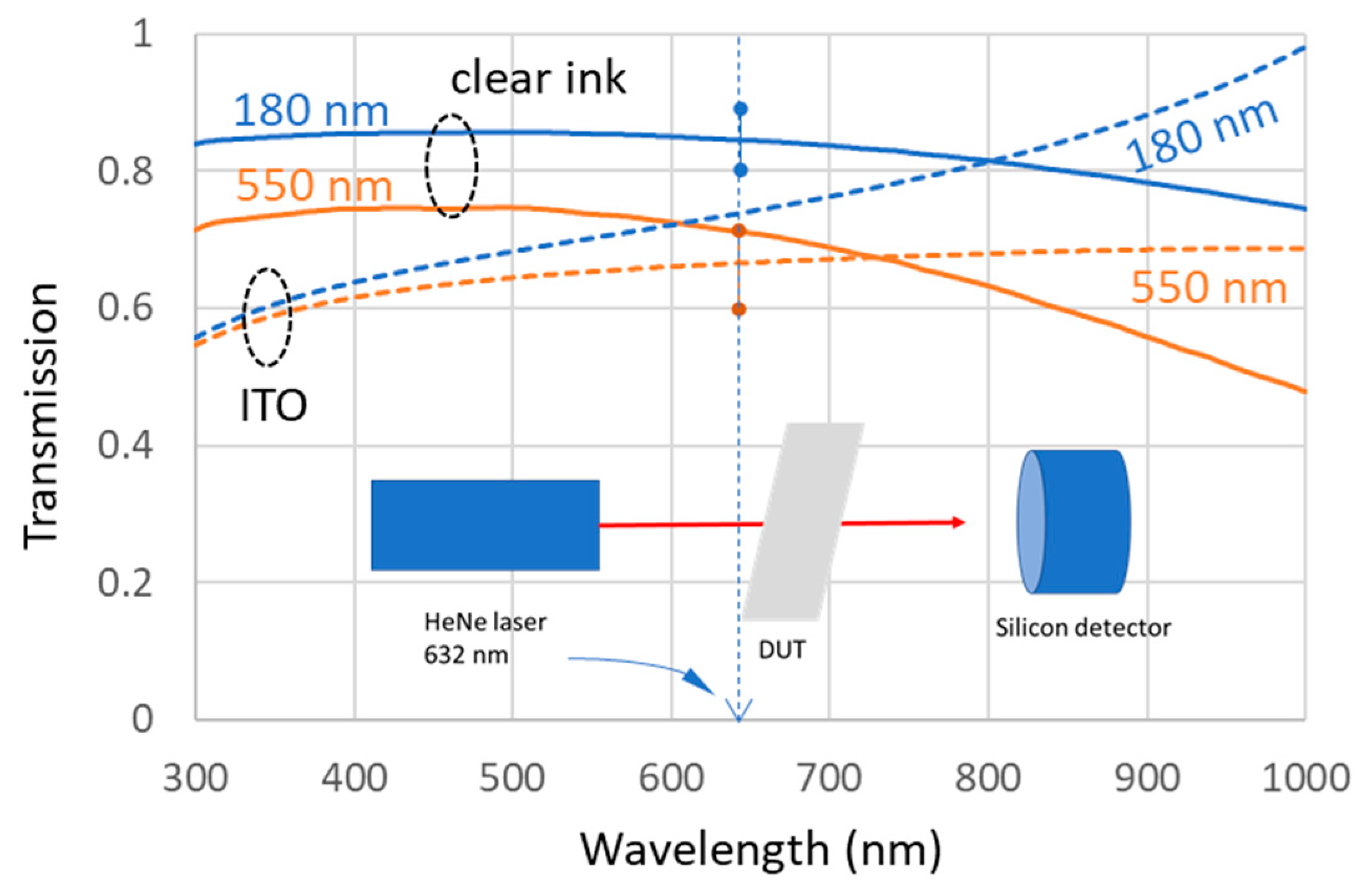
3.1. Clear Ink (CI) vs. ITO

Transparent conductive films (TCFs) are thin films that combine high optical transparency with good electrical conductivity. Indium tin oxide (ITO) is a widely used material for TCFs due to its excellent electrical and optical properties, including high transmittance in the visible range and low sheet resistance [14]. ITO films can be deposited on various substrates, including glass, plastics, and ceramics, using various techniques such as sputtering, evaporation, and chemical vapor deposition. However, the high cost and limited availability of indium have motivated the search for alternative materials for TCFs, such as graphene, carbon nanotubes, and metal nanowires [15].
Figure 4 shows typical complex refractive indices of ITO films ((a) Delta Technologies Product© Loveland, CO USA and (b) Thin Film Devices© (TFD) Anaheim, CA USA) measured using ellipsometry. The transparency of ITO films is influenced by several factors, such as the film thickness, plasma frequency, and deposition method and can be optimized for specific applications, such as LCDs or solar cells. The imaginary part k, the extinction coefficient, is related to loss and conductivity, and as shown in Figure 4 (orange line), it decreases as the wavelength decreases [16]. Therefore, the ITO film can show transparency in the visible range (400~800 nm) with a certain thickness. In case of the TFD ITO film, the extinction coefficient is lower than that of the Delta Technologies’ ITO. It could be caused by a lower concentration of oxygen vacancies in ITO controlled through annealing or doping. Clear antennas can be manufactured based on these ITOs because of both excellent optical and electric properties. However, they can be only fabricated using sputtering [14], CVD [17], sol–gel [18], or spray pyrolysis [7].
As an alternative, the CI that we used was RD Clevios™ HY Jet 2, made of AgNW/PEDOT:PSS, whose sheet resistance is in the range of 15–100 Ohm/sq (100 nm thick). This sheet resistance is comparable to that of ITO, indicating that it has similar electrical properties. To determine the transmission properties of CI film on glass, we conducted a transmission test at 632 nm using a He-Ne laser for films with thicknesses of 180 nm and 550 nm. We then adjusted the imaginary part of the complex refractive index of PEDOT:PSS as shown in Figure 5, until the calculated transmission spectra matched the experimental results. Based on the adjusted complex refractive index of PEDOT:PSS, the estimated transmission spectra as a function of wavelength are presented in Figure 6. The calculated transmissions for both samples show good agreement with the experimental results at the wavelength of the He-Ne laser (632 nm). For the 180 nm thick CI film, the transmission is greater than 70% across the entire visible spectrum, whereas for the 550 nm thick CI film, it is around 60%. The sheet resistance of the films is approximately 100 Ohm/sq, and their conductivity is about 106 S/m. The transmissions for 180 nm and 550 nm thick ITO film were also simulated to make comparisons with CI. The ITO film has a slightly lower transmission, although its electrical conductivity is comparable to that of the CI.

3.2. Characterization of Substrate

To determine the relative permittivity of glass and Delrin substrates, we employed a simple method. We fabricated microstrip lines on both substrates and measured the free spectral range (FSR) in the frequency range of interest [19,20]. The FSR was then used to calculate the relative permittivity of the substrates in the following form:
F S R = c / 2 n L
where n is the refractive index, c the speed of light, and L the length of the cavity, i.e., the length of the microstrip line. Furthermore, we used HFSS to simulate the transmission line and estimate the relative permittivity of the substrates by comparing it to the FSR. Table 4 presents the measured FSRs and the estimated relative permittivity values for two different substrate materials.

3.3. Simulation of PIFA

The performance of the PIFA was first evaluated through simulations using both HFSS and Computer-Aided Design Finite Element Method (CADFEKO). The simulations enabled the estimation of the antenna’s impedance, center frequency, bandwidth, and gain/directivity. We input the electrical properties of CI and substrates that we measured for the simulations. The antenna impedance, center frequency, and bandwidth were obtained from the S11 parameter of the antenna, which determines its frequency response and impedance [20]. The simulated antenna efficiency was calculated from the gain and directivity.
Figure 7 illustrates the radiation patterns of two PIFAs on glass and Delrin. The radiation pattern of the PIFA is dependent on its geometry and operating frequency, typically exhibiting a broad radiation pattern. The direction of maximum radiation, or beam direction, is perpendicular to the plane of the antenna. The simulated S11 of the PIFA antenna on CI/glass and CI/Delrin substrates is shown on a Smith Chart in Figure 8. It is worth noting that the reflection of the transparent antenna on the Delrin substrate exhibits less reflection, indicating that it was better impedance-matched than the glass substrate.
As shown in Figure 9, the directivity was approximately 1.9 dBi, while the gain was about −8.4 dBi. The ratio of gain to directivity represents the antenna efficiency, which was calculated to be approximately 10% or −10 dB. This low antenna efficiency was attributed to the loss of the antenna. With a conductivity of 107 S/m, the skin depth at the 2.4 GHz operating frequency was approximately 3 μm. To minimize antenna loss, the CI antenna should be thicker than 3 μm by a few times. However, due to its lower conductivity (~105 S/m) compared to copper or silver (~107 S/m), the skin depth of the CI will be larger, resulting in high loss and poor antenna efficiency. Thicker CI is necessary, but it will reduce transparency. In contrast, using DOWA ink (silver nanoparticle-based [21]) improved gain from −7 dB (glass) to 3 dB, resulting in an antenna efficiency greater than 90%. When a copper layer was assigned to the PIFA structure on the substrate in the simulation, it showed a gain of 1.7 dBi and a fractional bandwidth (FBW) of 26%. A copper PIFA on FR4 was separately fabricated and showed a realized gain of ~1.5 dBi and an FBW of 25%. Figure 10 shows the simulation of S11 to estimate bandwidths of PIFAs on CI/glass and CI/Delrin substrates, whose FBWs were 27% and 30%, respectively.
The radiation patterns of PIFAs (CI/glass and DOWA/glass) were measured as a function of angle, as shown in Figure 11. The plot provides a visual representation of how the antenna radiates electromagnetic energy in different directions. Both the polar plots displayed a wide beam width in both the top and bottom directions, aligning well with the results of the numerical simulation depicted in Figure 7. By introducing a bottom ground plane, the gain could be optimized specifically towards the top direction, resulting in a 3 dB enhancement. The measured gains exhibited significant disparities, primarily due to the considerably higher conductivity of the DOWA material, which led to minimal ohmic losses affecting the antenna’s performance.

3.4. Toward the mmWave Applications

Millimeter-wave (mmWave) frequencies have garnered significant attention in recent years for wireless communication systems due to their large bandwidth and potential for high data rates [22]. One example is WiGig, also known as 60 GHz Wi-Fi, which encompasses a set of 60 GHz wireless network protocols, including the current IEEE 802.11ad standard and the IEEE 802.11ay standard [23]. PIFAs are an attractive option for mmWave applications due to their low profile, ease of integration, and favorable radiation characteristics.
The AJ fabrication method allowed us to push the limits of antenna size. Based on the smallest gap of the CPW that the AJ printer can achieve, we found that the possible length of the arm was approximately 4 mm as shown in Figure 12, corresponding to a center frequency of approximately 60 GHz.

4. Conclusions

In this paper, we present the design and experimental characterization of an optically transparent printed PIFA antenna towards mmWave applications. The proposed antenna was fabricated using a PEDOT:PSS and silver nanowire-based AJ printing technique on glass and Delrin substrates. The antenna demonstrated a good agreement with the experimental results, showing wide FBW (25%) centered at 2.4 GHz, with a peak realized gain of −7 dBi and −3.6 dBi. The optically transparent nature of the antenna makes it suitable for integration with display systems, enabling novel applications such as transparent wireless communication systems and smart windows. The proposed antenna’s performance was compared with that of a commercially available silver nanoparticle-based PIFA, demonstrating its competitive performance in the frequency response and potential for practical implementation in mmWave communication systems. Future work may include the integration of the proposed antenna with portable and wearable wireless sensor systems to enable the development of novel transparent communication systems and the investigation of its performance in practical scenarios.

Author Contributions

Conceptualization, P.L. and D.P.; methodology, P.L., J.F. and D.P.; software, P.L. and D.P.; validation, P.L. and D.P.; formal analysis, P.L. and D.P.; investigation, P.L. and D.P.; resources, P.L. and D.P.; data curation, D.P.; writing—original draft preparation, P.L. and D.P.; writing—review and editing, P.L. and D.P.; visualization, P.L. and D.P.; supervision, E.Q. and D.P.; project administration, E.Q. All authors have read and agreed to the published version of the manuscript.

Funding

This research received no external funding.

Data Availability Statement

Data available upon request.

Acknowledgments

We thank David Elssaesser, Peter Lee, and Erica Lee for help with the experimental setup, the fabrication, and the suggestions.

Conflicts of Interest

The authors declare no conflicts of interest.

References

  1. Green Electronics Manufacturing: Creating Environmental Sensible Products. Available online: https://www.routledge.com/Green-Electronics-Manufacturing-Creating-Environmental-Sensible-Products/Wang/p/book/9781138074514 (accessed on 12 October 2023).
  2. Chishti, A.R.; Aziz, A.; Qureshi, M.A.; Abbasi, M.N.; Algarni, A.M.; Zerguine, A.; Hussain, N.; Hussain, R. Optically Transparent Antennas: A Review of the State-of-the-Art, Innovative Solutions and Future Trends. Appl. Sci. 2023, 13, 210. [Google Scholar] [CrossRef]
  3. Lee, S.Y.; Choo, M.; Jung, S.; Hong, W. Optically Transparent Nano-Patterned Antennas: A Review and Future Directions. Appl. Sci. 2018, 8, 901. [Google Scholar] [CrossRef]
  4. Wu, C.-T.; Ho, Y.-R.; Huang, D.-Z.; Huang, J.-J. AZO/Silver Nanowire Stacked Films Deposited by RF Magnetron Sputtering for Transparent Antenna. Surf. Coat. Technol. 2019, 360, 95–102. [Google Scholar] [CrossRef]
  5. Zamudio, M.E.; Behzadirad, M.; Christodoulou, C.; Busani, T. Optimization of AZO Films for Integrating Optically Transparent Antennas with Photovoltaics. Appl. Phys. Lett. 2017, 110, 234101. [Google Scholar] [CrossRef]
  6. Peter, T.; Rahman, T.A.; Cheung, S.W.; Nilavalan, R.; Abutarboush, H.F.; Vilches, A. A Novel Transparent UWB Antenna for Photovoltaic Solar Panel Integration and RF Energy Harvesting. IEEE Trans. Antennas Propag. 2014, 62, 1844–1853. [Google Scholar] [CrossRef]
  7. Sheikh, S.; Shokooh-Saremi, M.; Bagheri-Mohagheghi, M.-M. Transparent Microstrip Patch Antenna Based on Fluorine-Doped Tin Oxide Deposited by Spray Pyrolysis Technique. IET Microw. Antennas Propag. 2015, 9, 1221–1229. [Google Scholar] [CrossRef]
  8. Elmobarak Elobaid, H.A.; Abdul Rahim, S.K.; Himdi, M.; Castel, X.; Abedian Kasgari, M. A Transparent and Flexible Polymer-Fabric Tissue UWB Antenna for Future Wireless Networks. IEEE Antennas Wirel. Propag. Lett. 2017, 16, 1333–1336. [Google Scholar] [CrossRef]
  9. Malek, M.A.; Hakimi, S.; Abdul Rahim, S.K.; Evizal, A.K. Dual-Band CPW-Fed Transparent Antenna for Active RFID Tags. IEEE Antennas Wirel. Propag. Lett. 2015, 14, 919–922. [Google Scholar] [CrossRef]
  10. Chen, G.; Gu, Y.; Tsang, H.; Hines, D.R.; Das, S. The Effect of Droplet Sizes on Overspray in Aerosol-Jet Printing. Adv. Eng. Mater. 2018, 20, 1701084. [Google Scholar] [CrossRef]
  11. Hines, D.R.; Gu, Y.; Martin, A.A.; Li, P.; Fleischer, J.; Clough-Paez, A.; Stackhouse, G.; Dasgupta, A.; Das, S. Considerations of Aerosol-Jet Printing for the Fabrication of Printed Hybrid Electronic Circuits. Addit. Manuf. 2021, 47, 102325. [Google Scholar] [CrossRef]
  12. Gu, Y.; Gutierrez, D.; Das, S.; Hines, D.R. Inkwells for On-Demand Deposition Rate Measurement in Aerosol-Jet Based 3D Printing. J. Micromech. Microeng. 2017, 27, 097001. [Google Scholar] [CrossRef]
  13. Heraeus Holding Co. Available online: https://www.heraeus.com/en/hep/applications_hep/printed_electronics_hep/printed_electronics_2.html (accessed on 12 October 2023).
  14. Henry, B.M.; Erlat, A.G.; McGuigan, A.; Grovenor, C.R.M.; Briggs, G.A.D.; Tsukahara, Y.; Miyamoto, T.; Noguchi, N.; Niijima, T. Characterization of Transparent Aluminum Oxide and Indium Tin Oxide Layers on Polymer Substrates. Thin Solid Film. 2001, 382, 194–201. [Google Scholar] [CrossRef]
  15. Fortunato, E.; Ginley, D.; Hosono, H.; Paine, D.C. Transparent Conducting Oxides for Photovoltaics. MRS Bull. 2007, 32, 242–247. [Google Scholar] [CrossRef]
  16. Chen, C.-W.; Hsiao, S.-Y.; Chen, C.-Y.; Kang, H.-W.; Huang, Z.-Y.; Lin, H.-W. Optical Properties of Organometal Halide Perovskite Thin Films and General Device Structure Design Rules for Perovskite Single and Tandem Solar Cells. J. Mater. Chem. A 2015, 3, 9152–9159. [Google Scholar] [CrossRef]
  17. Wu, Z.; Ko, S.H.; Lee, D. Flexible and Stretchable Electronics; MDPI: Basel, Switzerland, 2017. [Google Scholar]
  18. Mehta, R.; Min, M.; Kaul, A.B. Sol-Gel Synthesized Indium Tin Oxide as a Transparent Conducting Oxide with Solution-Processed Black Phosphorus for Its Integration into Solar-Cells. J. Vac. Sci. Technol. B 2020, 38, 063203. [Google Scholar] [CrossRef]
  19. Yeh, P. Optical Waves in Layered Media, 2nd ed.; Wiley-Interscience: Hoboken, NJ, USA, 2005; ISBN 0-471-73192-7. [Google Scholar]
  20. Pozar, D.M. Microwave Engineering, 4th ed.; Wiley: Hoboken, NJ, USA, 2011. [Google Scholar]
  21. Dowa Electronics Materials Co., Ltd. Available online: https://www.dowa-electronics.co.jp/en/ (accessed on 12 October 2023).
  22. Chittimoju, G.; Yalavarthi, U.D. A Comprehensive Review on Millimeter Waves Applications and Antennas. J. Phys. Conf. Ser. 2021, 1804, 012205. [Google Scholar] [CrossRef]
  23. Project IEEE 802.11ay. Available online: https://www.ieee802.org/11/Reports/tgay_update.htm (accessed on 12 October 2023).
Figure 1. (left) Schematics of PIFA and (right) fabricated transparent PIFA on a glass substrate showing transparency.
Jmmp 08 00039 g001
Figure 2. Photo overview of Optomec® AJ5X system with 5-axis trunnion. Additional modifications to the tool are pointed out in the figure.
Jmmp 08 00039 g002
Figure 3. Sample traces made of clear ink. Note that both optical transparency and resistance decrease with increasing number of layers.
Jmmp 08 00039 g003
Figure 4. Complex refractive index of typical ITOs. (a) Delta Technologies Product #: CB-40IN-0111 and (b) Thin Film DevicesTM ITO. Note that the imaginary part of the refractive index decreases with a shorter wavelength. Both show a good transparency in the visible spectrum when the thickness is about a few μm.
Jmmp 08 00039 g004
Figure 5. Estimated complex refractive index of CI (PEDOT:PSS + silver nanowire). The offset of 0.01 in the imaginary part of the complex refractive index was added to get a better agreement with the experimental data.
Jmmp 08 00039 g005
Figure 6. Transmission test of CI (PEDOT:PSS + silver nanowire composite).
Jmmp 08 00039 g006
Figure 7. Gain patterns of (a) CI/glass and (b) CI/Delrin samples.
Jmmp 08 00039 g007
Figure 8. S11 on Smith Chart for CI/glass and CI/Delrin from 1.68 GHz to 3.12 GHz. The clear antenna on the Delrin substrate shows less reflection.
Jmmp 08 00039 g008
Figure 9. Simulations of directivity (D), gain (G), and efficiency (e = G/D) of (a) CI/glass and (b) CI/Delrin samples.
Jmmp 08 00039 g009
Figure 10. Reflection spectrums (left: simulation, right: experiment) of PIFAs on both glass (green) and Delrin (blue) substrates. Note that the experimental S11s of both samples show a good reflection spectrum, indicating ~1 GHz and ~0.85 GHz bandwidths for CI/glass and CI/Delrin samples, respectively.
Jmmp 08 00039 g010
Figure 11. Measured gain patterns of (top) CI/glass and (bottom) DOWA/glass. Total Max: maximum gain, Max 3 db BW: 3 dB beam width, FSPL: Free Space Path Loss. We measured the gain of the antennas by exposing it to a frequency-swept RF signal from a source horn antenna. Then, we calculated its antenna’s gain using the substitution method.
Jmmp 08 00039 g011
Figure 12. Printing multiple mmWave PIFAs on a glass substrate using AJ printing technique.
Jmmp 08 00039 g012
Table 1. Studies on transparent antenna.
TypeMethodFrequency (GHz)Performance
Patch antenna [4]Sputtering/spin-coating 2.4Narrowband
Patch antenna [5]Sputtering10Ultra-wideband
Tapered slot antenna [6]Sputtering/spin-coating 2.5Ultra-wideband
Patch antenna [7]Spray pyrolysis2.5/5Narrowband
Circular patch [8]Conductive fabric tissue2.2–25Ultra-wideband
CPW-fed patch [9]Sputtering/spin-coating 2.45/5.8Dual-band
Table 2. Important parameters for printing and fabrication.
ParametersUnitValue
Thickness of substrate (Delrin)mm1.6
Thickness of substrate (glass)mm1
Deposition rate of ink streammm3/s0.0005
Print speedmm/s3–4
Fill pitch between printed tracesμm50
Printed trace widthμm100
Thickness of circuitizationμm10
Stand-off distance (AJP)mm3–5
Table 3. Details of the antenna design and dimensions.
ParametersUnitValue
Arm length (glass)mm31
Feed location from GND (glass)mm16
Linewidth of CPW (glass)mm1.6
Gap width (glass)mm1
Thickness of substrate (glass)mm1
Arm length (Delrin)mm32.5
Feed location from GND (Delrin)mm17
Linewidth of CPW (Delrin)mm2
Gap width (Delrin)mm1
Thickness of substrate (Delrin)mm1.6
Table 4. Measured FSR, relative permittivity, center frequency, and realized antenna gain.
TypesFSR (GHz)εrfc (GHz)Gain * (dBi)
CI/glass1.24.92.45−7
CI/Delrin13.82.45−3.6
Copper/FR4-4.42.51.5
* Realized antenna gain.
Disclaimer/Publisher’s Note: The statements, opinions and data contained in all publications are solely those of the individual author(s) and contributor(s) and not of MDPI and/or the editor(s). MDPI and/or the editor(s) disclaim responsibility for any injury to people or property resulting from any ideas, methods, instructions or products referred to in the content.

