Article

Freeform Hybrid Manufacturing: Binderjet, Structured Light Scanning, Confocal Microscopy, and CNC Machining †

1
Department of Mechanical, Aerospace, and Biomedical Engineering, University of Tennessee, Knoxville, TN 37996, USA
2
Manufacturing Science Division, Oak Ridge National Laboratory, Oak Ridge, TN 37830, USA
*
Author to whom correspondence should be addressed.
This paper is an extended version of our paper published in Dvorak, J.; Gilmer, D.; Zameroski, R.; Cornelius, A.; Schmitz, T. Fabrication of freeform silicon carbide components by hybrid manufacturing. In Proceedings of the American Society for Precision Engineering Annual Meeting, Minneapolis, MN, USA, 1–5 November 2022.
J. Manuf. Mater. Process. 2023, 7(2), 79; https://doi.org/10.3390/jmmp7020079
Submission received: 17 March 2023 / Revised: 11 April 2023 / Accepted: 13 April 2023 / Published: 18 April 2023
(This article belongs to the Special Issue Hybrid Manufacturing)

Abstract

:
This paper describes a hybrid manufacturing approach for silicon carbide (SiC) freeform surfaces using binder jet additive manufacturing (BJAM) to print the preform and machining to obtain the design geometry. Although additive manufacturing (AM) techniques such as BJAM allow for the fabrication of complex geometries, additional machining or grinding is often required to achieve the desired surface finish and shape. Hybrid manufacturing has been shown to provide an effective solution. However, hybrid manufacturing also has its own challenges, depending on the combination of processes. For example, when the subtractive and additive manufacturing steps are performed sequentially on separate systems, it is necessary to define a common coordinate system for part transfer. This can be difficult because AM preforms do not inherently contain features that can serve as datums. Additionally, it is important to confirm that the intended final geometry is contained within the AM preform. The approach described here addresses these challenges by using structured light scanning to create a stock model for machining. Results show that a freeform surface was machined with approximately 70 µm of maximum deviation from that which was planned.

1. Introduction

Freeform optics are widely considered a disruptive technology in the optics industry [1,2,3,4]. Kumar et al. state that freeform optics differ from traditional optics and provide the following benefits [3]:
  • Enhancement of optical performance or the same optical performance as a compact system is maintained, such as an expanded field of view and aberration-free surfaces.
  • Quantitative reduction in optical components of systems, reducing the overall cost.
  • Simplified assembly because of a few optical components. For example, freeform surfaces fabricated on a single monolith.
  • Miniaturization of optical systems.
  • Reduction in the weight of the optical system and a more compact size.
  • Improvements in the capabilities of optical designers and innovation in optics.
Freeform optics do not follow the radial symmetry imposed for traditional optical system designs. This complex geometry can result in difficulties with alignments, manufacturing, and inspection [1,2,3,5,6]. Additionally, optics generally require tighter tolerances and surface finishes than traditional manufacturing processes can achieve. Ultra-precision grinding, polishing, or diamond turning are typically used to meet these requirements [2]. Ceramics such as silicon carbide (SiC) have recently been implemented for optical applications with the added benefit of superior material properties over metals [7]. SiC has excellent physical, thermal, and mechanical properties, making it attractive for engineering applications such as heat exchangers, high-temperature seals and valves, armor, mirrors and optics, and electronics. Furthermore, much work is being done in the additive manufacturing of SiC as AM offers increased design freedom over traditional manufacturing methods. BJAM of SiC provides higher feature resolution and volume throughput than other AM methods. BJAM of SiC has positive implications for nuclear applications, embedded sensors, and material savings, for example [8,9]. Horvath et al. discuss the benefits of BJAM for SiC and show results for grinding the printed SiC to produce optical components [7]. The work presented here describes the fabrication of a freeform surface on a BJAM SiC sample using ball end milling as a precursor to finish polishing or grinding. These efforts establish the basis for the hybrid manufacturing of BJAM SiC freeform optics.
BJAM is a process in which powder is selectively bound together by depositing a binder into a metal, ceramic, or polymeric powder bed using an inkjet printhead. The layer by layer deposition is used to form a three-dimensional part [10,11]. In each layer of printing, a new layer of powder is spread within the build box, and more binder is selectively deposited. The process is repeated until the desired three-dimensional geometry is created [12]. Print parameters may cause errors in the geometry of the printed part (or preform), especially when working at large scale [13]. In most iterations of the BJAM process, the build box is removed from the machine after printing is completed and placed into a low-temperature oven where the polymer used to bind the particle together is solidified. After this curing step, the build box is then removed from the oven, and the “green” or polymer-bound powder part is depowdered/removed from the surrounding powder. The green preform is brittle and fragile [14,15]. The part must then complete further densification during post processing to achieve higher density and enable handling [14,15,16,17]. In this work, cyanoacrylate is used for the temporary densification and handling of BJAM SiC. The cyanoacrylate is then eliminated during heating in a furnace. Traditional sample densification can also be included in this step [18].
This work explores the implementation of hybrid manufacturing for BJAM SiC samples and builds on initial work reported by Dvorak et al. [19]. Related works that collectively discuss this scenario are summarized in the following paragraphs.
Webster et al. defined hybrid manufacturing as follows:
In-situ or series combination of an additive manufacturing process and secondary energy sources in which physical mechanisms are fundamentally altered/controlled to affect the resulting properties of the material and/or part [20].
Hybrid manufacturing provides reduced energy and material use for certain material removal ratios [21]. Zhu et al. completed a review of hybrid manufacturing processes and discussed a need for integration between processes, further process-planning methods, modeling of hybrid capabilities, and additional standards [22]. Chu et al. reviewed hybrid manufacturing at the micro/nano scale and found that machining was the most common hybrid manufacturing process for the 57 processes covered [23]. Cornelius et al. completed hybrid manufacturing of an additive friction stir deposition preform using tooling spheres and structured light scanning for stock model generation and coordinate system definition and its transfer to the follow-on machining step [24]. A similar methodology is used in this work.
Cornelius et al. demonstrated the hybrid manufacturing method for the five-axis computer numerical control (CNC) machining of a wire arc additive manufacturing (WAAM) component [25]. Dvorak et al. used the same hybrid manufacturing method for the three-axis machining of a WAAM preform with a focus on how the methodology provides essential components of a machining digital twin for hybrid manufacturing [26]. Mali et al. completed a comprehensive review of freeform surface milling [27]. They found that for the 168 papers considered, only 11% explored “other materials” as opposed to aluminum and steel alloys. They discuss path planning and force prediction for the ball end milling of freeform surfaces. Ball end milling is used in this work. Masood et al. described the use of point cloud data for complex surface tool path generation [28]. They developed an algorithm for the direct machining of a scanned component in order to eliminate steps in the computer-aided design (CAD) conversion of a reverse engineering scan.
Fiducials and structured light scanning are key components of the hybrid manufacturing sequence proposed in this work. Fiducials are often used in manufacturing for machine calibration or part location [5,29]. Brunelle et al. discussed the importance of fiducials for freeform optics and stated the following:
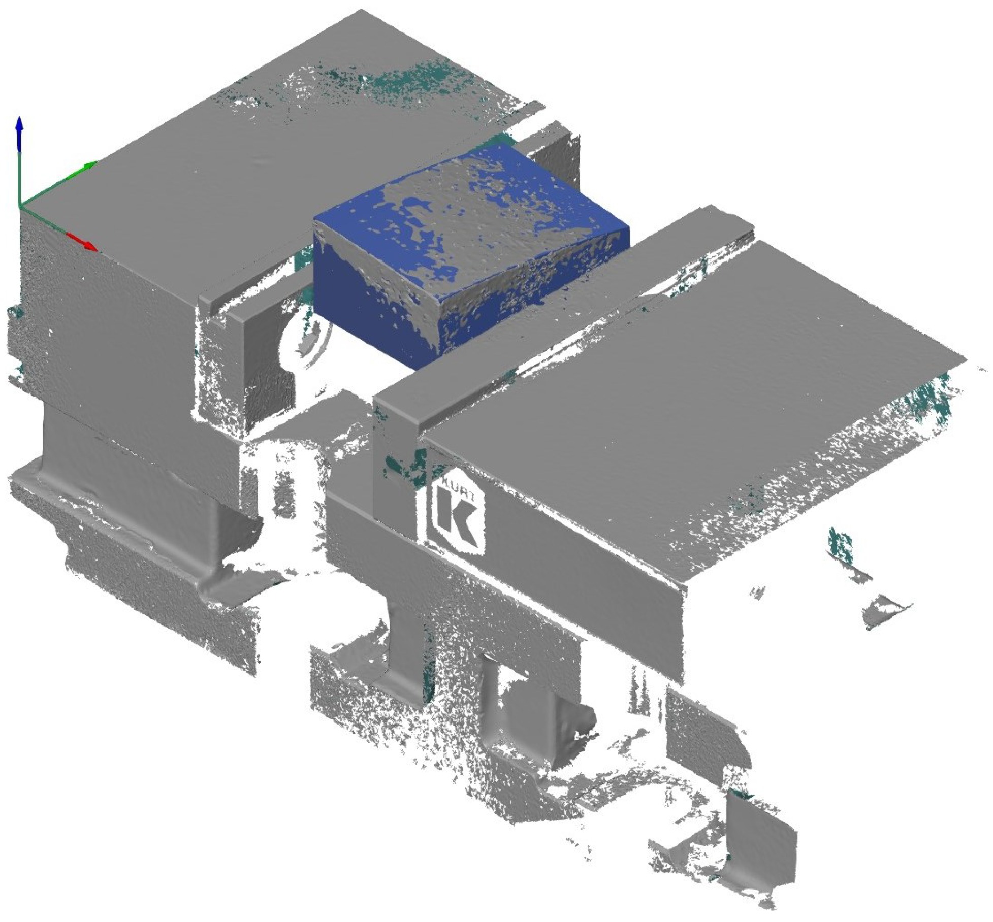
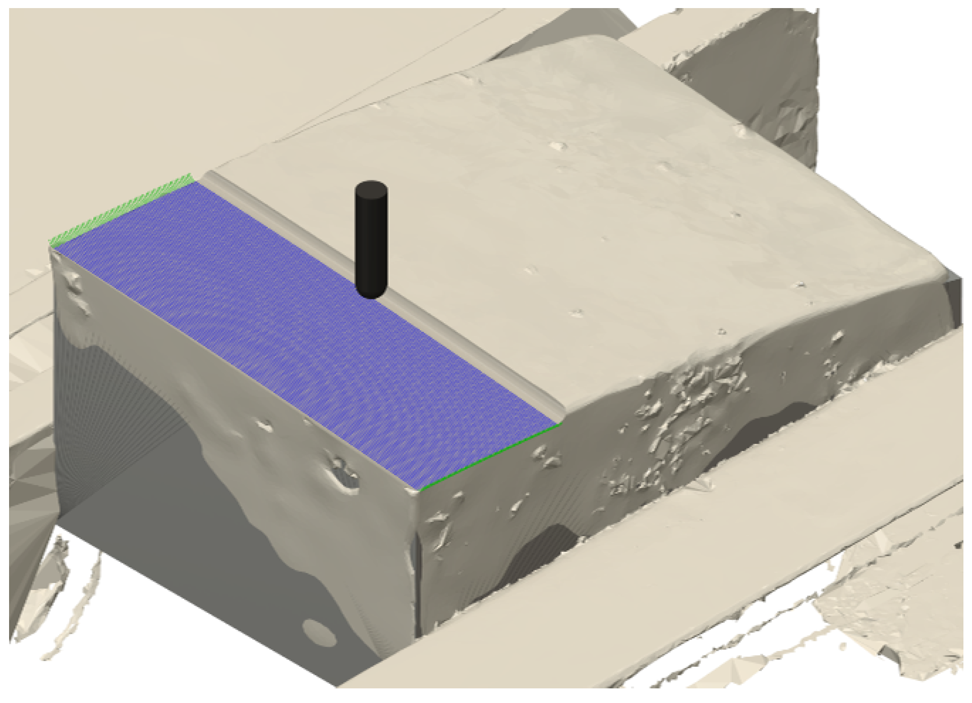
Alignment fiducials (also) enable more precise locating of the surface during the manufacturing process.
Furthermore, the authors stated that fiducials can serve as alignment features for metrology equipment such as a coordinate measuring machine (CMM) [5]. Fiducials are used to locate the surface for machining in this work. Cornelius et al. used precision tooling spheres for hybrid manufacturing coordinate system (CS) definition and transfer [24]. This work applies the same methodology but uses ground surfaces of the vise that clamps the SiC preform rather than tooling spheres. Wang et al. defined an uncertainty analysis model of a fiducial-aided calibration and positioning system for the precision manufacturing of freeform optics [6]. They showed that the transformation uncertainty is small and that fiducial-aided calibration and positioning is most sensitive to the measurements from the on-machine measurement system. Srinivasan et al. demonstrated the use of structured light scanning to automatically transfer a CS defined by pre-machined features from a CNC machine [30]. Woody et al. showed that a fiducial calibration system can be used to transfer accuracy of a CMM to a machine tool [31]. They presented an uncertainty analysis to aid in the selection of fiducials, measurement devices, and a machine tool for the desired part accuracy.
Structured light scanning is a widely-used approach for measurements in manufacturing environments [32]. Prior research has explored its accuracy. Mendricky developed an acceptance test based on several error metrics and the VDI/VDE standard 2643—part 3 to evaluate the accuracy of optical systems [33]. Boehm et al. evaluated the accuracy of commercial sensors based on similar error metrics [34]. Dickin et al. attempted to map and correct the distortion of structured light scanners [35]. They developed a methodology for assessing scanner uncertainty and used results to compute correction mappings and reduce residual error. Eiriksson et al. showed that the system calibration parameters influence measurement results [36]. They found that a custom setup with off-the-shelf, low-cost components can provide comparable and, in some cases, better results than a commercial system.
Li et al. implemented structured light for the automatic path planning of grinding operations using an industrial manipulator [37]. Palousek et al. discussed the effects of reflectance and the use of titanium or chalk spray to coat part surfaces on measurement results [38]. They evaluated the type A measurement uncertainty using titanium or chalk spray. In this work, titanium spray was applied to the ground surfaces on the vise (to reduce reflectivity) but not on the BJAM SiC preform.
The aim of this work is to manufacture an SiC freeform surface using a hybrid manufacturing sequence that employs BJAM to produce the preform, structured light scanning for the coordinate system and stock model definition, and the ball end milling of the SiC surface for improved dimensions and finish. The application domain for this work is SiC optics that require freeform surfaces and low surface roughness values. Additionally, this study evaluates the viability of machining cyanoacrylate-infiltrated BJAM SiC preforms. The intent is to improve the manufacturability of SiC optics and reduce material use.

2. Materials and Methods

An SiC preform with a toroidal freeform surface was fabricated using BJAM and then infiltrated with cyanoacrylate. This enabled the handling and machining of the preform. A novel method for defining the coordinate system of the SiC preform using structured light scanning was used. This involved clamping the preform in a vise and selecting specific features on the vise to define the local coordinate system. This coordinate system was then located in the milling machine using the on-machine probe and probing routines. This method overcomes inherent hybrid manufacturing challenges by accurately aligning the digital design with the AM preform scan model. The structured light scan and coordinate system also enable toolpath generation and simulation. These steps and components are next described in detail.
A surface was modeled using a toroidal freeform:
Z = C x X 2 + C y Y 2 1 + 1 C x 2 X 2 C y 2 Y 2 ,
where C x and C y are constants [39]. Values used were based on maximum available print and measurement volumes and are tabulated in Table 1. The modeled surface is shown in Figure 1.
To enable printing and fixturing, a 12.7 mm tall base from the surface’s lowest point was added as shown in Figure 2. The CAD surface model was generated in standard tessellation language (STL) format using MATLAB, and the 12.7 mm base was added using OpenSCAD.
This geometry was printed using an Innovent binder jet printer from ExOne Company, North Huntingdon, PA, USA. ExOne Company provided their aqueous binder AquaFuse for the printing process. The printer was equipped with a printhead containing four SL-128 AA inkjet modules from Fujifilm, Minato City, Tokyo, Japan. This configuration creates 40 pL droplets and has 128 nozzles with a 50 µm diameter nozzle size.
A heater was used during the printing process to evaporate small amounts of solvent from the printing fluid. This was done to increase the viscosity of the fluid and prevent the binder solution from flowing outside of the area in which it was deposited, which is known to adversely affect geometric accuracy. In the software, the user defines a target bed temperature, and the machine auto-adjusts the heater output power (0–100%) to reach and maintain the target temperature. Initially, the heater power is between 70% and 90% and reduces to around 30% once the temperature is reached. Layer thickness measures the thickness of the powder layer that is spread onto the build platform. Depending on particle size (recommended around twice the thickness of the mean particle diameter), part definition and print time can be adjusted. The layer thickness was 100 µm and the droplet volume was 37.4 pL in this study. The heat and saturation were altered for each specimen to achieve uniform printing. Print parameters are provided in Table 2. The printed preform is shown in the left panel of Figure 3.
The sample was infiltrated with approximately 75 mL of thin 5 cP cyanoacrylate to enable handling and reduce fragility; see right panel of Figure 3. Cyanoacrylate was poured over the top surface until it was observed to exit the bottom of the preform. The preform was then placed on a polypropylene sheet to prevent bonding to this sheet as it dried. Exhausted cyanoacrylate was lightly brushed off after 24 h of curing and immediately set up for machining. The sample was clamped in a 101.6 mm wide vise; see Figure 4. A structured light scan of the preform was completed using a GOM ATOS Core 200 (ZEISS, Oberkochen, Baden-Württemberg, Germany) to establish the work coordinate system (WCS) and enable stock model generation after applying 1.5 mm scanner targets directly onto the vise. Prior to scanning, AESUB (Recklinghausen, Nordrhein-Westfalen, Germany) Blue scanning spray was applied only to the vise surfaces to reduce reflectivity and improve scan quality. GOM Inspect (ZEISS, Oberkochen, Baden-Württemberg, Germany) was used to perform a best fit of the CAD to the scan as shown in Figure 5. A maximum search distance of 0.2 mm resulted in an average deviation of 63 µm. The WCS was defined by fitting three planes to three ground surfaces of the vise using a Gaussian best fit and 99.7% of the points from the scanned point cloud. The adjustment results for these three fitting planes showed a standard deviation of {19.9, 11.3, and 7.3} µm.
A 2.381 mm diameter, two flute ball end mill (YG1 model 99573) was selected for machining. The diamond coating was appropriate for machining abrasive materials such as SiC. The CAD model was shifted down 1 mm in the Z direction to set the depth of cut. A Haas OM2 (Haas Automation, Inc., Oxnard, CA, USA) three-axis CNC machining center was used for preform machining. Feeds and speeds were selected using the maximum recommended surface speed for the ball end mill and the maximum spindle speed for the OM2, as well as the desired surface finish. This resulted in a spindle speed of 30,000 rpm (225 m/min surface speed) and feed per tooth of 0.015 mm (881 mm/min feed rate). A simulation of the milling process with a target average roughness of 1 µm provided a stepover of 0.193 mm [40]. These parameters resulted in a 15-min cutting time. The tool’s dynamic response was measured by tap testing in the machine X and Y directions to ensure these parameters would result in a stable cut [40,41]. It was found that the limiting cutting depth was larger than the desired 1 mm by a significant amount, so machining stability was not a limitation for this work. This is a primary motivation for machining prior to traditional BJAM SiC densification.
The CAD and scan were both exported with the WCS as the origin and imported into Fusion 360 (Autodesk, San Rafael, CA, USA) for computer aided manufacturing (CAM) and tool path programming. The WCS was used to define the model origin and orientation. A parallel finishing operation was selected that maintained parallel passes in the XY plane and followed the surface in the Z direction. The scan enabled a full simulation of the programmed tool paths; see Figure 6. The vise with the preform still clamped was bolted to the Haas OM2 machine table and manually aligned to the machine X and Y axes using a dial indicator. The ground faces of the vise selected for the WCS were probed using a Haimer 3D (Haimer, Hollenbach, Germany) sensor that was previously calibrated to be zero at the spindle centerline. Figure 7 displays the Z surface probing. The Z zero was set to be the difference between the machine table and the probed surface. Tool offsets were set relative to the machine table. The X and Y zeros were set by probing their respective faces with the Haimer 3D sensor. The program was then executed, and the preform was machined. The machined SiC sample is shown in Figure 8.

3. Results

The geometry and surface finish of the machined preform were measured to compare with the commanded values. The SiC sample, still clamped in the vise, was again scanned using the GOM Core 200 structured light scanner. This enabled the WCS to again be defined by the same method. The CAD was aligned in the same orientation (i.e., prior to machining) in the post-machining scan. A surface error map between the scan and CAD is shown in Figure 9. It is observed that the surface was overcut by approximately 10–70 µm relative to the commanded surface with the majority of the surface in the 50 µm range (dark green).
An Alicona InfiniteFocusSL 3D measurement system was used to scan the surface of the SiC sample before and after machining. An ABS sample printed using fused filament fabrication (FFF), but which otherwise used the same manufacturing steps, was also measured for comparison. This was completed to determine differences in surface finish and to review trends in the final surfaces. Three-dimensional scans of the final surface for both samples were exported as point clouds and imported into GOM Inspect. The commanded 3D surface was then best fit to these point clouds. Note that these results do not retain the original pre-machining alignment because the WCS was not transferred to the 3D measurement system. Results for the SiC sample are shown in Figure 10, and the ABS sample results are provided in Figure 11. The range of the ABS sample was approximately 40 µm while the SiC sample was approximately 140 µm, indicating that there is a fundamental difference associated with either the SiC material or the machining process.
The surface finish of the SiC part was next analyzed before and after machining. Five traces were completed that conformed to ISO 4287 and 4288. A cutoff wavelength of 8 mm was used for the pre-machining measurement, and 2.5 mm was used for the post-machining measurement. The results are provided in Table 3. Note that the BJAM SiC particles ranged from 30 µm to 40 µm in size. These results show that the surface finish of the finished SiC component was almost 10 times higher on average than the theoretical value of 1 µm, whereas the ABS sample was only 2 to 2.7 times higher. This indicates a need for further post-processing of the SiC sample, smaller stepover, or smaller SiC particle size.
The Alicona software was used to create a surface roughness image for both machined samples using a fifth-degree polynomial fitting function to remove form; see Figure 12 and Figure 13. It is observed that machining marks are visible in the ABS sample, as well as gaps in the infill pattern, but layer lines are not observed. The opposite is the case for the SiC sample, where layer lines are still clearly observed and no machining marks are visible. This further indicates a failure to properly machine away layer lines from the SiC sample.

4. Discussion

This work presented a novel hybrid manufacturing approach for BJAM preforms using structured light scanning to generate a stock model for the machining of the freeform surface. The freeform surface was modeled with a toroid to enable direct comparison to the machined surface. A vise was used to clamp the preform, and both the vise and preform were scanned. This enabled the WCS to be defined using ground surfaces on the vise so that no datum surfaces were required on the part to provide coordinate system transfer between AM and machining. Measurements were completed after machining to compare the machined surface and form to the required geometry. The measurement strategy included the same coordinate system to enable direct comparison to the prescribed surface equation. Both the BJAM SiC sample and FFF ABS samples were prepared to assess the sensitivity to the preform material. Error are discussed for different measurands and measurement systems across both samples.
Several contributors to error in the machined surface were identified. These included the accuracy of the GOM ATOS Core 200 structured light scanner, the accuracy of the Haas OM2 three-axis milling machine, and the unique physical nature of the BJAM SiC preform. Zeiss states that the ATOS Core 200 uncertainty is 80 µm for its work volume. It was found that the fitting of planes to the surfaces of the vise for WCS definition had a standard deviation ranging from 7 µm to 20 µm. Any deviation in fitted planes prior to machining would result in error from what would be physically probed on the vise. Additionally, error in the fitted planes after machining would alter surface error results. The accuracy of the Haas OM2 milling machine was of concern as it is not a typical ultra-precision system for optical or freeform applications. The nature of the SiC sample was also considered. As noted, the SiC particles were approximately 30 µm to 40 µm in size. Finally, the effect of cyanoacrylate infiltration on part geometry was not well understood. Due to these issues, an ABS sample was fabricated using FFF for comparison. This enabled the same geometry to be evaluated but without the BJAM considerations.
The machined SiC and ABS parts were measured using the structured light scanner with the preform still in the vise. This enabled the machined surface to be compared to the commanded surface in the same alignment defined for machining. This result showed that error in the SiC sample was approximately −70 µm to 70 µm and the ABS sample error ranged from approximately 10 µm to −30 µm. Note that negative values indicate that the part was overcut relative to the intended surface. The difference in form observed in Figure 10 and Figure 11 is proposed to be a product of the cyanoacrylate infiltration. It is believed that the infiltration caused the sample to expand after machining due to insufficient cure time prior to machining (24 h). Specifically, it is believed that the circular “bulging” nature of the SiC preform is due to this insufficient cure time between densification and clamping/machining of the preform. Given a longer cure time to reach final dimensions, the machining step would ideally provide final geometry for post-machining steps. The difference in results for the surface error of the SiC and ABS sample provides some justification for this argument. Note that for the SiC sample, 24 h passed between infiltration and clamping/machining, immediately followed by scanning with the GOM system. Alicona scans were taken a week later after removing the machined part from the vise.
In addition to form, the surface finish was also evaluated. An Alicona 3D optical measurement system was used to quantify the surface finish and detailed trends observed in the finished surfaces. The selected tool geometry and machining parameters provided a theoretical average roughness of 1 µm. The average roughness of the SiC sample ranged from 8.9 µm to 9.7 µm, while the ABS sample average roughness ranged from 2.0 µm to 2.7 µm. As with most machining processes, achieving the theoretical surface finish was not expected. However, this difference between the SiC and ABS samples proves there are limitations imposed by the nature of the SiC preform. By performing a best fit of the commanded freeform surface to the 3D optical measurement results, surface finish trends could be identified. It was observed that the SiC component surface extends radially from the center, while the ABS component is more linear from the sides. Layer lines of the BJAM SiC sample are observed post-machining, further indicating a failure to properly machine the surface.
This work provided an initial investigation into the hybrid manufacturing of freeform BJAM SiC samples for optical applications. The preform was machined with a temporary cyanoacrylate infiltration as opposed to the post densification machining of the SiC component. Machining the infiltrated, rather than densified, preform meant that the part had a lower hardness during material removal. It is well known that harder materials produce higher machining forces and reduce surface quality. Mali et al. state that machining forces have the largest impact on freeform surface quality [27]. Future work will explore densifying the machined sample to quantify geometry and surface finish in the post densification state and determine the viability of machining prior to SiC densification.
Future work is planned. The topics to be investigated are (1) the uncertainty evaluation for structured light scanning and optical 3D surface measurement and (2) repeatability analysis for the geometry and surface finish of hybrid manufactured freeform BJAM SiC sample parts.

5. Conclusions

Based on the presented work and results, the following conclusions are made:
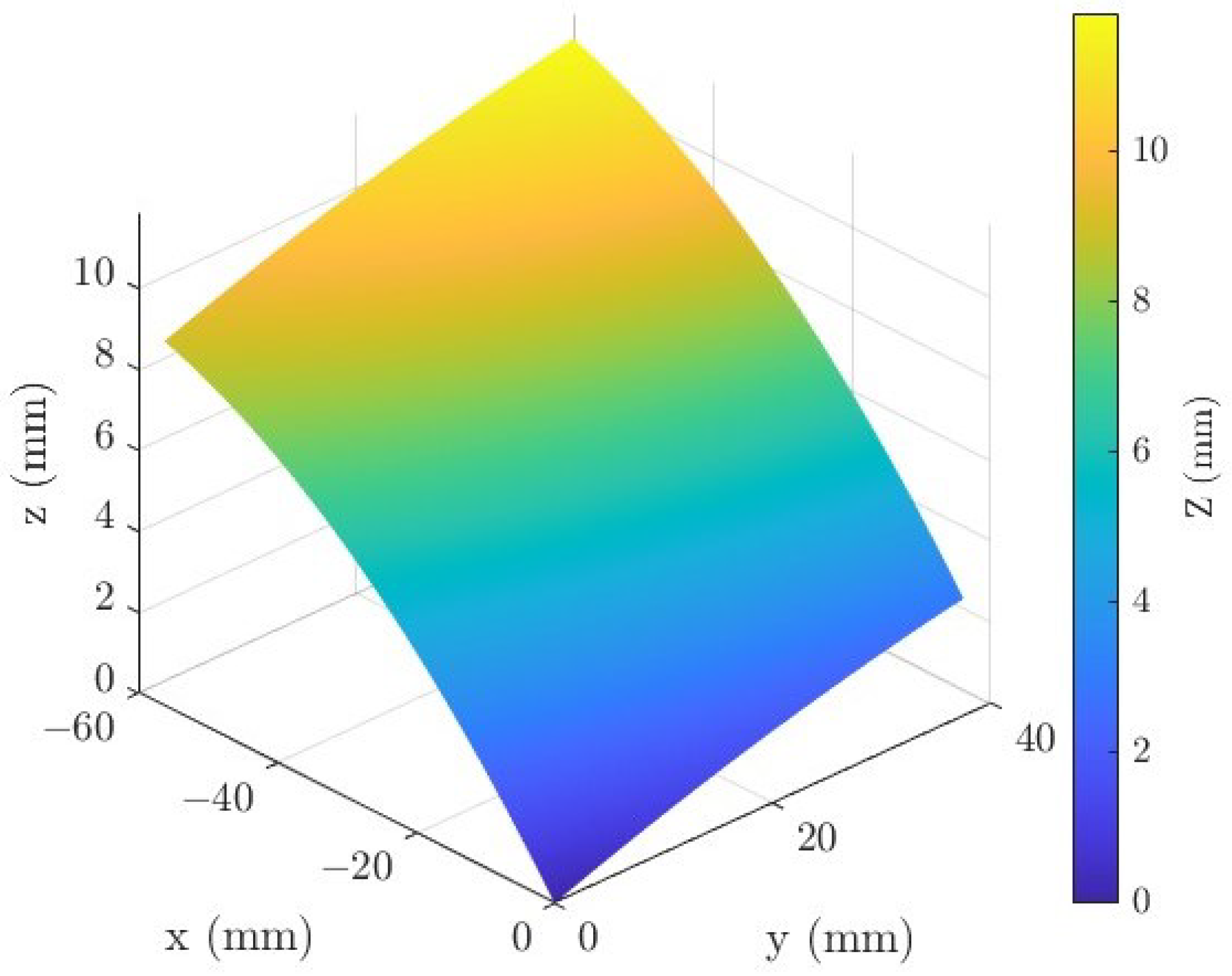
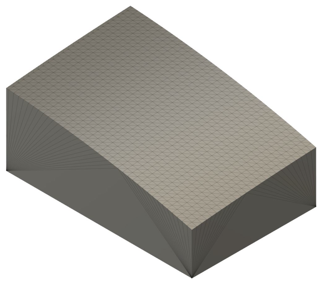
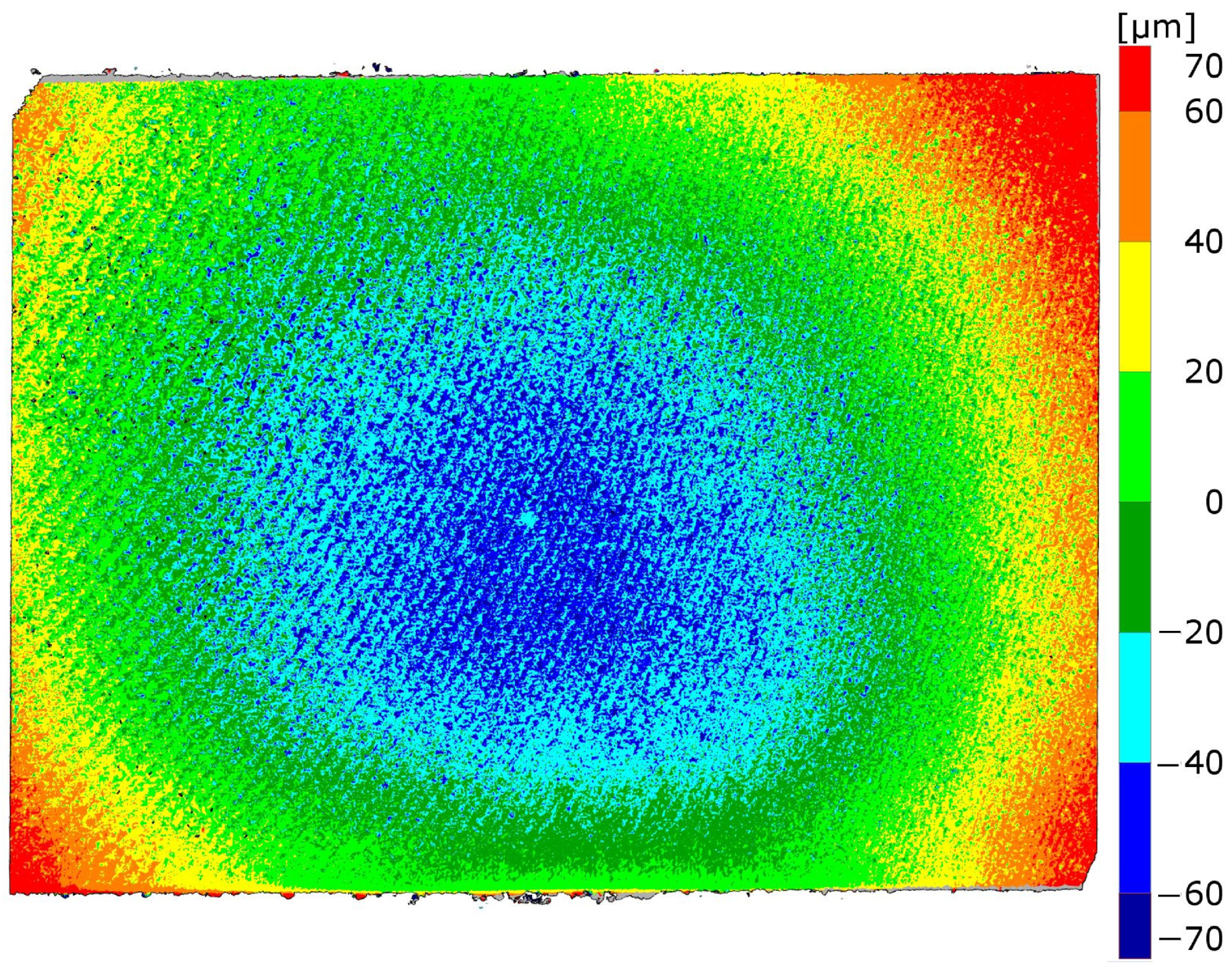
  • Hybrid manufacturing of freeform surfaces on BJAM SiC samples using structured light scanning for stock model generation and WCS definition and traditional three-axis milling is possible, although final part accuracy requires additional study.
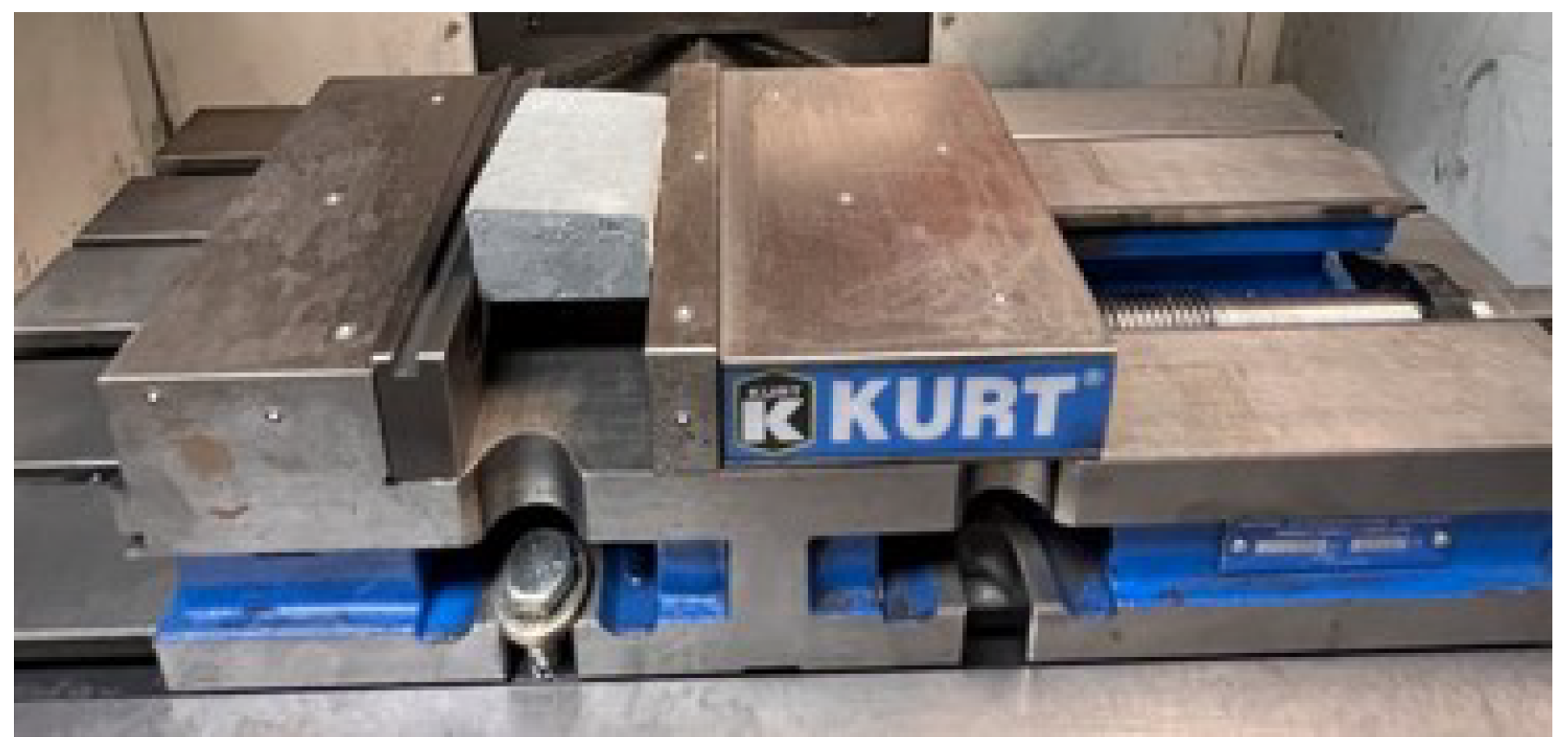
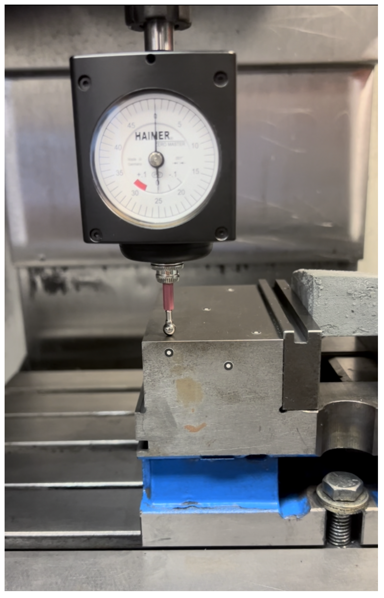
  • The workpiece clamping system (a vise in this case) can provide fiducials for WCS definition and alignment in a machine tool. The strategy includes both the clamping system and part in the structured light scan to enable the coordinate system to be established independently of the part design.
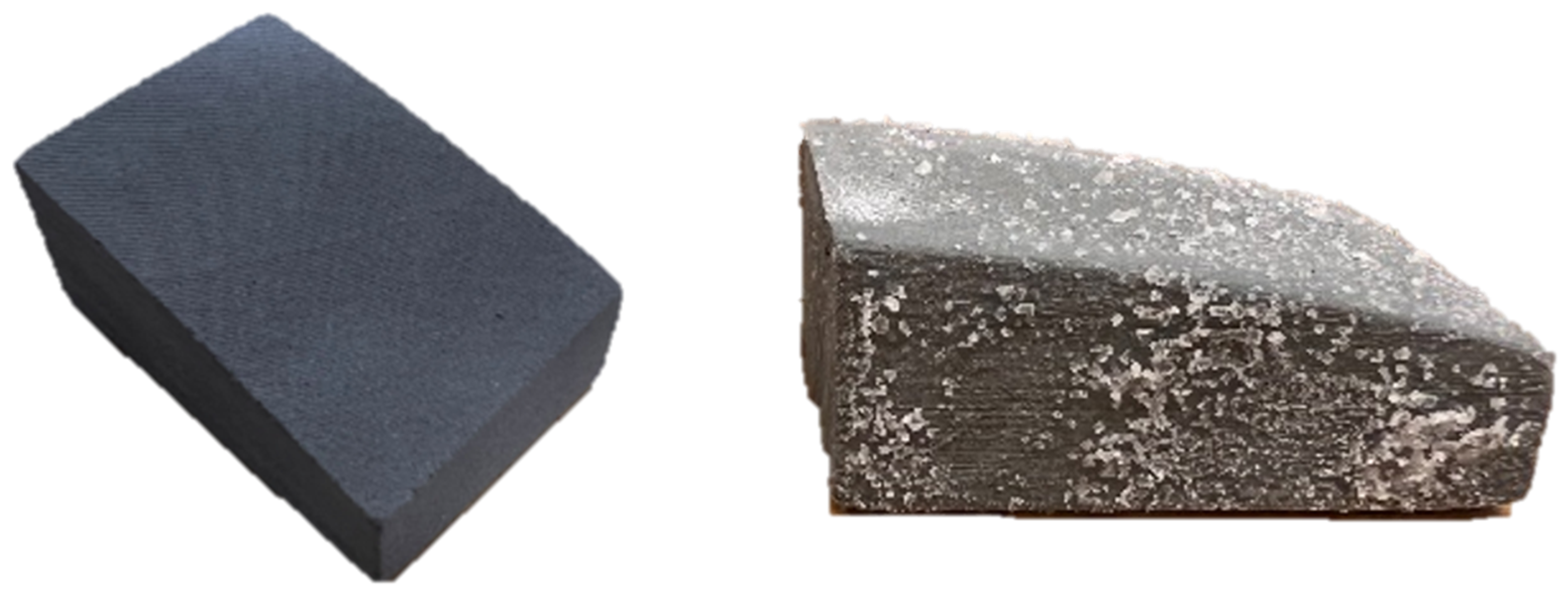
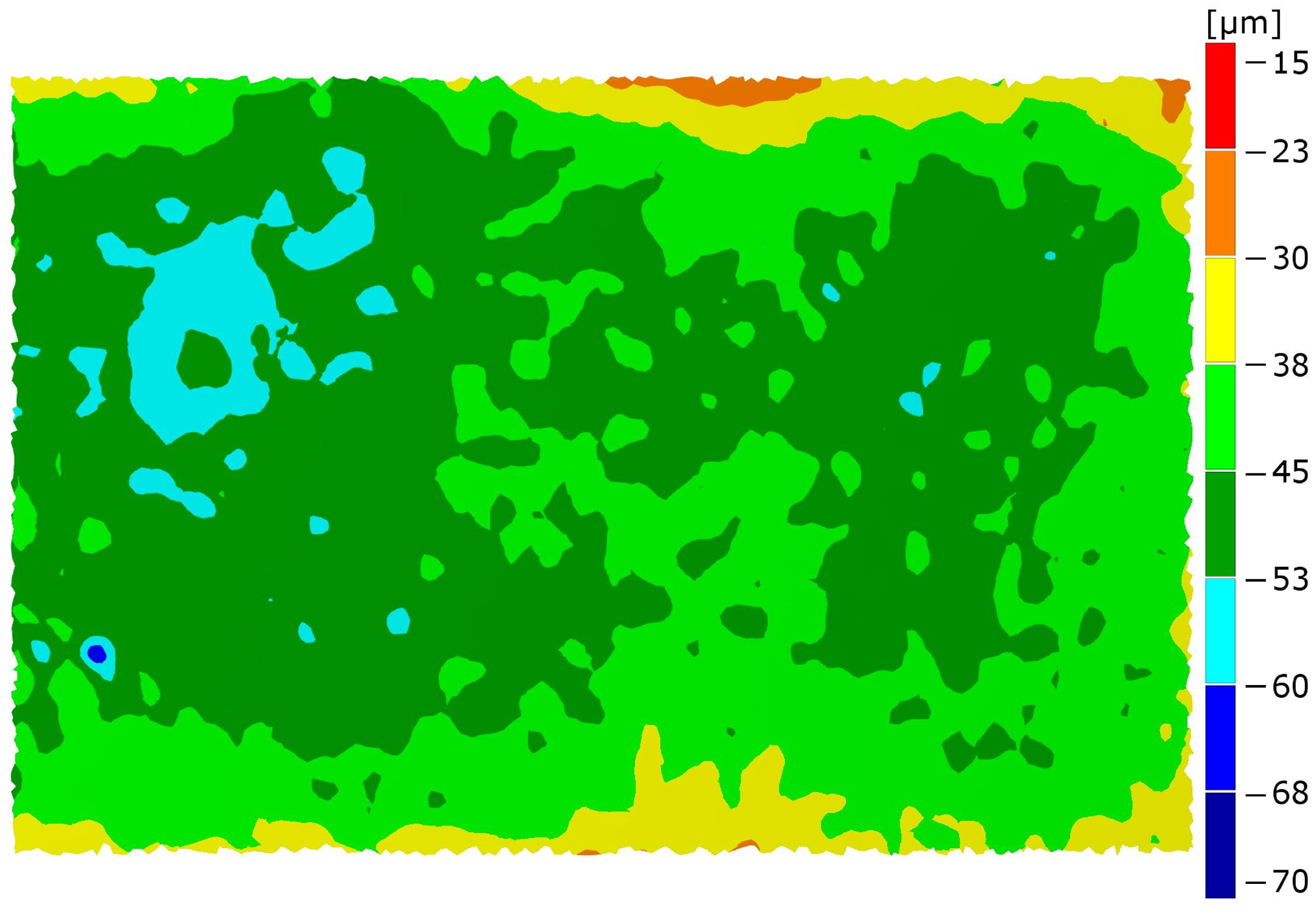
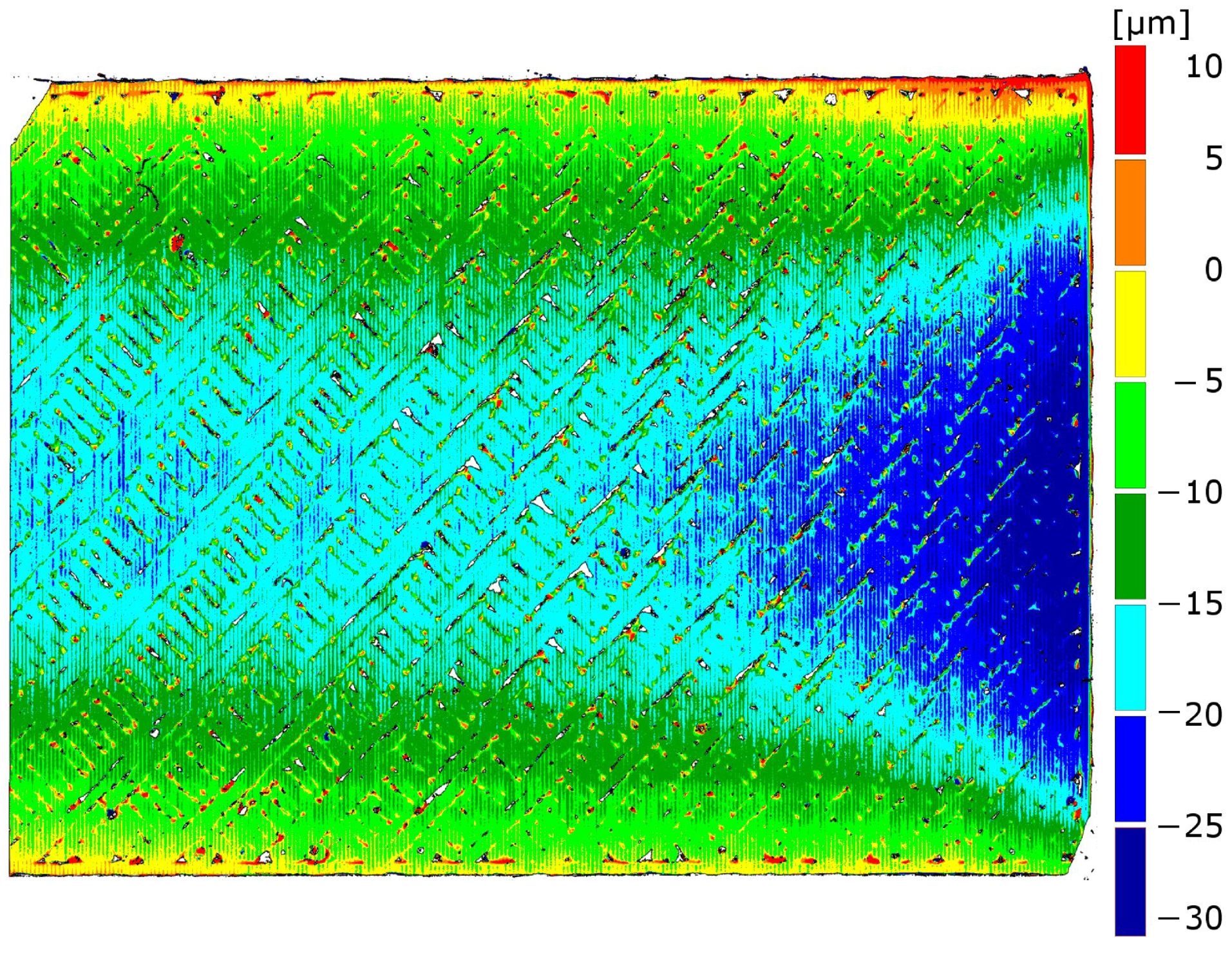
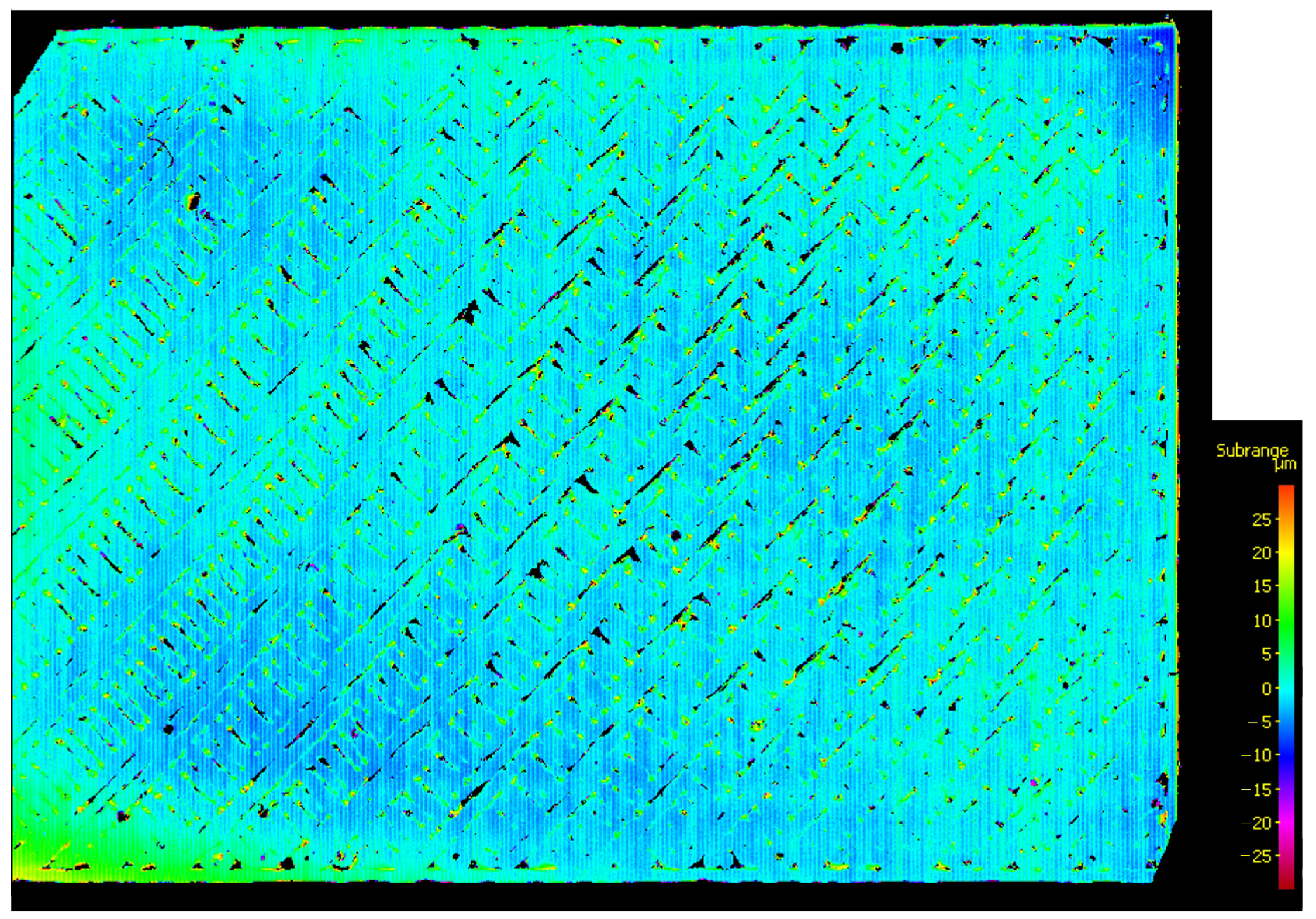
  • The ball end milling of a BJAM SiC sample infiltrated with cyanoacrylate was not able to properly remove layer lines from the surface resulting in poor surface finish.
  • The surface finish of the machined BJAM SiC sample was worse than a FFF ABS sample machined using the same parameters and tool paths. Smaller particles or further post-processing may be required for hybrid manufacturing of SiC samples depending on the application.
  • Infiltration of BJAM SiC samples can impact machining results. In this work, it is proposed that cyanoacrylate curing time can affect the final geometry of the preform.

Author Contributions

Conceptualization, J.D. and T.S.; methodology, J.D., D.G., A.C. and T.S.; software, J.D. and R.Z.; validation, J.D., T.S. and A.C.; formal analysis, J.D.; investigation, J.D.; resources, D.G. and T.S.; data curation, J.D.; writing—original draft preparation, J.D.; writing—review and editing, J.D., D.G., A.C. and T.S.; visualization, J.D.; supervision, T.S.; project administration, T.S.; funding acquisition, T.S. All authors have read and agreed to the published version of the manuscript.

Funding

This research was funded by the Department of Energy grant number DE-AC05-00OR22725.

Institutional Review Board Statement

Not applicable.

Informed Consent Statement

Not applicable.

Data Availability Statement

Data is available within article or upon request.

Acknowledgments

This manuscript has been authored by UT-Battelle, LLC, under contract DE-AC05-00OR22725 with the US Department of Energy (DOE). The US government retains, and the publisher, by accepting the article for publication, acknowledges that the US government retains, a nonexclusive, paid-up, irrevocable, worldwide license to publish or reproduce the published form of this manuscript, or allow others to do so, for US government purposes. DOE will provide public access to these results of federally sponsored research in accordance with the DOE Public Access Plan (http://energy.gov/downloads/doe-public-access-plan, accessed on 16 February 2023).

Conflicts of Interest

The authors declare no conflict of interest.

Abbreviations

The following abbreviations are used in this manuscript:
SiCSilicon carbide
BJAMBinder jet additive manufacturing
AMAdditive manufacturing
CNCComputer numerical control
WAAMWire arc additive manufacturing
CADComputer-aided design
CSCoordinate system
WCSWork coordinate system
CAMComputer-aided manufacturing
FFFFused filament fabrication
ABSAcrylonitrile butadiene styrene

References

  1. Blalock, T.; Medicus, K.; Nelson, J.D. Fabrication of freeform optics. In Optical Manufacturing and Testing XI; SPIE: Bellingham, WA, USA, 2015; Volume 9575, pp. 74–83. [Google Scholar]
  2. Fang, F.; Zhang, X.; Weckenmann, A.; Zhang, G.; Evans, C. Manufacturing and measurement of freeform optics. CIRP Ann. 2013, 62, 823–846. [Google Scholar] [CrossRef]
  3. Kumar, S.; Tong, Z.; Jiang, X. Advances in the design and manufacturing of novel freeform optics. Int. J. Extrem. Manuf. 2022, 4, 032004. [Google Scholar] [CrossRef]
  4. Wills, S. Freeform optics: Notes from the revolution. Opt. Photonics News 2017, 28, 34–41. [Google Scholar] [CrossRef]
  5. Brunelle, M.; Yuan, J.; Medicus, K.; Nelson, J.D. Importance of fiducials on freeform optics. In Proceedings of the Optifab 2015, Rochester, NY, USA, 12–15 October 2015; Volume 9633, pp. 325–332. [Google Scholar]
  6. Wang, S.; Cheung, B.; Ren, M. Uncertainty analysis of a fiducial-aided calibration and positioning system for precision manufacturing of optical freeform optics. Meas. Sci. Technol. 2020, 31, 065012. [Google Scholar] [CrossRef]
  7. Horvath, N.; Honeycutt, A.; Davies, M.A. Grinding of additively manufactured silicon carbide surfaces for optical applications. CIRP Ann. 2020, 69, 509–512. [Google Scholar] [CrossRef]
  8. Koyanagi, T.; Terrani, K.; Harrison, S.; Liu, J.; Katoh, Y. Additive manufacturing of silicon carbide for nuclear applications. J. Nucl. Mater. 2021, 543, 152577. [Google Scholar] [CrossRef]
  9. Petrie, C.M.; Schrell, A.M.; Leonard, D.N.; Yang, Y.; Jolly, B.C.; Terrani, K.A. Embedded sensors in additively manufactured silicon carbide. J. Nucl. Mater. 2021, 552, 153012. [Google Scholar] [CrossRef]
  10. Gilmer, D.; Han, L.; Hong, E.; Siddel, D.; Kisliuk, A.; Cheng, S.; Brunermer, D.; Elliott, A.; Saito, T. An in-situ crosslinking binder for binder jet additive manufacturing. Addit. Manuf. 2020, 35, 101341. [Google Scholar] [CrossRef]
  11. Gilmer, D.B.; Han, L.; Lehmann, M.L.; Siddel, D.H.; Yang, G.; Chowdhury, A.U.; Doughty, B.; Elliott, A.M.; Saito, T. Additive manufacturing of strong silica sand structures enabled by polyethyleneimine binder. Nat. Commun. 2021, 12, 5144. [Google Scholar] [CrossRef]
  12. Sachs, E.; Cima, M.; Williams, P.; Brancazio, D.; Cornie, J. Three dimensional printing: Rapid tooling and prototypes directly from a CAD model. J. Manuf. Sci. Eng. 1992, 114, 481–488. [Google Scholar] [CrossRef]
  13. Richardson, D.; Schumacher, A.; Rogers, A.; Petrie, C. Large-Scale Additive Manufacturing of Silicon Carbide with Process Monitoring; Technical Report; Oak Ridge National Lab. (ORNL): Oak Ridge, TN, USA, 2022. [Google Scholar]
  14. Mostafaei, A.; Elliott, A.M.; Barnes, J.E.; Li, F.; Tan, W.; Cramer, C.L.; Nandwana, P.; Chmielus, M. Binder jet 3D printing—Process parameters, materials, properties, modeling, and challenges. Prog. Mater. Sci. 2021, 119, 100707. [Google Scholar] [CrossRef]
  15. Ziaee, M.; Crane, N.B. Binder jetting: A review of process, materials, and methods. Addit. Manuf. 2019, 28, 781–801. [Google Scholar] [CrossRef]
  16. Terrani, K.; Jolly, B.; Trammell, M. 3D printing of high-purity silicon carbide. J. Am. Ceram. Soc. 2020, 103, 1575–1581. [Google Scholar] [CrossRef]
  17. Fleisher, A.; Zolotaryov, D.; Kovalevsky, A.; Muller-Kamskii, G.; Eshed, E.; Kazakin, M.; Popov, V., Jr. Reaction bonding of silicon carbides by Binder Jet 3D-Printing, phenolic resin binder impregnation and capillary liquid silicon infiltration. Ceram. Int. 2019, 45, 18023–18029. [Google Scholar] [CrossRef]
  18. Cramer, C.L.; Elliott, A.M.; Kiggans, J.O.; Haberl, B.; Anderson, D.C. Processing of complex-shaped collimators made via binder jet additive manufacturing of B4C and pressureless melt infiltration of Al. Mater. Des. 2019, 180, 107956. [Google Scholar] [CrossRef]
  19. Dvorak, J.; Gilmer, D.; Zameroski, R.; Cornelius, A.; Schmitz, T. Fabrication of freeform silicon carbide components by hybrid manufacturing. In Proceedings of the American Society for Precision Engineering Annual Meeting, Bellevue, WA, USA, 10–14 October 2022. [Google Scholar]
  20. Webster, S.; Lin, H.; Carter, F.M., III; Ehmann, K.; Cao, J. Physical mechanisms in hybrid additive manufacturing: A process design framework. J. Mater. Process. Technol. 2021, 291, 117048. [Google Scholar] [CrossRef]
  21. Wippermann, A.; Gutowski, T.; Denkena, B.; Dittrich, M.A.; Wessarges, Y. Electrical energy and material efficiency analysis of machining, additive and hybrid manufacturing. J. Clean. Prod. 2020, 251, 119731. [Google Scholar] [CrossRef]
  22. Zhu, Z.; Dhokia, V.G.; Nassehi, A.; Newman, S.T. A review of hybrid manufacturing processes–state of the art and future perspectives. Int. J. Comput. Integr. Manuf. 2013, 26, 596–615. [Google Scholar] [CrossRef]
  23. Chu, W.S.; Kim, C.S.; Lee, H.T.; Choi, J.O.; Park, J.I.; Song, J.H.; Jang, K.H.; Ahn, S.H. Hybrid manufacturing in micro/nano scale: A review. Int. J. Precis. Eng. Manuf. Green Technol. 2014, 1, 75–92. [Google Scholar] [CrossRef]
  24. Cornelius, A.; Dvorak, J.; Jacobs, L.; Penney, J.; Schmitz, T. Combination of structured light scanning and external fiducials for coordinate system transfer in hybrid manufacturing. J. Manuf. Process. 2021, 68, 1824–1836. [Google Scholar] [CrossRef]
  25. Cornelius, A.; Jacobs, L.; Lamsey, M.; McNeil, L.; Hamel, W.; Schmitz, T. Hybrid manufacturing of Invar mold for carbon fiber layup using structured light scanning. Manuf. Lett. 2022, 33, 133–142. [Google Scholar] [CrossRef]
  26. Dvorak, J.; Cornelius, A.; Corson, G.; Zameroski, R.; Jacobs, L.; Penney, J.; Schmitz, T. A machining digital twin for hybrid manufacturing. Manuf. Lett. 2022, 33, 786–793. [Google Scholar] [CrossRef]
  27. Mali, R.A.; Gupta, T.; Ramkumar, J. A comprehensive review of free-form surface milling—Advances over a decade. J. Manuf. Process. 2021, 62, 132–167. [Google Scholar] [CrossRef]
  28. Masood, A.; Siddiqui, R.; Pinto, M.; Rehman, H.; Khan, M.A. Tool path generation, for complex surface machining, using point cloud data. Procedia CIRP 2015, 26, 397–402. [Google Scholar] [CrossRef]
  29. Smith, S.; Woody, B.; Miller, J. Improving the accuracy of large scale monolithic parts using fiducials. CIRP Ann. 2005, 54, 483–486. [Google Scholar] [CrossRef]
  30. Srinivasan, H.; Harrysson, O.L.; Wysk, R.A. Automatic part localization in a CNC machine coordinate system by means of 3D scans. Int. J. Adv. Manuf. Technol. 2015, 81, 1127–1138. [Google Scholar] [CrossRef]
  31. Woody, B.A.; Scott Smith, K.; Hocken, R.J.; Miller, J.A. A technique for enhancing machine tool accuracy by transferring the metrology reference from the machine tool to the workpiece. J. Manuf. Sci. Eng. 2007, 129, 636–643. [Google Scholar] [CrossRef]
  32. Xu, J.; Xi, N.; Zhang, C.; Shi, Q.; Gregory, J. Real-time 3D shape inspection system of automotive parts based on structured light pattern. Opt. Laser Technol. 2011, 43, 1–8. [Google Scholar] [CrossRef]
  33. Mendricky, R. Determination of measurement accuracy of optical 3D scanners. MM Sci. J. 2016, 2016, 1565–1572. [Google Scholar] [CrossRef]
  34. Boehm, J. Accuracy investigation for structured-light based consumer 3D sensors. Photogramm. Fernerkund. Geoinf. 2014, 2014, 117–127. [Google Scholar] [CrossRef]
  35. Dickin, F.; Pollard, S.; Adams, G. Mapping and correcting the distortion of 3D structured light scanners. Precis. Eng. 2021, 72, 543–555. [Google Scholar] [CrossRef]
  36. Eiríksson, E.R.; Wilm, J.; Pedersen, D.B.; Aanæs, H. Precision and accuracy parameters in structured light 3-D scanning. Int. Arch. Photogramm. Remote Sens. Spat. Inf. Sci. 2016, 5, W8. [Google Scholar] [CrossRef]
  37. Li, Y.; Chen, H.; Xi, N. Automatic programming for robotic grinding using real time 3D measurement. In Proceedings of the 2017 IEEE 7th Annual International Conference on CYBER Technology in Automation, Control, and Intelligent Systems (CYBER), Honolulu, HI, USA, 31 July–4 August 2017; pp. 803–808. [Google Scholar]
  38. Palousek, D.; Omasta, M.; Koutny, D.; Bednar, J.; Koutecky, T.; Dokoupil, F. Effect of matte coating on 3D optical measurement accuracy. Opt. Mater. 2015, 40, 1–9. [Google Scholar] [CrossRef]
  39. Freeform Lens: Optics: Freeform Optical Shapes. 2021. Available online: https://www.optimaxsi.com/capabilities/freeform-optics/#1516206949479-392f52b9-e81e (accessed on 4 October 2022).
  40. Schmitz, T.L.; Smith, K.S. Machining Dynamics: Frequency Response to Improved Productivity, 2nd ed.; Springer: New York, NY, USA, 2014. [Google Scholar]
  41. Kim, H.; Schmitz, T. Bivariate uncertainty analysis for impact testing. Meas. Sci. Technol. 2007, 18, 3565. [Google Scholar] [CrossRef]
Figure 1. Toroidal freeform surface as modeled for study [19].
Jmmp 07 00079 g001
Figure 2. CAD model with 12.7 mm base [19].
Jmmp 07 00079 g002
Figure 3. Silicon carbide sample as printed (left) and after cyanoacrylate infiltration (right) [19].
Jmmp 07 00079 g003
Figure 4. Infiltrated sample clamped in milling machine vise on machine table [19].
Jmmp 07 00079 g004
Figure 5. CAD aligned to scan of preform with WCS defined [19].
Jmmp 07 00079 g005
Figure 6. CAM simulation using the scan as the stock model [19].
Jmmp 07 00079 g006
Figure 7. Probing of top surface to find WCS Z zero in the milling machine [19].
Jmmp 07 00079 g007
Figure 8. Machined BJAM SiC sample.
Jmmp 07 00079 g008
Figure 9. Surface error of final scanned SiC part to the planned CAD in the defined WCS using GOM scan data.
Jmmp 07 00079 g009
Figure 10. Surface error of final scanned SiC part to best fit CAD using Alicona scan data.
Jmmp 07 00079 g010
Figure 11. Surface error of final scanned ABS part to best fit CAD using Alicona scan data.
Jmmp 07 00079 g011
Figure 12. Form removed surface plot of SiC sample using Alicona scan data.
Jmmp 07 00079 g012
Figure 13. Form removed surface plot of ABS sample using Alicona scan data.
Jmmp 07 00079 g013
Table 1. Values used in Equation (1) for freeform surface generation.
C x C y X (mm)Y (mm)
1 300 1 750 18.75 to 75, 0.5 increment−75 to −37.5, 0.5 increment
Table 2. Printing parameters for the SiC preform.
Parameter50% Saturation
Layer thickness (µm)100
Y Droplet spacing (µm)34.4
X Droplet spacing (µm)36.3
Powder packing rate (%)40
Last drop volume (pL)37.4
Dry time between layers (s)15
Roller speed (rpm)400
Roller speed (mm/s)40
Table 3. Results for surface roughness of SiC sample before and after machining and FFF sample after machining.
SiC Ra before Machining μmSiC Ra Post Machining μmFFF Ra Post Machining μm
34.69.72.08
31.19.51.95
30.19.32.29
38.98.92.39
38.17.72.68
Disclaimer/Publisher’s Note: The statements, opinions and data contained in all publications are solely those of the individual author(s) and contributor(s) and not of MDPI and/or the editor(s). MDPI and/or the editor(s) disclaim responsibility for any injury to people or property resulting from any ideas, methods, instructions or products referred to in the content.

