
An Innovative Approach of Surface Polishing for SRF Cavity Applications
 , ,
, ,
Abstract
:1. Introduction
2. Materials and Methods
2.1. Requirements for SRF Surface Processing
- Material removal between 150 and 200 µm to suppress the damaged layer created during niobium sheet fabrication;
- Preserve SRF properties over the first hundreds of nanometers: After the final step, crystalline defects and pollution (embedded abrasives) should be removed;
- To be competitive, the duration of treatment should be comparable to standard chemical techniques (of the order of one working day);
- Limit the number of polishing steps to 2 or 3 s (instead of the 5 or 6 steps typically required in standard metallographic polishing recipes) [25];
- Polishing technique should be transferable to large dimensions.
2.2. Metallographic Polishing (MP) Procedure on Small Samples
- -
- rinsing with deionized water;
- -
- cleaning with deionized water at 30 °C in an ultrasonic bath;
- -
- drying with nitrogen flow;
- -
- cleaning with ethanol.

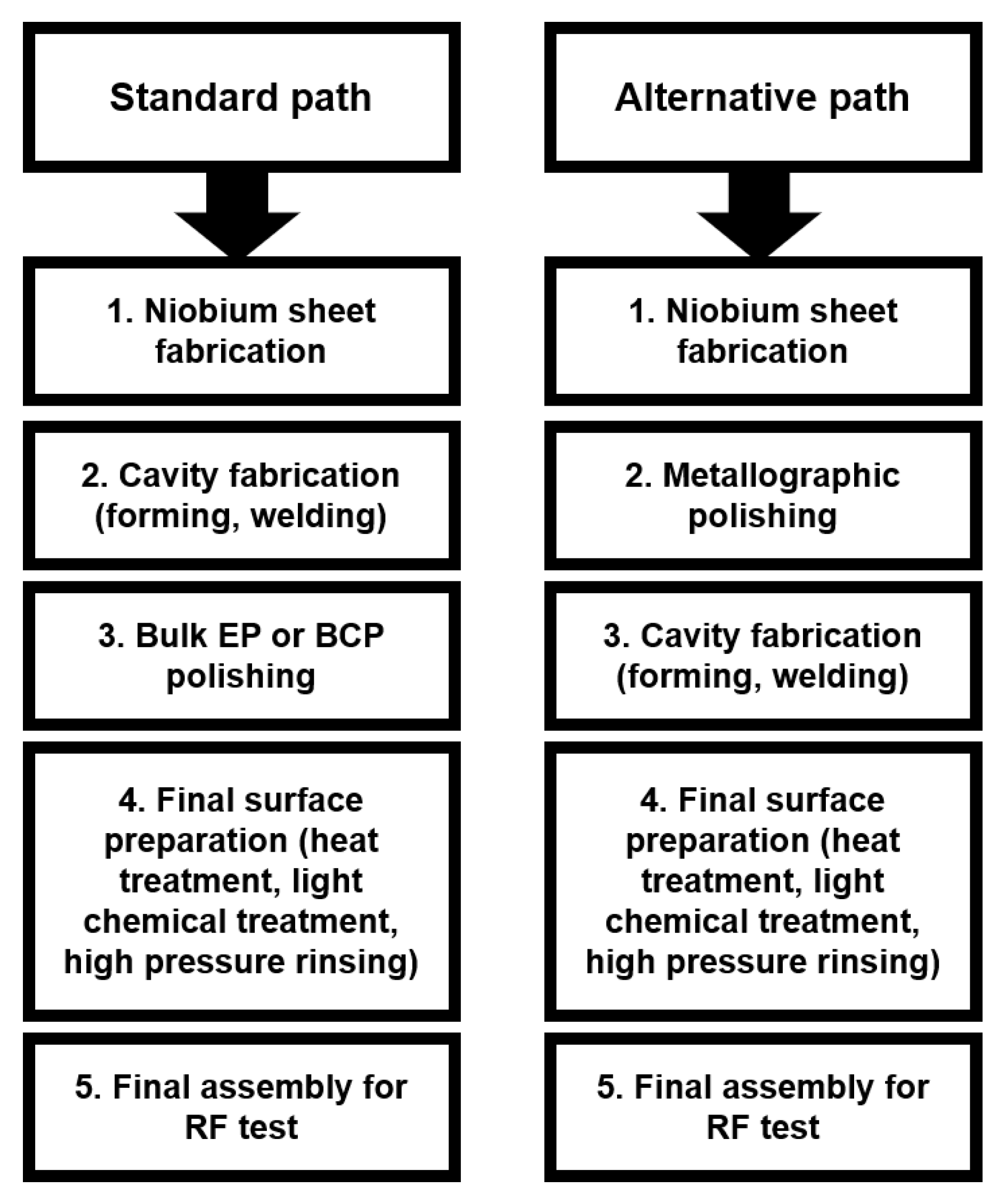
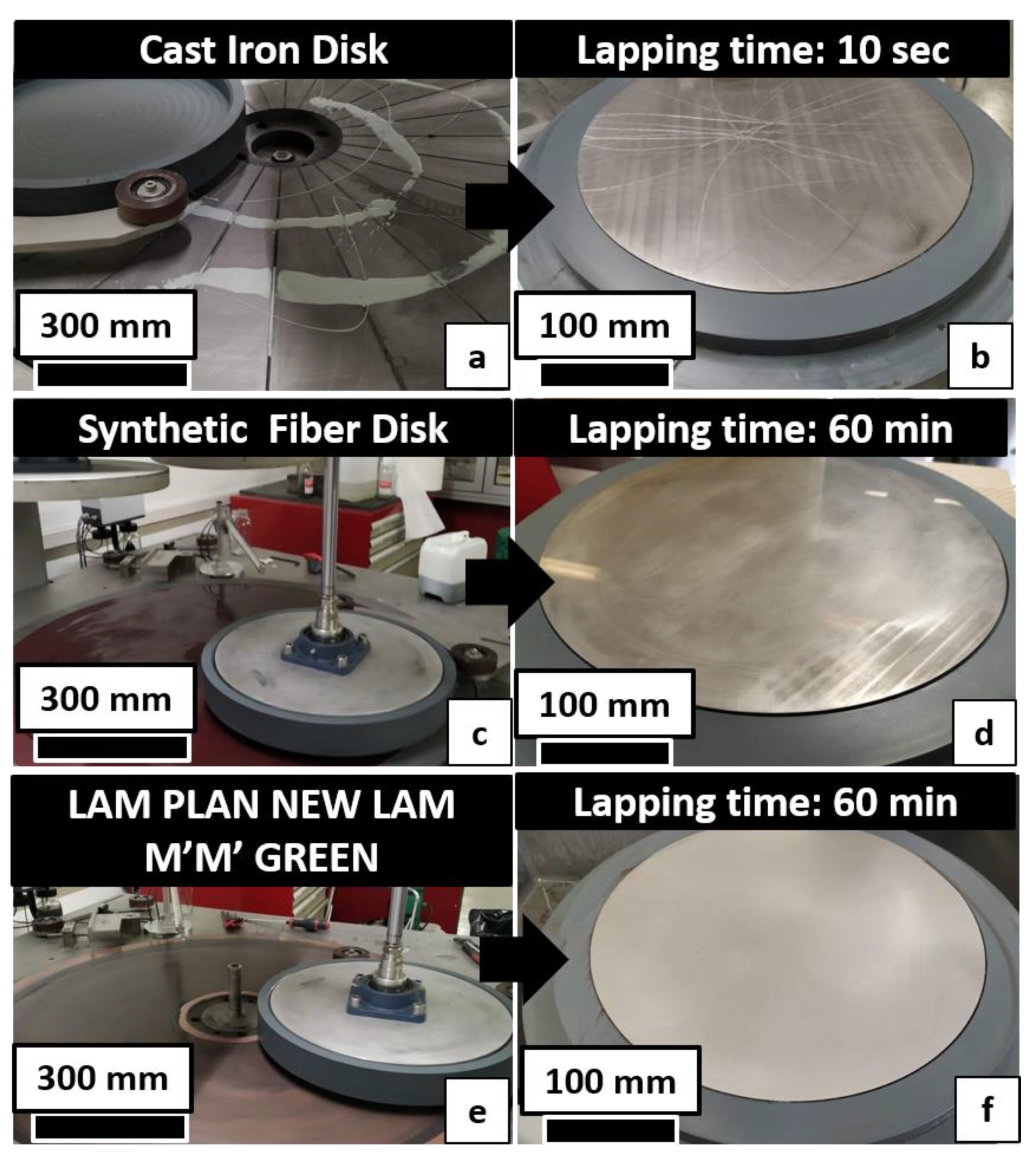
2.3. Metallographic Polishing (MP) Procedure on Large Disks
3. Results and Discussion
3.1. Surface Analysis on Small Samples
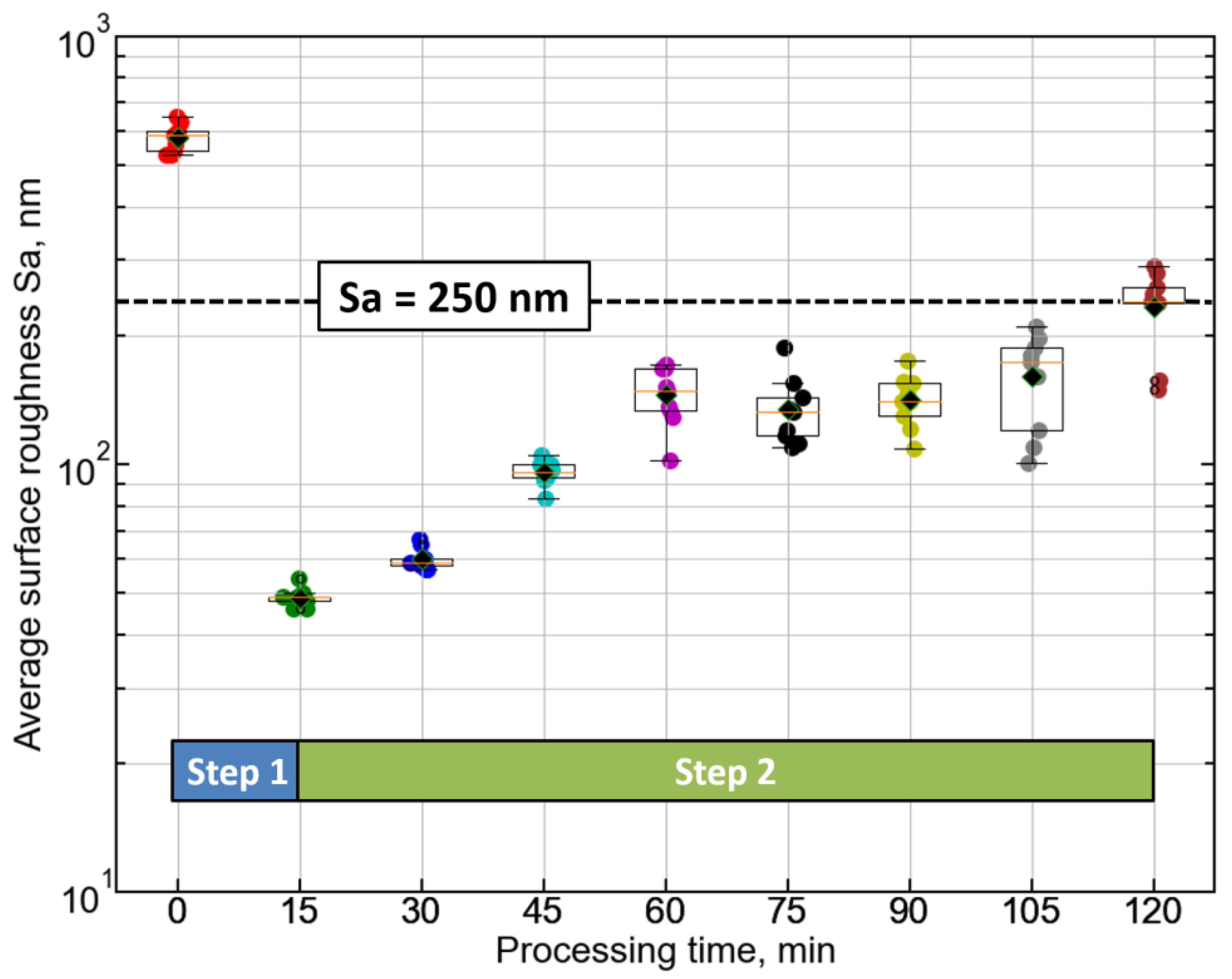
3.1.1. Step 1: Lapping Step
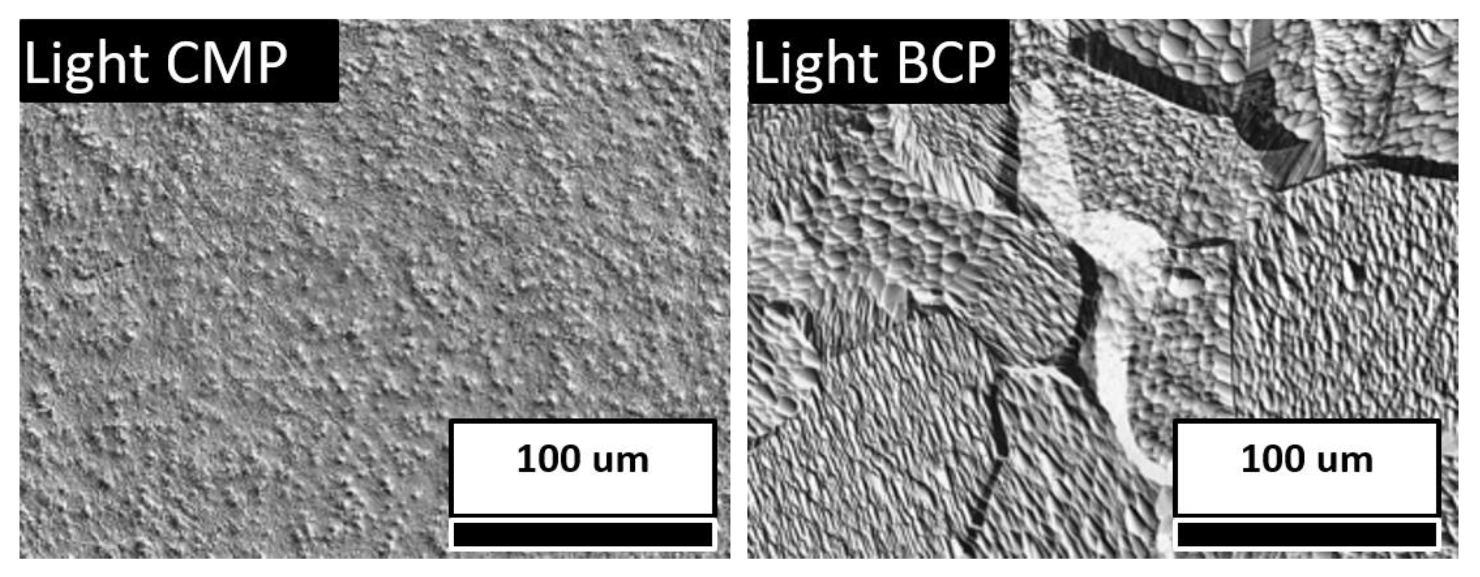
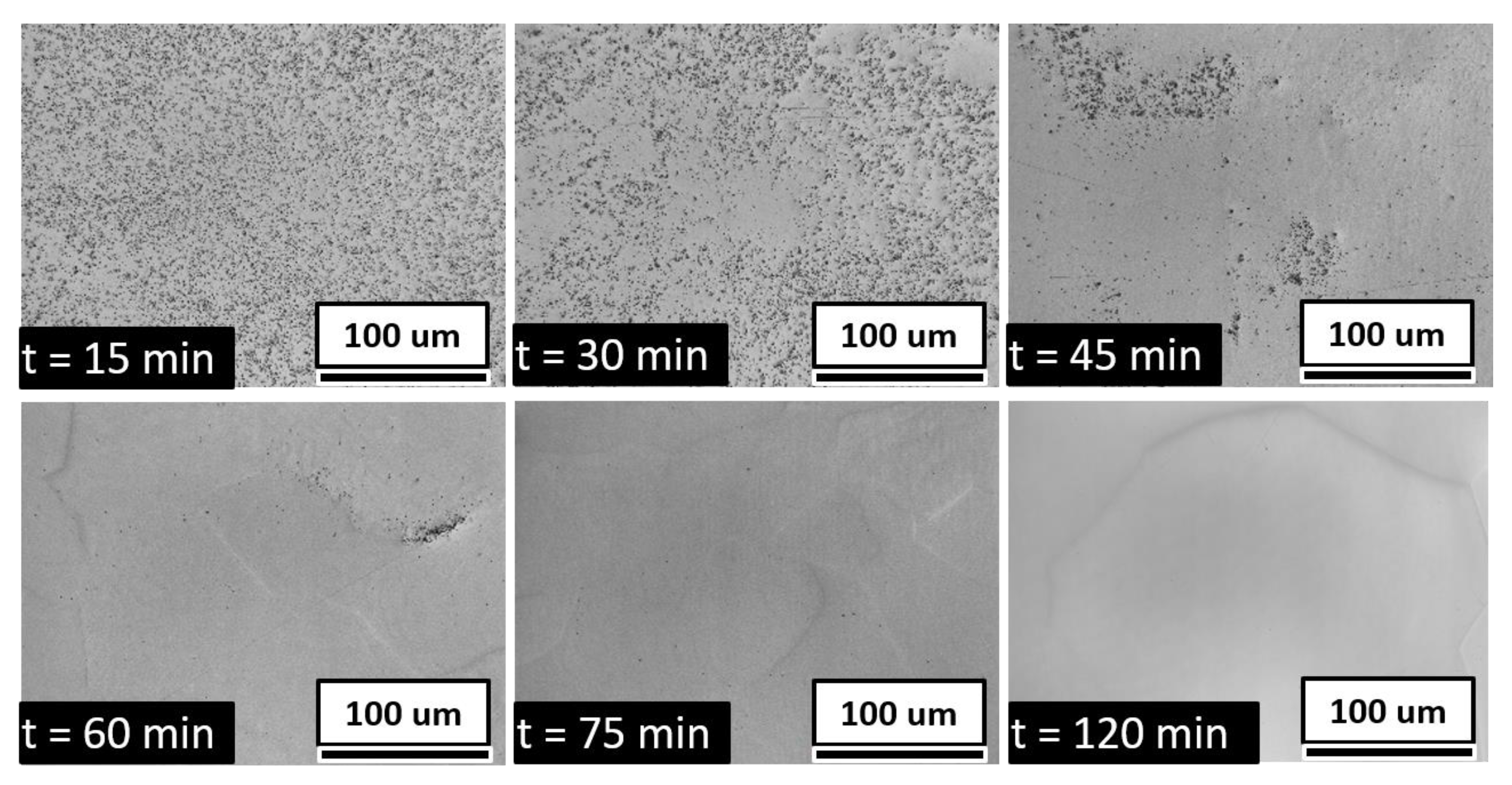
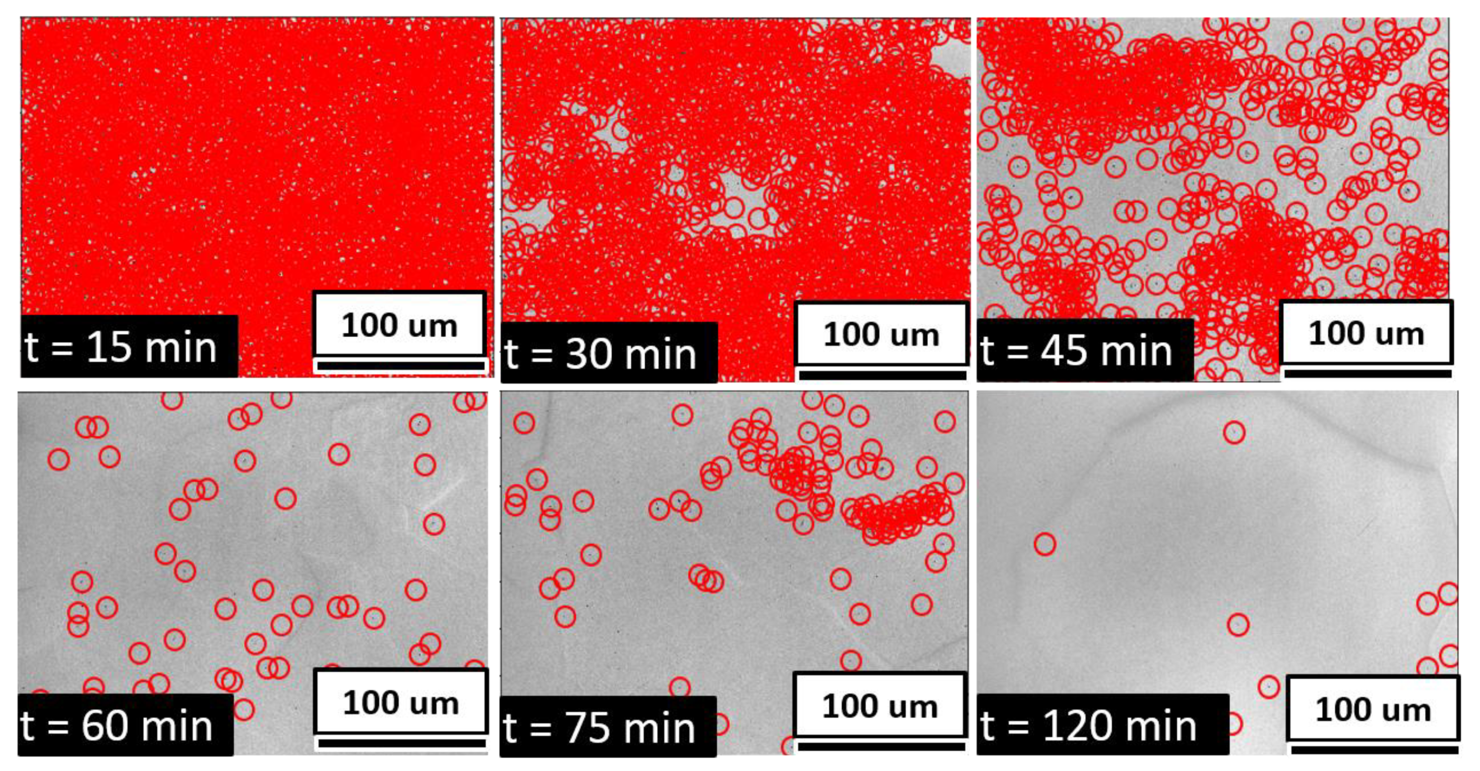
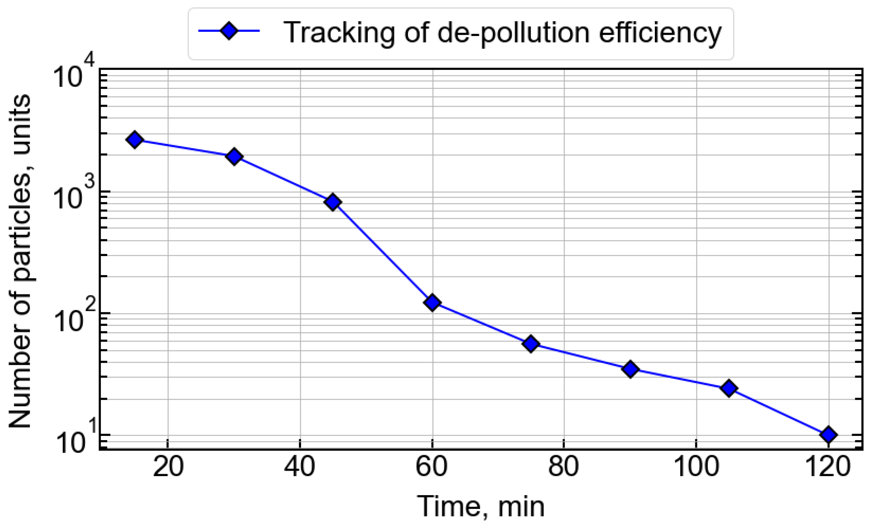
3.1.2. Step 2: Depollution Step
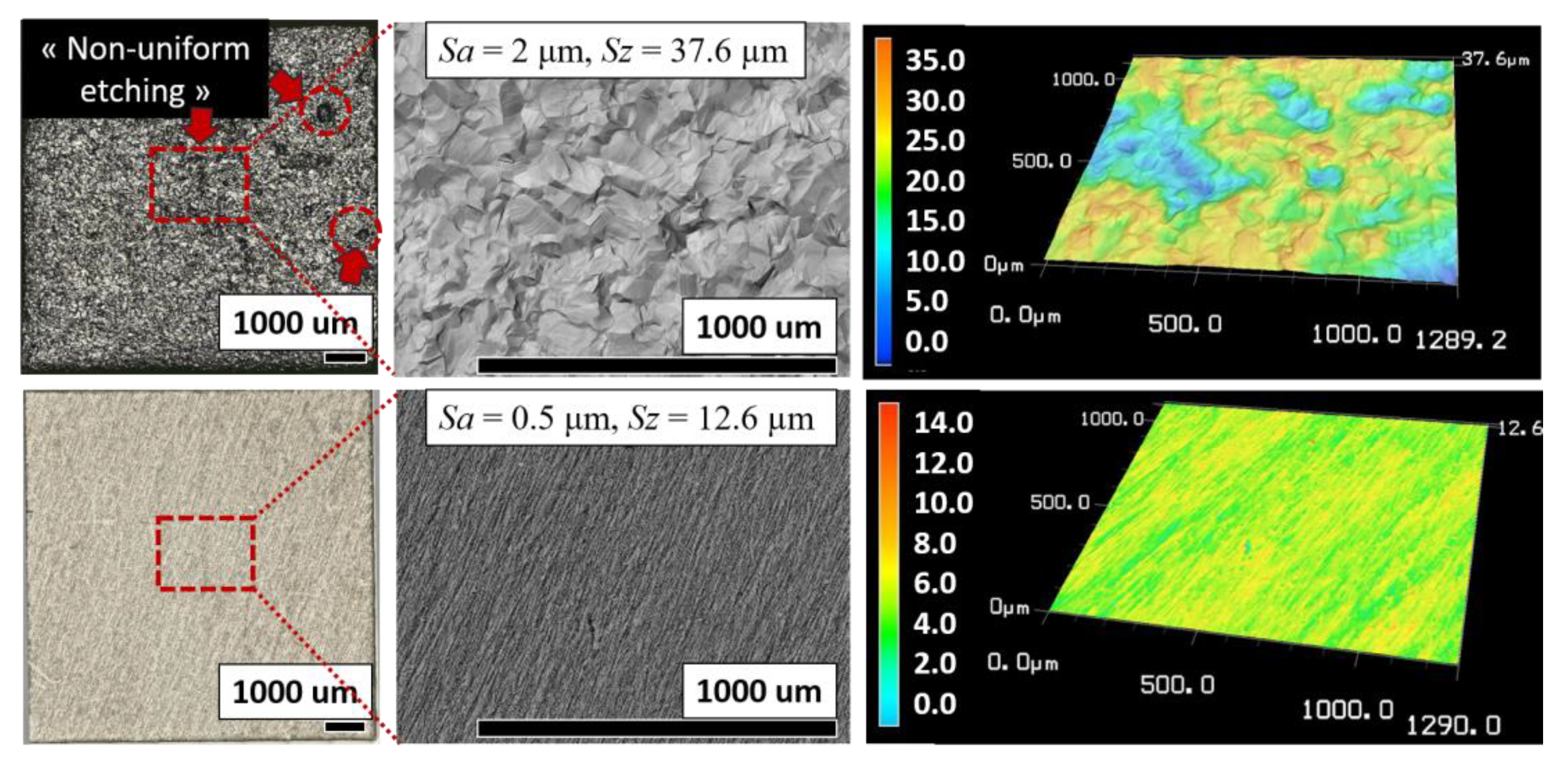
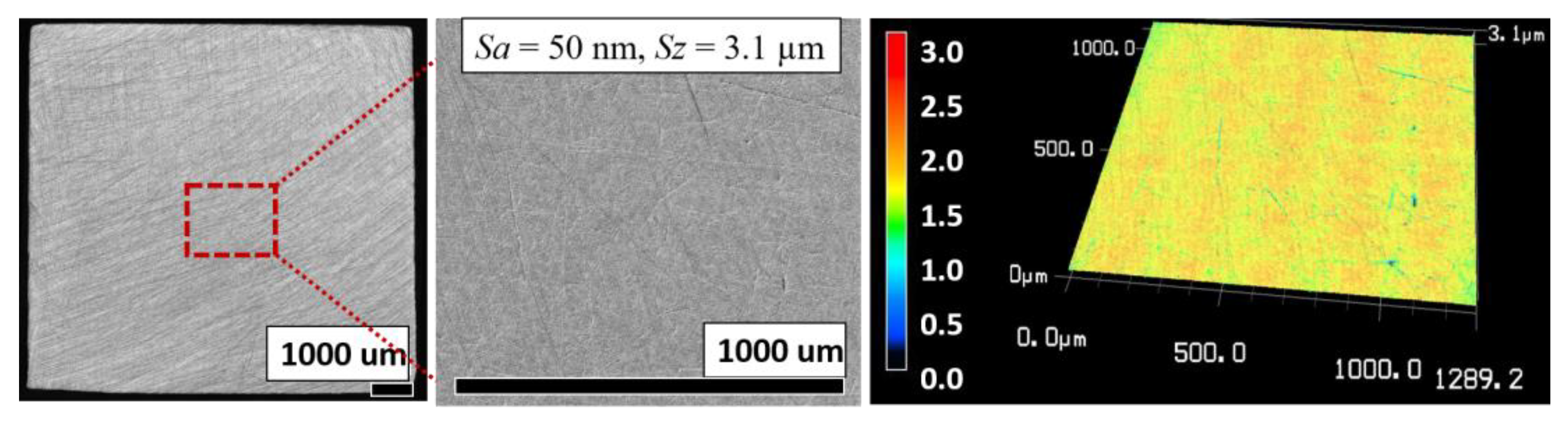
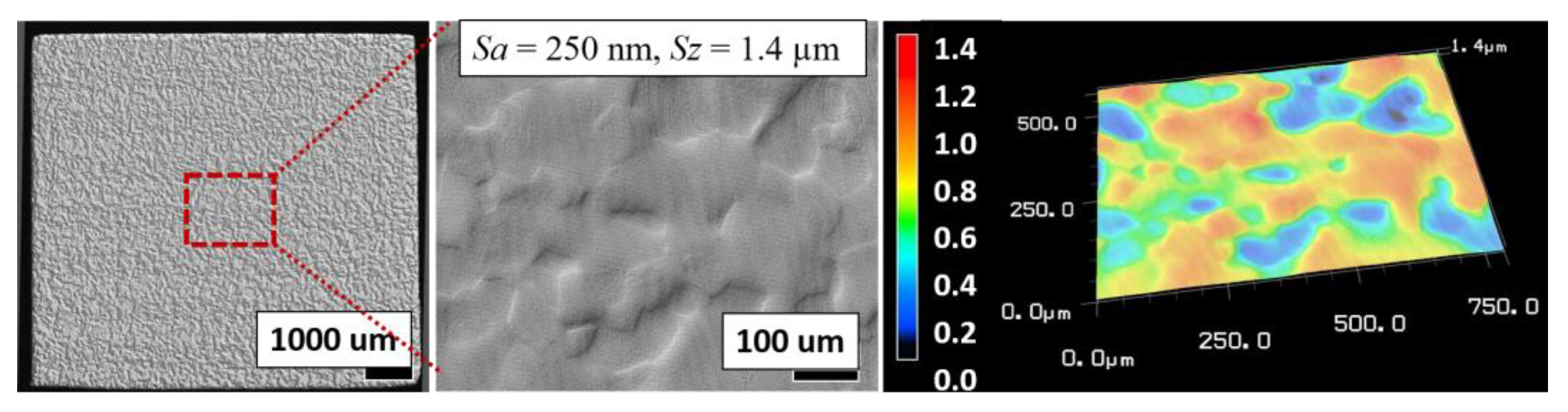
3.2. Final Surface Analysis on Small Samples
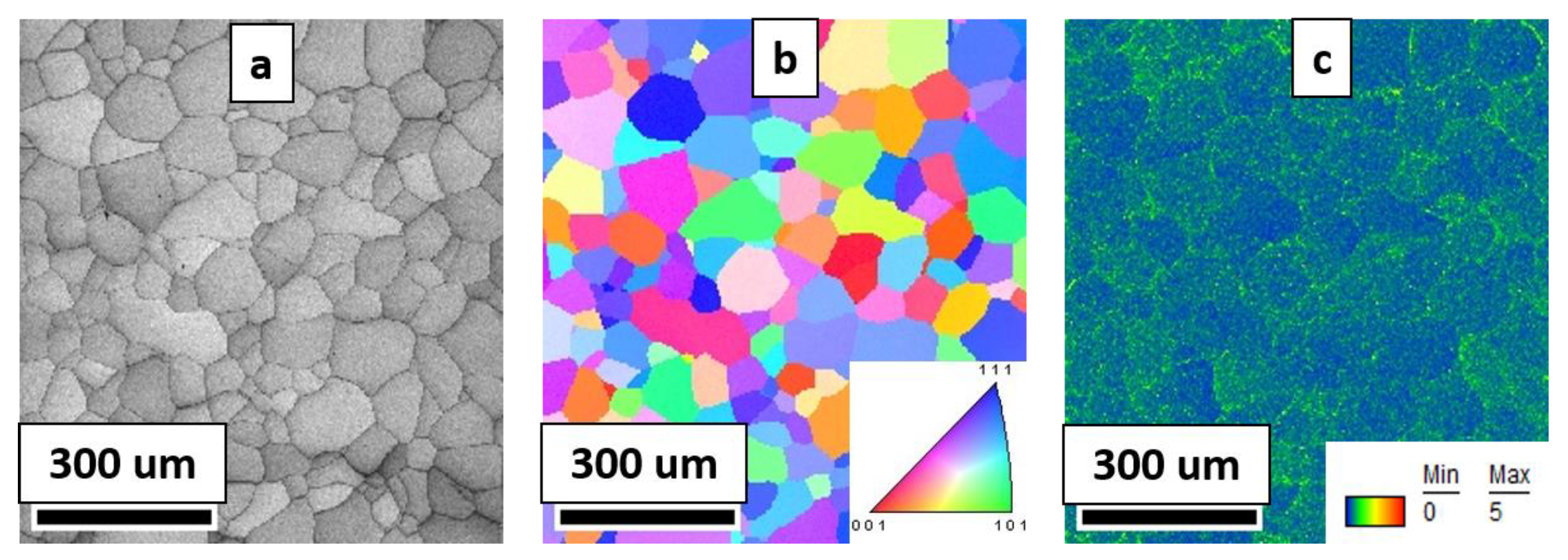
3.2.1. EBSD Analysis
- Blue—no dislocation,
- Green—minor dislocation,
- Red—significant dislocation.
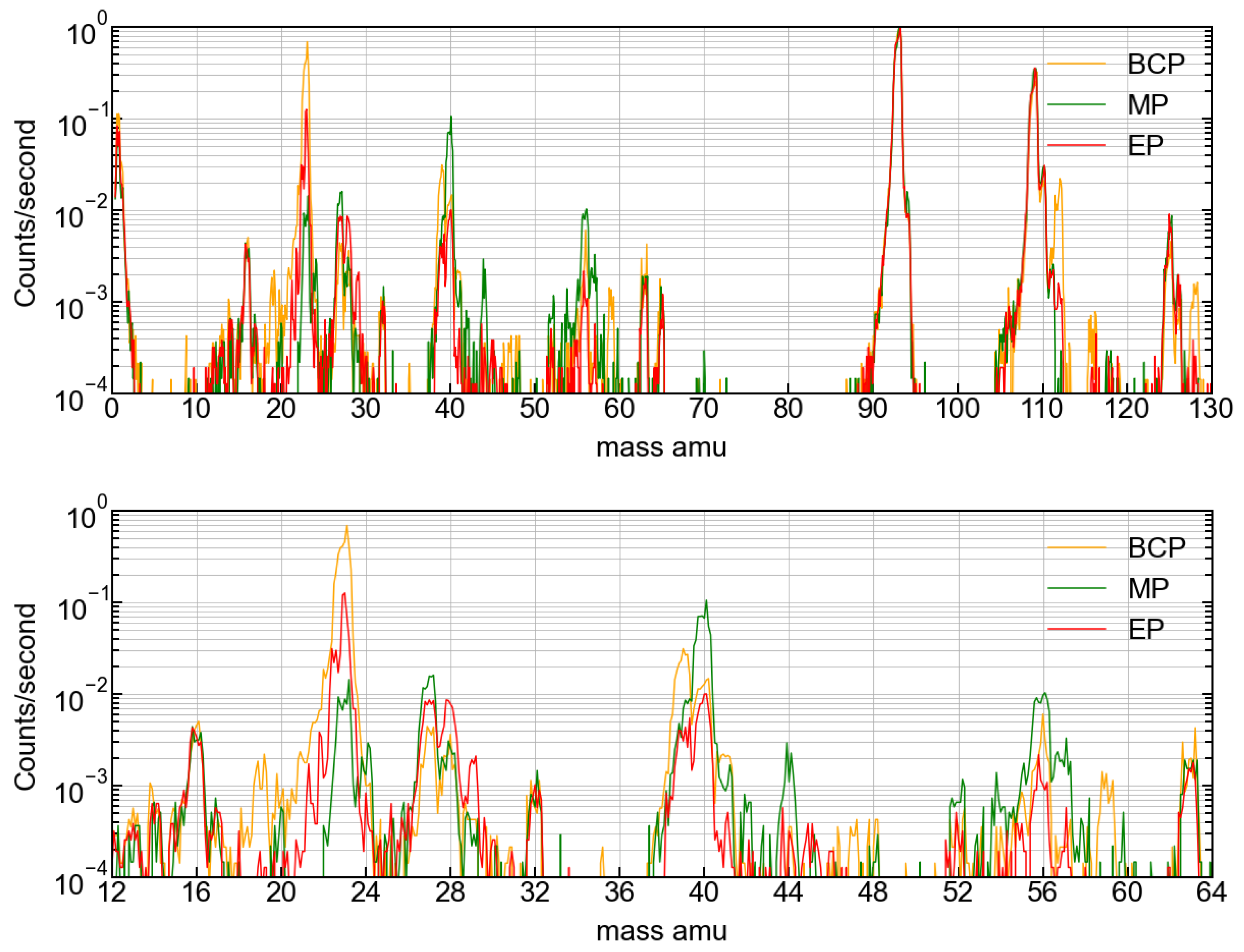
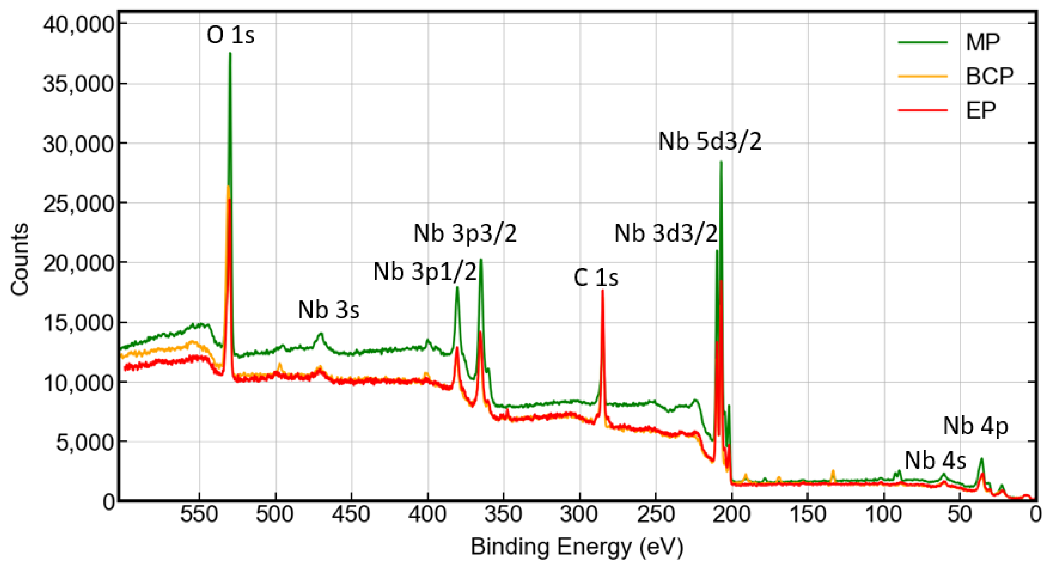
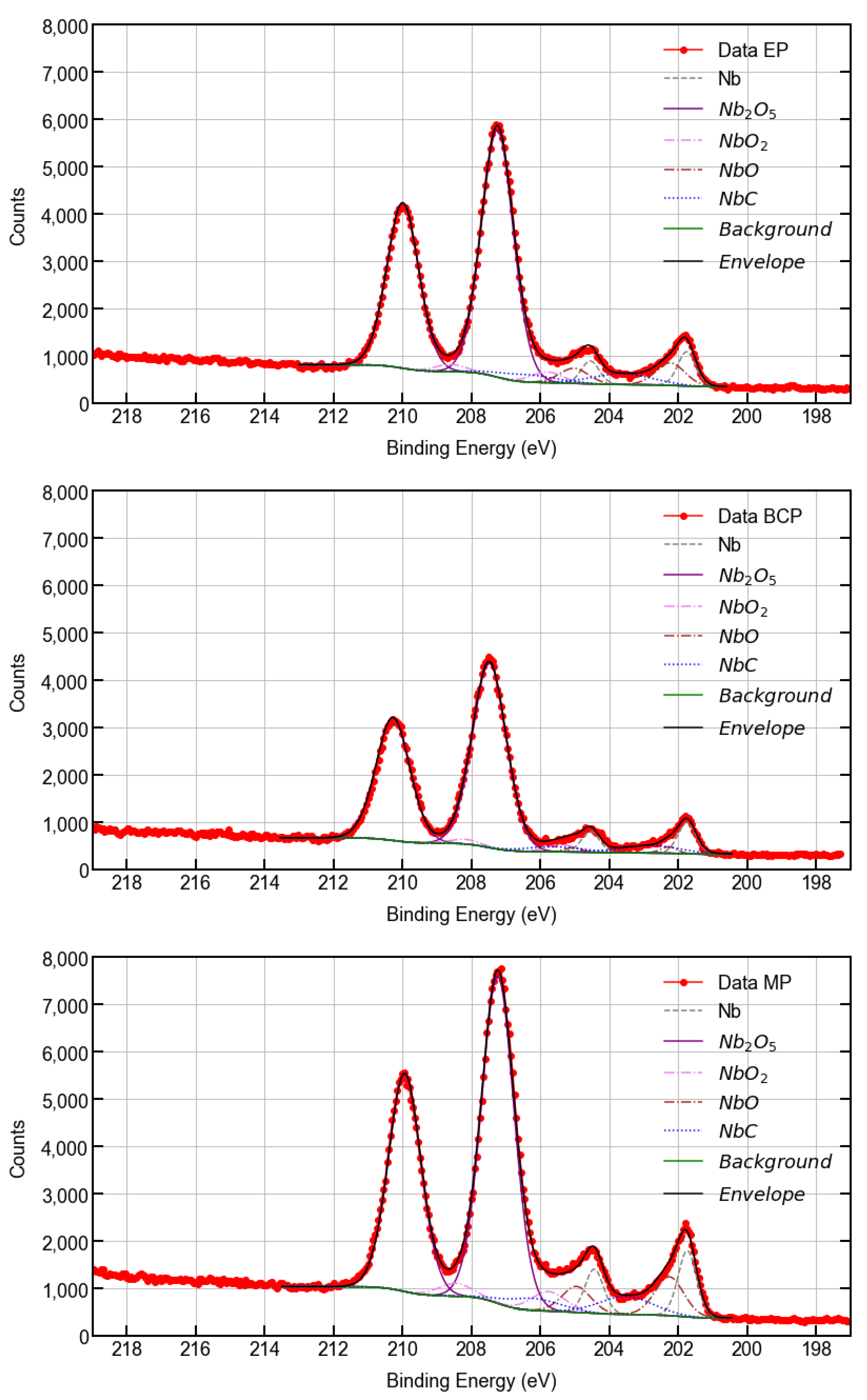
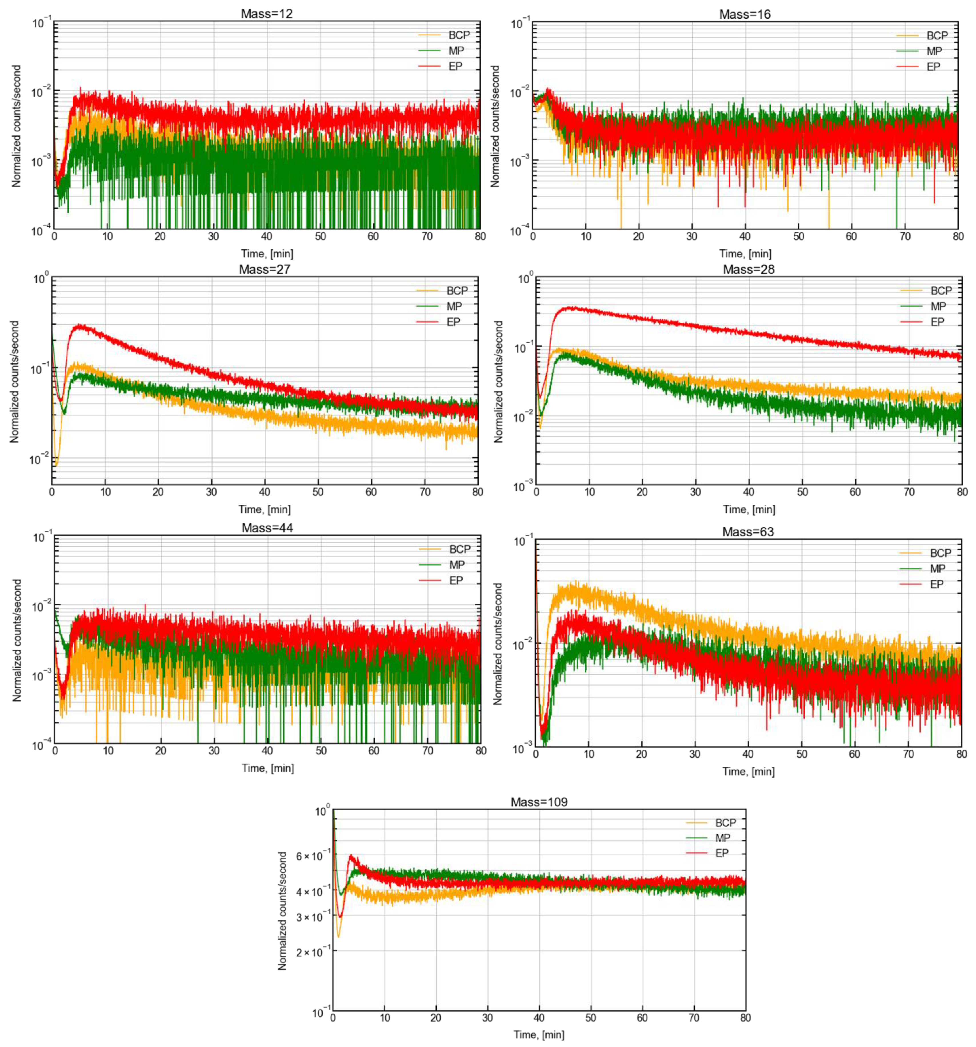
3.2.2. SIMS and XPS Analysis
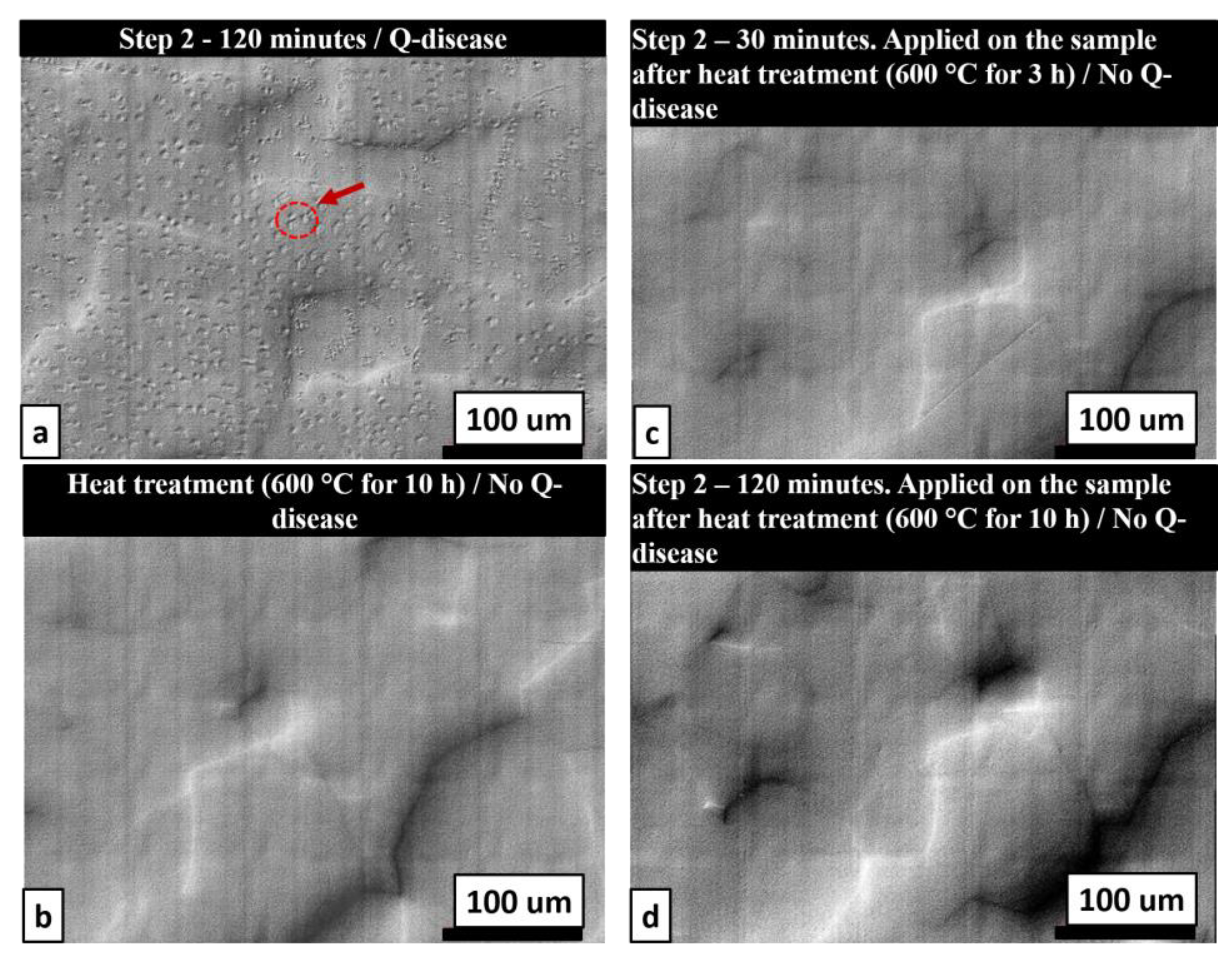
3.2.3. Q-Disease Analysis and Mitigation Treatments
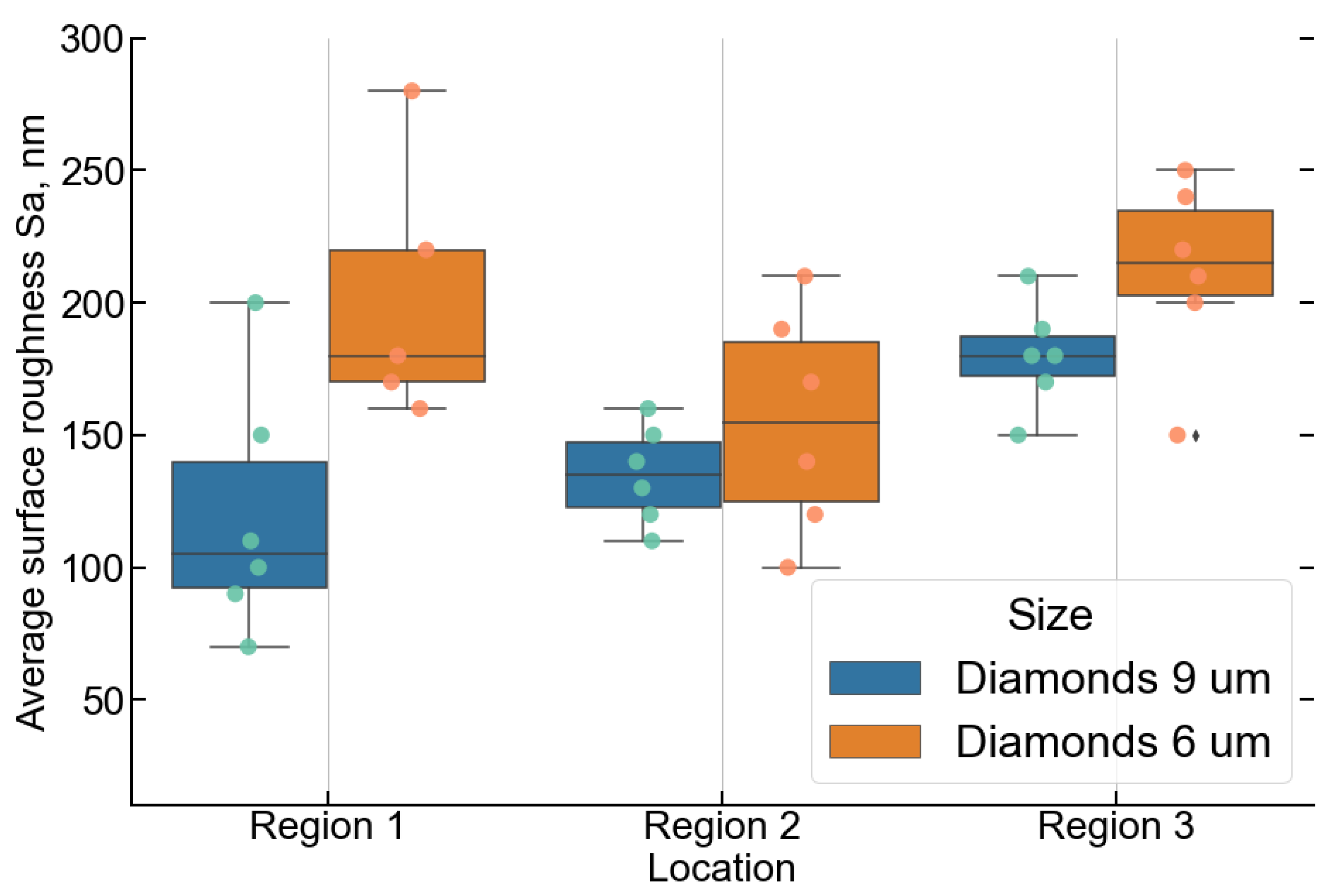
3.3. Transfer to Large Dimensions
3.3.1. Optimization of Step-1 for Large Disks
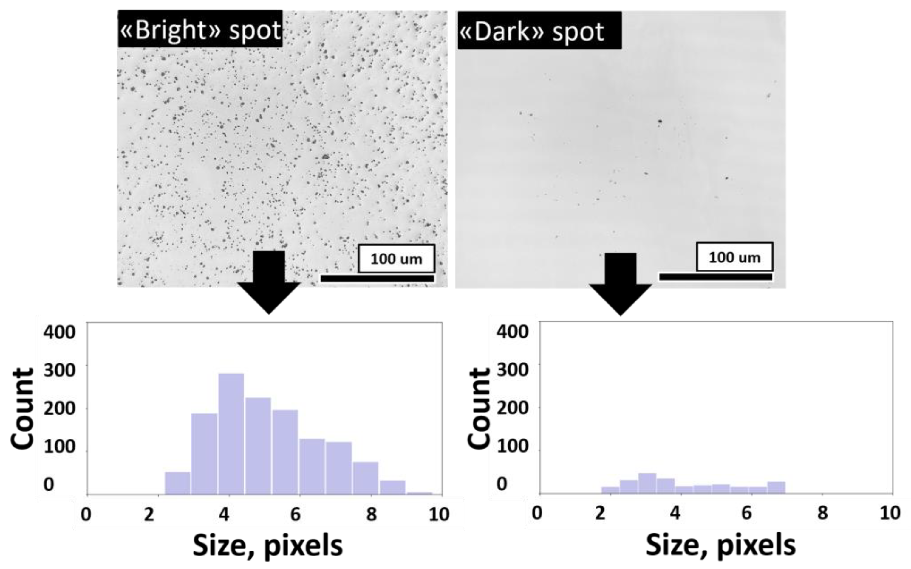
3.3.2. Observed Issue during Step-2 for Large Disks
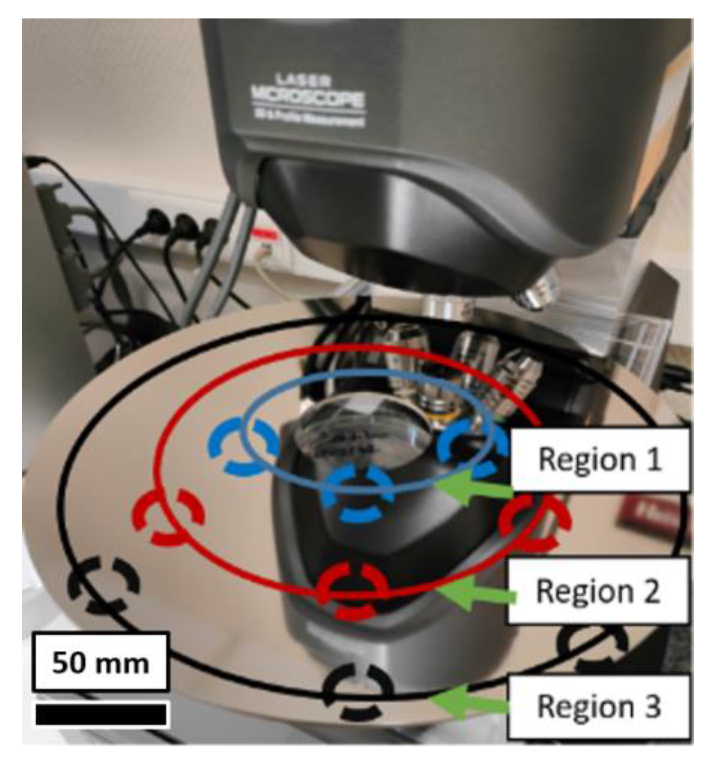
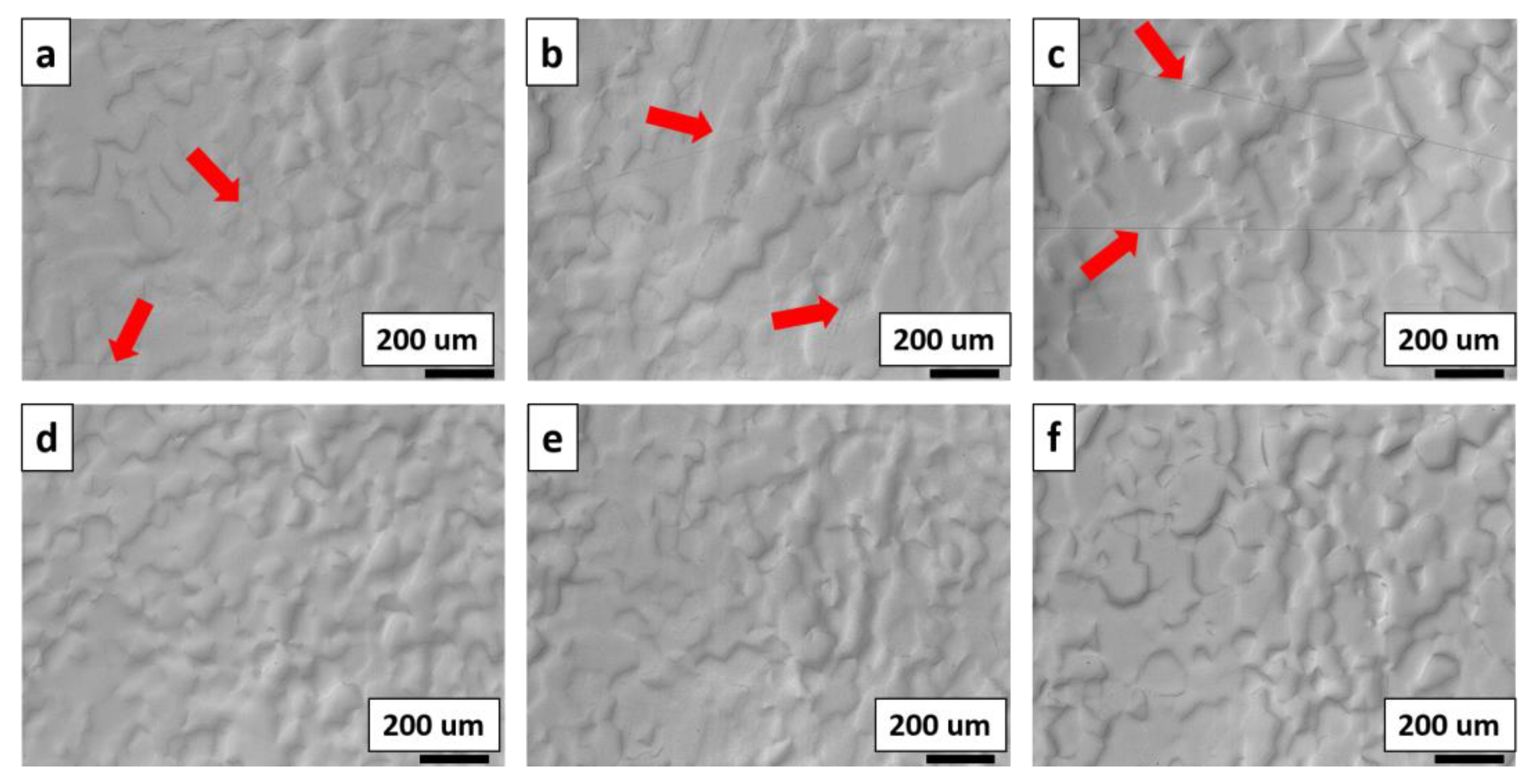
3.3.3. Final Surface Analysis of Large Disk
4. Conclusions
Author Contributions
Funding
Data Availability Statement
Acknowledgments
Conflicts of Interest
Appendix A

References
- Antoine, C. Materials and Surface Aspects in the Development of SRF Niobium Cavities. 2012. Available online: https://cds.cern.ch/record/1472363 (accessed on 25 February 2023).
- Hryhorenko, O.; Antoine, C.Z.; Dohmae, T.; Magnin, W.; Longuevergne, D. Alternative Surface Processing Pathway to the Future Large-Scale Facilities; French-Ukrainian Workshop: Orsay, France, 2021. [Google Scholar]
- Slimani; Hannachi, E. Superconducting Materials: Fundamentals, Synthesis and Applications; Springer Nature: Berlin/Heidelberg, Germany, 2022. [Google Scholar]
- Anlage, S.M. Microwave superconductivity. IEEE J. Microw. 2021, 1, 389–402. [Google Scholar] [CrossRef]
- Parajuli, I.P. Characterization of Losses in Superconducting Radio-Frequency Cavities by Combined Temperature and Magnetic Field Mapping. 2022. Available online: https://www.proquest.com/open-view/a051a501b5352397a83cf03382ddaa70/1?pq-origsite=gscholar&cbl=18750&diss=y (accessed on 25 February 2023).
- Antoine, C.; Valente-Feliciano, A.M.; Anlage, S.; Ciovati, G.; Delayen, J.; Gerigk, F.; Gurevich, A.; Junginger, T.; Keckert, S.; Keppe, G.; et al. Next-Generation Superconducting RF Technology based on Advanced Thin Film Technologies and Innovative Materials for Accelerator Enhanced Performance and Energy Reach. arXiv 2022, arXiv:2204.02536. [Google Scholar]
- Junginger, T.; Koscielniak, S.; Satogata, T.; Schaa, V.R.W.; Thomson, J. Critical Fields of SRF Materials. In Proceedings of the 9th International Particle Accelerator Conference (IPAC’18), Vancouver, BC, Canada, 29 April–4 May 2018. [Google Scholar]
- Pudasaini, U.; Reece, C.; Rimmer, R.A.; Valente-Feliciano, A.-M.; Barzi, E.J.; Eremeev, G. Next Generation SRF Accelerators Based on Nb3Sn, Snowmass. 2021. Available online: https://indico.fnal.gov/event/47326/contributions/206304/attachments/138987/174297/SNOWMASS21-AF7_AF3_Rimmer-172.pdf (accessed on 25 February 2023).
- Chouhan, V.; Kato, S.; Nii, K.; Yamaguchi, T.; Sawabe, M.; Saeki, T.; Monjushiro, H.; Oikawa, H.; Ito, H.; Hayano, H.; et al. Vertical electropolishing for 1.3 GHz single-and nine-cell superconducting niobium cavities: A parametric optimization and rf performance. Phys. Rev. Accel. Beams 2019, 22, 103101. [Google Scholar] [CrossRef] [Green Version]
- Demercastel-Soulier, J.; Duchesne, P.; Longuevergne, D.; Olry, G.; Pépin-Donat, T.; Rabehasy, F.; Roset, S.; Vogt, L. Improvement of Chemical Etching Capabilities (BCP) for SRF Spoke Resonators at IJCLab. In Proceedings of the 20th International Conference on RF Superconductivity, East Lansing, MI, USA, 28 June–2 July 2021. [Google Scholar]
- Hryhorenko, O. Development and Optimization of Mechanical Polishing Process for Superconducting Accelerating Cavities. Ph.D. Thesis, Université Paris-Saclay, Orsay, France, 2019. [Google Scholar]
- Pira, C.; Chyhyrynets, E.; Stivanello, F.; Caforio, R. Plasma Electrolytic Polishing as a promising treatment replacement of electropolishing in the copper and Niobium substrate preparation for SRF. In Proceedings of the 9th International Workshop on Thin Films and New Ideas for Pushing the Limits of RF Superconductivity, Online, 15–18 March 2021. [Google Scholar]
- Hryhorenko, O.; Antoine, C.Z.; Chabot, M.; Longuevergne, D. Metallographic polishing pathway to the future of large scale SRF facilities. In Proceedings of the 19th International Conference on RF Superconductivity (SRF’19), Dresden, Germany, 30 June–5 July 2019. [Google Scholar]
- Peshl, J.J. Characterization of Argon and Ar/Cl 2 Plasmas Used for the Processing of Niobium Superconducting Radio-Frequency Cavities; Old Dominion University: Norfolk, VA, USA, 2019. [Google Scholar]
- Furuta, F.; Ring, T. Cavity Processing Laboratory for SRF Cavities; Fermi National Accelerator Lab. (FNAL): Batavia, IL, USA, 2020. [Google Scholar]
- Popielarski, L. Cavity Processing and Cleanroom Techniques. In Proceedings of the 19th International Conference on RF Superconductivity (SRF’19), Dresden, Germany, 30 June–5 July 2019. [Google Scholar]
- Tamashevich, Y. Diagnostics and Treatment of 1.3 GHz Nb Cavities. Ph.D. Thesis, Universität Hamburg, Hamburg, Germany, 2017. [Google Scholar] [CrossRef]
- Trubacova, P.; Atieh, S.; Bajard, F.; Terricabras, A.; Rosaz, G.; Rigaud, J. Niobium micro-mechanical polishing for superconductive radio-frequency applications. In Proceedings of the Euspen’S 20th International Conference & Exhibition, Geneva, Switzerland, 8–12 June 2020. [Google Scholar]
- Cooper, C.A.; Cooley, L.D. Mirror-smooth surfaces and repair of defects in superconducting RF cavities by mechanical polishing. Supercond. Sci. Technol. 2012, 26, 015011. [Google Scholar] [CrossRef] [Green Version]
- Navitski, A.; Foster, B.; Prudnikava, A.; Tamashevich, Y. Surface analyses and optimization of centrifugal barrel polishing of Nb cavities. In Proceedings of the SRF2015, Whistler, BC, Canada, 13–18 September 2015. [Google Scholar]
- Porshyn, V.; Serbun, P.; Bürger, H.; Soykarci, S.; Lützenkirchen-Hecht, D. Laser treatment of niobium surfaces for SRF applications. J. Phys. Conf. Ser. IOP Publ. 2018, 1067, 082011. [Google Scholar] [CrossRef]
- Calota, G.; Maximova, N.; Ziemer, K.S.; Müftü, S. Investigation of chemical/mechanical polishing of niobium. Tribol. Trans. 2009, 52, 447–459. [Google Scholar] [CrossRef]
- Antoine, C.; Crooks, R. Reducing electropolishing time with chemical-mechanical polishing. In Proceedings of the SRF2009, Berlin, Germany, 20–25 September 2009; p. 405. [Google Scholar]
- Hryhorenko, O.; Antoine, C.Z.; Dohmae, T.; Brisset, F.; Longuevergne, D. Investigation of an Alternative Path for SRF Cavity Fabrication and Surface Processing. In Proceedings of the SRF 2021, East Lansing, MI, USA, 28 June–2 July 2022; pp. 319–322. [Google Scholar]
- Geels, K. (Ed.) Metallographic and Materialographic Specimen Preparation, Light Microscopy, Image Analysis, and Hardness Testing; ASTM International: West Conshohocken, PA, USA, 2007; Volume 46. [Google Scholar]
- Liu, D.; Zhang, Z.; Feng, J.; Yu, Z.; Meng, F.; Xu, G.; Wang, J.; Wen, W.; Liu, L. Atomic-level flatness on oxygen-free copper surface in lapping and chemical mechanical polishing. Nanoscale Adv. 2022, 4, 4263–4271. [Google Scholar] [CrossRef] [PubMed]
- Mittal, M.; Verma, A.; Kaur, I.; Kaur, B.; Sharma, M.; Goyal, L.M.; Roy, S.; Kim, T.-H. An efficient edge detection approach to provide better edge connectivity for image analysis. IEEE Access 2019, 7, 33240–33255. [Google Scholar] [CrossRef]
- Szeliski, R. Computer Vision: Algorithms and Applications; Springer Nature: Berlin/Heidelberg, Germany, 2022. [Google Scholar]
- Padamsee, H. History of gradient advances in SRF. arXiv 2020, arXiv:2004.06720. [Google Scholar]
- Jung, Y.; Lee, J.; Lee, S.; Kim, J.; Choi, B.; Kim, H.; Joo, J.; Kim, Y.; Jung, H. Heat Treatment for a Prototype Half-Wave Resonator Cavity. In Proceedings of the 29th Linear Accelerator Conference-LINAC18, Beijing, China, 16–21 September 2018. [Google Scholar]
- Wang, M.; Polyanskii, A.; Balachandran, S.; Chetri, S.; Crimp, M.; Lee, P.; Bieler, T. Investigation of the effect of structural defects from hydride precipitation on superconducting properties of high purity SRF cavity Nb using magneto-optical and electron imaging methods. Supercond. Sci. Technol. 2022, 35, 045001. [Google Scholar] [CrossRef]
- Keckert, S.; Kleindienst, R.; Kugeler, O.; Tikhonov, D.; Knobloch, J. Characterizing materials for superconducting radiofrequency applications—A comprehensive overview of the quadrupole resonator design and measurement capabilities. Rev. Sci. Instrum. 2021, 92, 064710. [Google Scholar] [CrossRef] [PubMed]
- Monroy-Villa, R.; Zadeh, S.G.; Hillert, W.; Putek, P.; Reschke, D.; Thie, J.-H.; Wenskat, M. Design and Fabrication of a Quadrupole Resonator for SRF R&D. In Proceedings of the 12th International Particle Accelerator Conference (IPAC 2021), Online, 24–28 May 2021. [Google Scholar]
- Sundahl, C.; Makita, J.; Welander, P.B.; Su, Y.-F.; Kametani, F.; Xie, L.; Zhang, H.; Li, L.; Gurevich, A. Development and characterization of Nb3Sn/Al2O3 superconducting multilayers for particle accelerators. Sci. Rep. 2021, 11, 7770. [Google Scholar] [CrossRef] [PubMed]
- Martinet, G. Results on bulk Niobium surface resistance measurement with pillbox cavity on TE011/TE012 modes. In Proceedings of the 19th International Conference on RF Superconductivity, Dresden, Germany, 30 June–5 July 2019. [Google Scholar]
- Carneiro, Í.; Simões, S. Recent advances in EBSD characterization of metals. Metals 2020, 10, 1097. [Google Scholar] [CrossRef]
- CasaXPS: Processing Software for XPS, AES, SIMS and More. Available online: http://www.casaxps.com (accessed on 25 February 2023).
- NIST X-ray Photoelectron Spectroscopy Database. Available online: https://srdata.nist.gov/xps/Default.aspx (accessed on 25 February 2023).
- Major, G.H.; Fairley, N.; Sherwood, P.M.A.; Linford, M.R.; Terry, J.; Fernandez, V.; Artyushkova, K. Practical guide for curve fitting in x-ray photoelectron spectroscopy. J. Vac. Sci. Technol. A 2020, 38, 061203. [Google Scholar] [CrossRef]
- Murakami, R.; Kageyama, H.; Nakamura, K.; Tanaka, H.; Shinotsuka, H.; Yoshikawa, H.; Yoshihara, K. Background Estimation in X-ray Photoelectron Spectroscopy Data Using an Active Shirley Method with Automated Selection of the Analytical Range. e-J. Surf. Sci. Nanotechnol. 2019, 17, 61–68. [Google Scholar] [CrossRef] [Green Version]
- Fouaidy, M.; Chatelet, F.; Le Drean, D.; Longuevergne, D.; Martret, R.; Olry, G.; Pepin-Donat, T.; Proslier, T.; Maurice, L. Recent Results of High Temperature Vacuum Heat Treatment Program of SRF Resonators at IJCLab. IEEE Trans. Appl. Supercond. 2021, 31, 1–8. [Google Scholar] [CrossRef]
- Wenskat, M.; Bate, C.; Reschke, D.; Weise, H.; Butterling, M.; Hirschmann, E.; Liedke, M.; Wagner, A. Vacancy-Hydrogen Dynamics in Samples During Low Temperature Baking. In Proceedings of the 19th International Conference on RF Superconductivity (SRF’19), Dresden, Germany, 30 June–5 July 2019; JACOW Publishing: Geneva, Switzerland, 2019. [Google Scholar]
- Prudnikava, A.; Tamashevich, Y.; Yanushkevich, K.; Noei, H.; Lott, D.; Stierle, A.; Foster, B. Toward Optimization of Centrifugal Barrel Polishing Procedure for Treatment of Niobium Cavities. IEEE Trans. Appl. Supercond. 2018, 28, 1–5. [Google Scholar] [CrossRef]
- Semione, G.D.L.; Vonk, V.; Pandey, A.D.; Grånäs, E.; Arndt, B.; Wenskat, M.; Hillert, W.; Noei, H.; Stierle, A. Temperature-dependent near-surface interstitial segregation in niobium. J. Phys. Condens. Matter 2021, 33, 265001. [Google Scholar] [CrossRef] [PubMed]


| Mass, amu | 1 | 14 | 16 | 23 | 27 | 28 | 39 | 40 | 44 | 56 | 63 | 93 | 109 | 125 |
|---|---|---|---|---|---|---|---|---|---|---|---|---|---|---|
| Species | H+ | CH2+, N+, | O+, CH4+ | Na+ | Al+, C2H3+ | Si+, CO+, N2+, C2H4+ | K+, C3H3+ | Ca+, Ar+ | SiO+ | Fe+, Si2+ | Cu+, ClSi+ | Nb+ | NbO+ | NbO2+ |
| Polishing | Element | Composition and Chemical States | |||||
|---|---|---|---|---|---|---|---|
| BCP | Nb 3d5/2, Nb 3d3/2 | Nb2O5 | NbO2 | NbO | Nb | NbC | |
| Binding energy [eV] | 207.48, 210.28 | 205.39, 208.19 | 202.27, 205.07 | 201.74, 204.54 | 202.79, 205.59 | ||
| FWHM [eV] | 1.16 | 1 | 0.55 | 0.61 | 2.04 | ||
| Composition [%] | 82.55 | 2.75 | 1.35 | 7.38 | 5.97 | ||
| EP | Nb 3d5/2, Nb 3d3/2 | Nb2O5 | NbO2 | NbO | Nb | NbC | |
| Binding energy [eV] | 207.24, 209.99 | 205.8, 208.6 | 202.22, 205.02 | 201.75, 204.55 | 203.63, 206.43 | ||
| FWHM [eV] | 1.09 | 1.08 | 0.99 | 0.61 | 2.02 | ||
| Composition [%] | 77.82 | 3.31 | 6.43 | 6.03 | 6.4 | ||
| MP | Nb 3d5/2, Nb 3d3/2 | Nb2O5 | NbO2 | NbO | Nb | NbC | |
| Binding energy [eV] | 207.23, 209.93 | 205.76, 208.46 | 202.25, 204.95 | 201.73, 204.43 | 203.52, 206.22 | ||
| FWHM [eV] | 1.11 | 1.17 | 0.98 | 0.63 | 1.8 | ||
| Composition [%] | 73.07 | 4.51 | 7.6 | 8.38 | 6.43 | ||
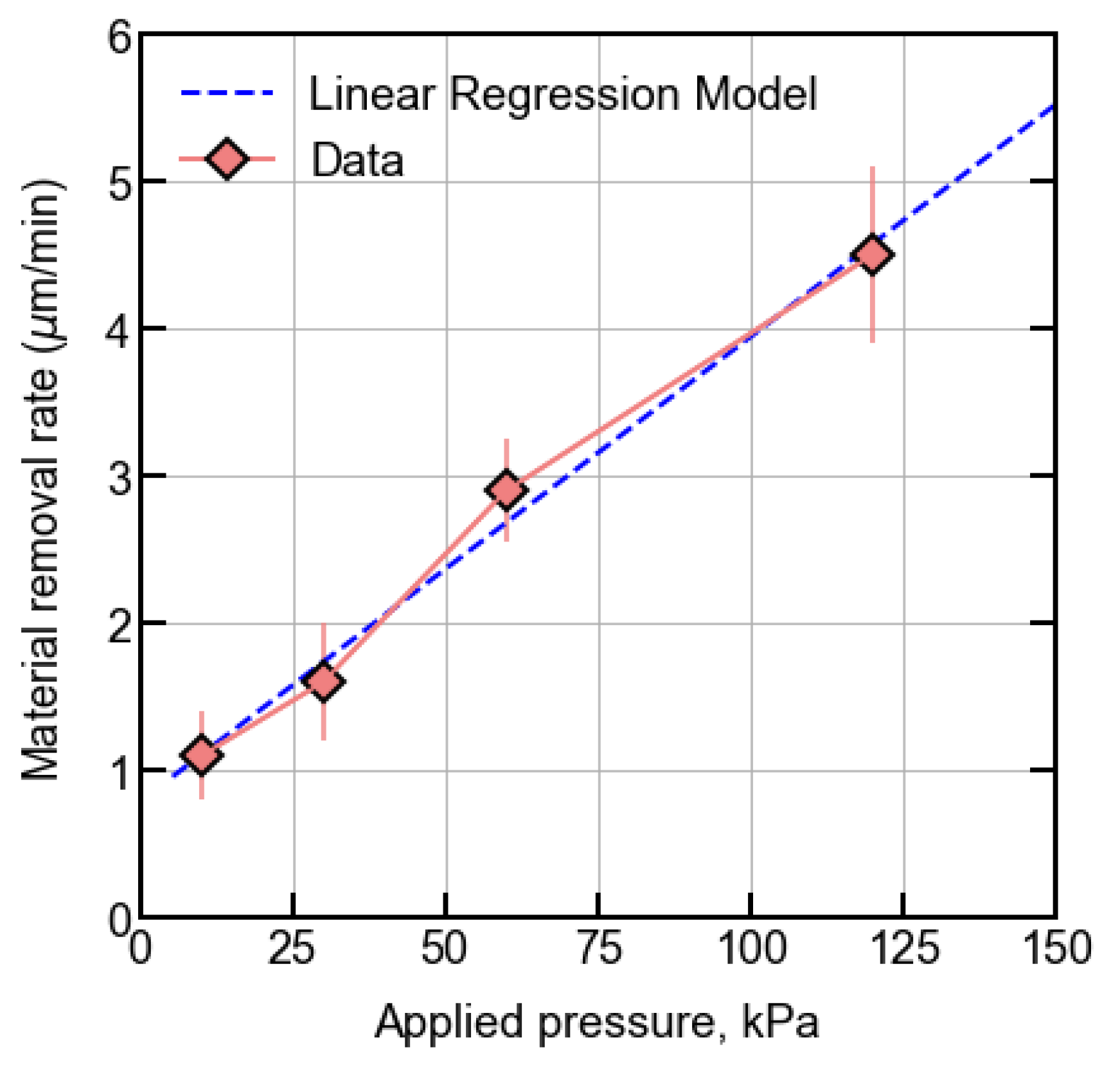
| Disk Type + Diamonds, µm | MRR, µm/min | ||
|---|---|---|---|
| 1 | 1200 | CAMEO Gold + 3 | 4.5 ± 0.6 |
| 1 | 600 | CAMEO Gold + 3 | 2.9 ± 0.4 |
| 1 | 300 | CAMEO Gold + 3 | 1.6 ± 0.4 |
| 1 | 200 | CAMEO Gold + 3 | 1.1 ± 0.3 |
| 125 | 100 | CAMEO Gold + 3 | 0.6 ± 0.1 |
| 530 | 200 | New Lam M’M’ Green + 6 | 1 ± 0.1 |
| 530 | 200 | New Lam M’M’ Green + 9 | 1.5 ± 0.1 |
Disclaimer/Publisher’s Note: The statements, opinions and data contained in all publications are solely those of the individual author(s) and contributor(s) and not of MDPI and/or the editor(s). MDPI and/or the editor(s) disclaim responsibility for any injury to people or property resulting from any ideas, methods, instructions or products referred to in the content. |
© 2023 by the authors. Licensee MDPI, Basel, Switzerland. This article is an open access article distributed under the terms and conditions of the Creative Commons Attribution (CC BY) license (https://creativecommons.org/licenses/by/4.0/).
Share and Cite
Hryhorenko, O.; Antoine, C.Z.; Magnin, W.; Rajkumar, M.; Brisset, F.; Guilet, S.; Longuevergne, D. An Innovative Approach of Surface Polishing for SRF Cavity Applications. J. Manuf. Mater. Process. 2023, 7, 62. https://doi.org/10.3390/jmmp7020062
Hryhorenko O, Antoine CZ, Magnin W, Rajkumar M, Brisset F, Guilet S, Longuevergne D. An Innovative Approach of Surface Polishing for SRF Cavity Applications. Journal of Manufacturing and Materials Processing. 2023; 7(2):62. https://doi.org/10.3390/jmmp7020062
Chicago/Turabian StyleHryhorenko, Oleksandr, Claire Z. Antoine, William Magnin, Monish Rajkumar, François Brisset, Stephane Guilet, and David Longuevergne. 2023. "An Innovative Approach of Surface Polishing for SRF Cavity Applications" Journal of Manufacturing and Materials Processing 7, no. 2: 62. https://doi.org/10.3390/jmmp7020062