
A Review on Printed Electronics: Fabrication Methods, Inks, Substrates, Applications and Environmental Impacts

 , ,
, ,
Abstract
:1. Introduction
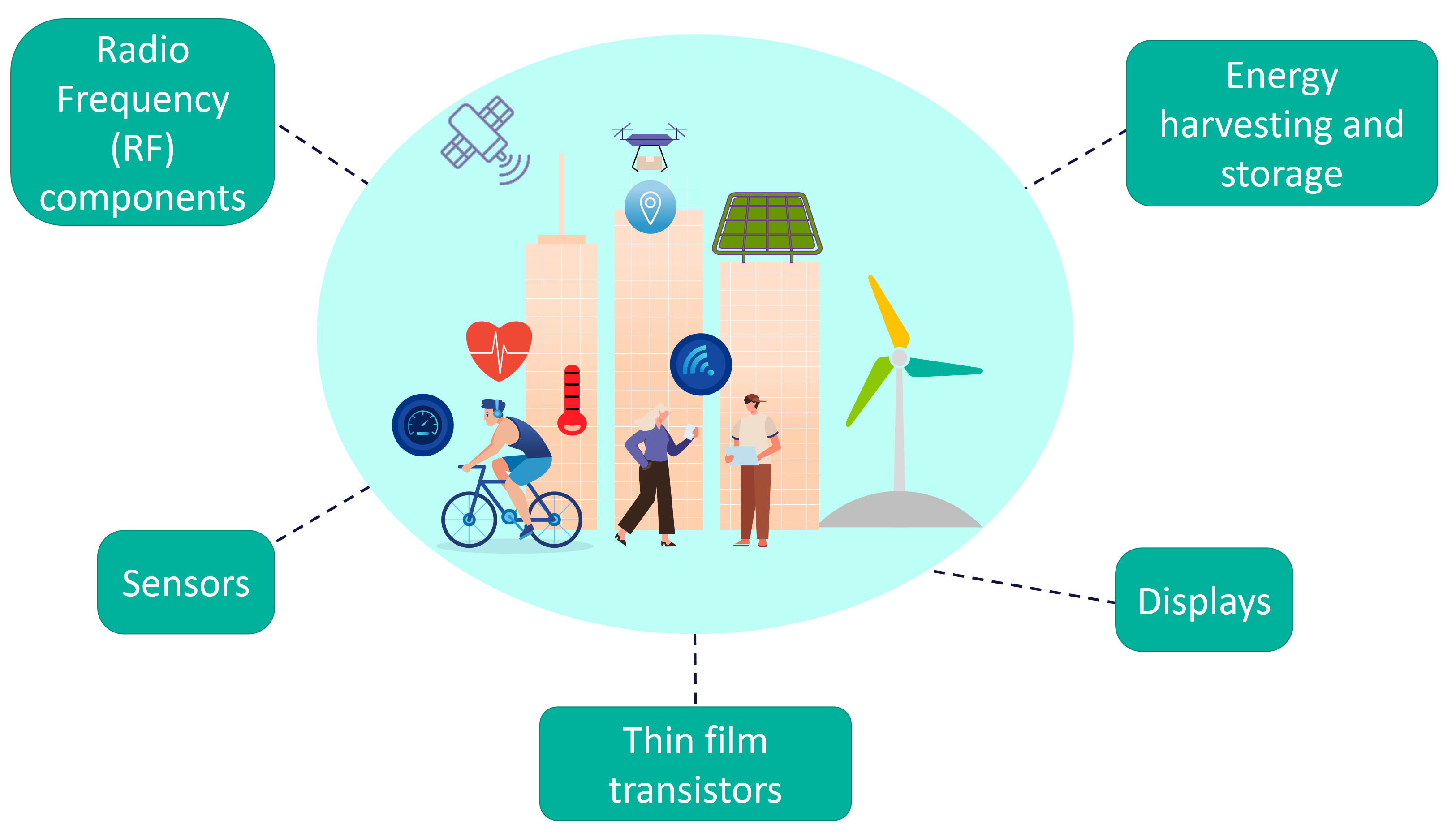
2. Motivation
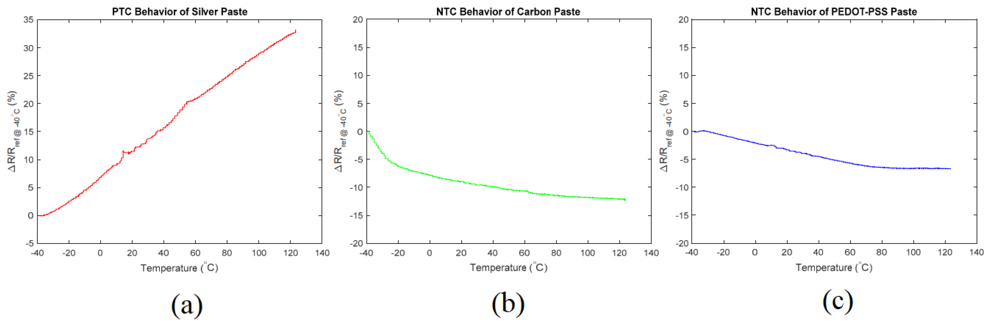
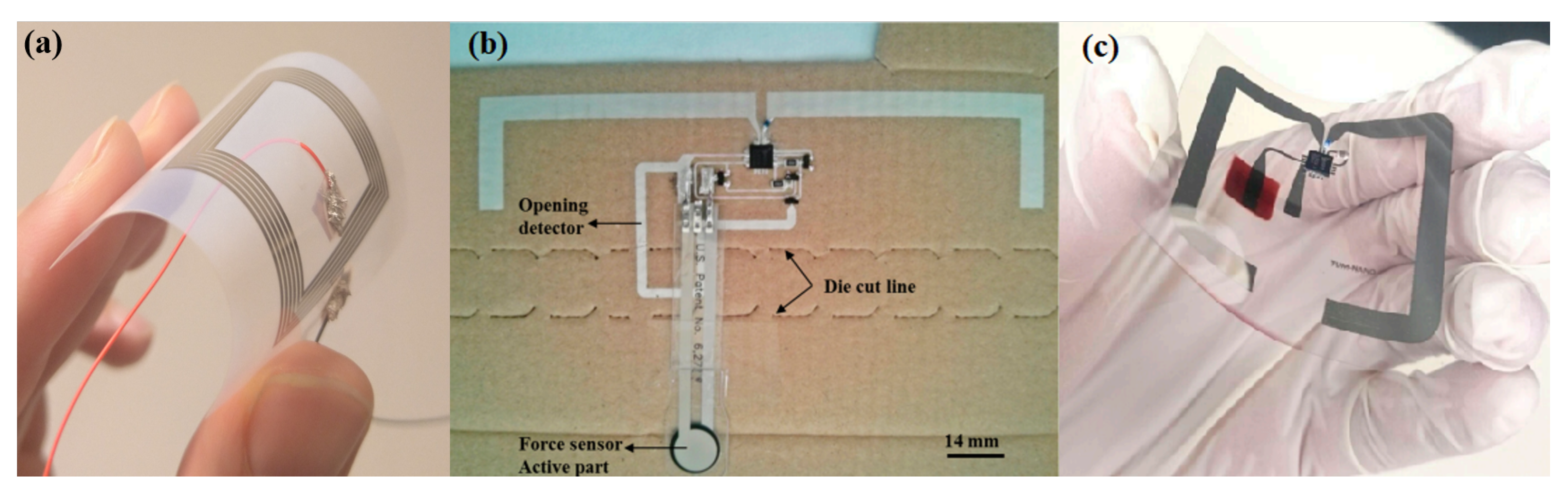
2.1. Sensors
2.2. Thin Film Transistors and Their Applications
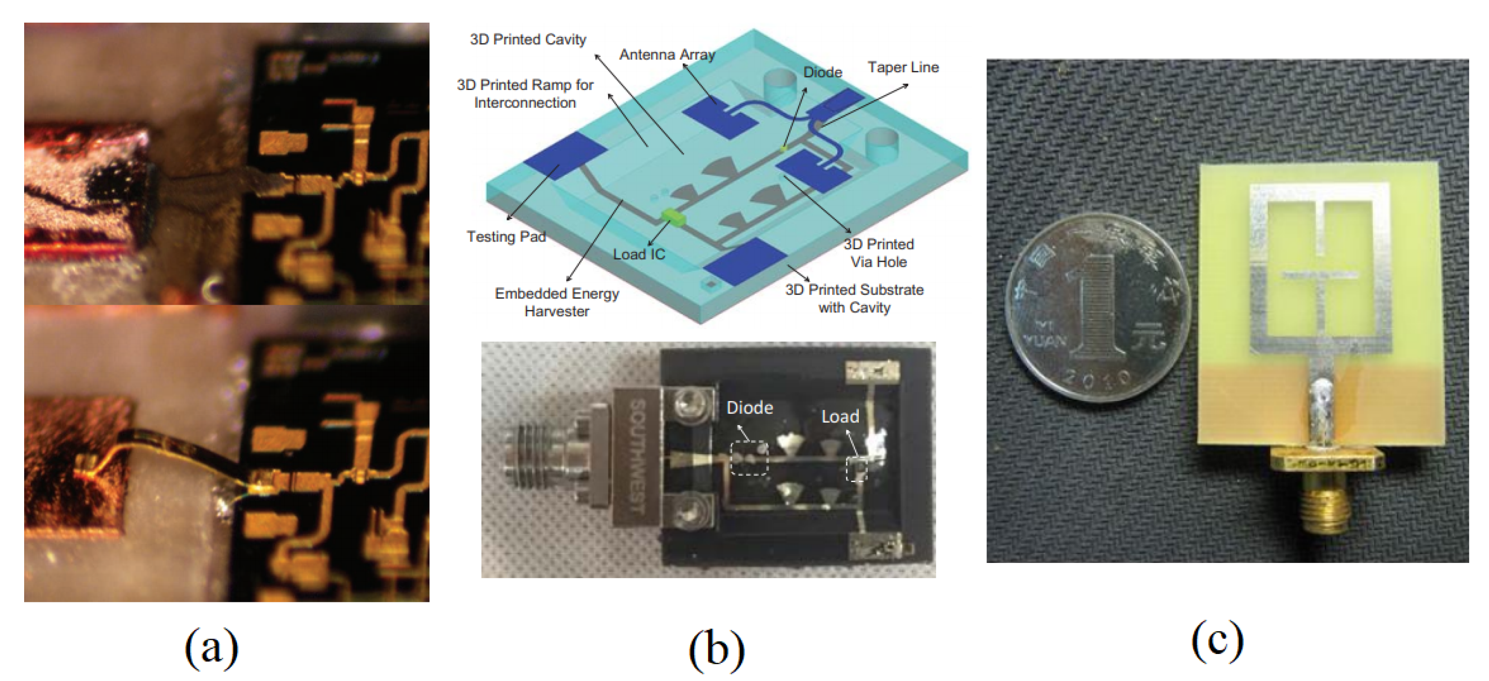
2.3. Radio Frequency (RF) Components
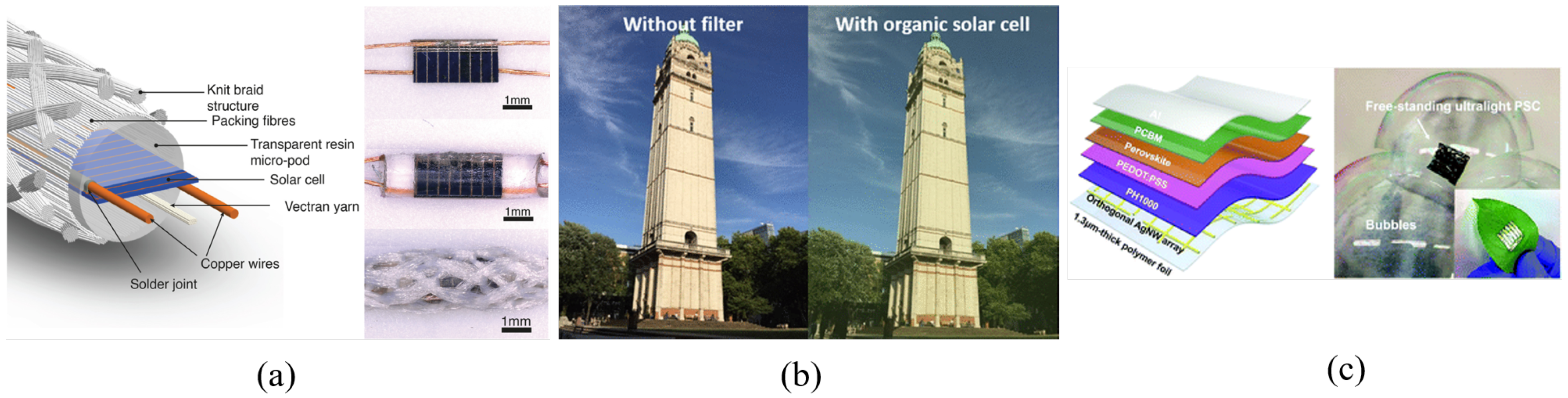
2.4. Energy Harvesting and Storage
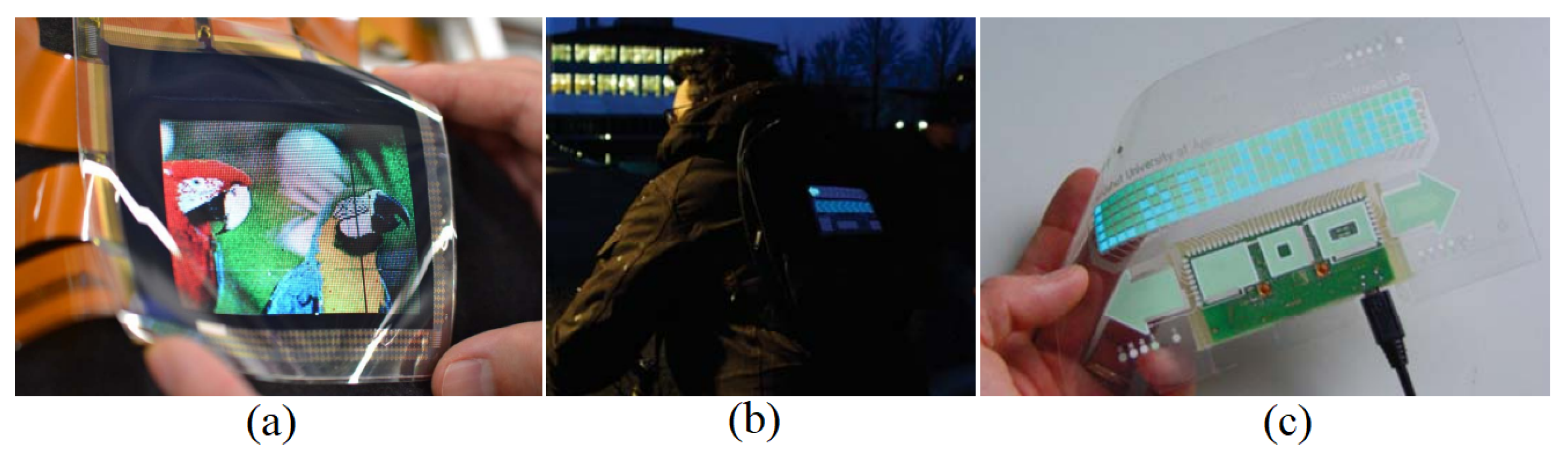
2.5. Displays
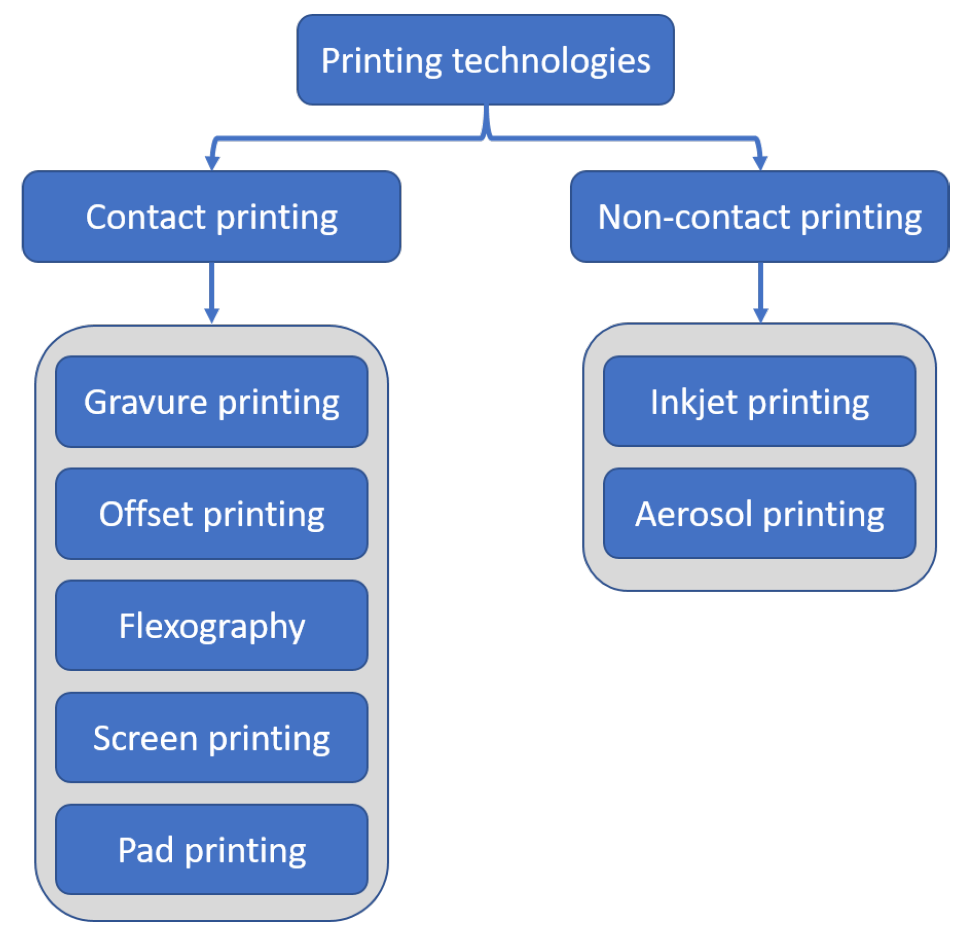
3. Printing Technologies
3.1. Contact Printing Methods with a Master
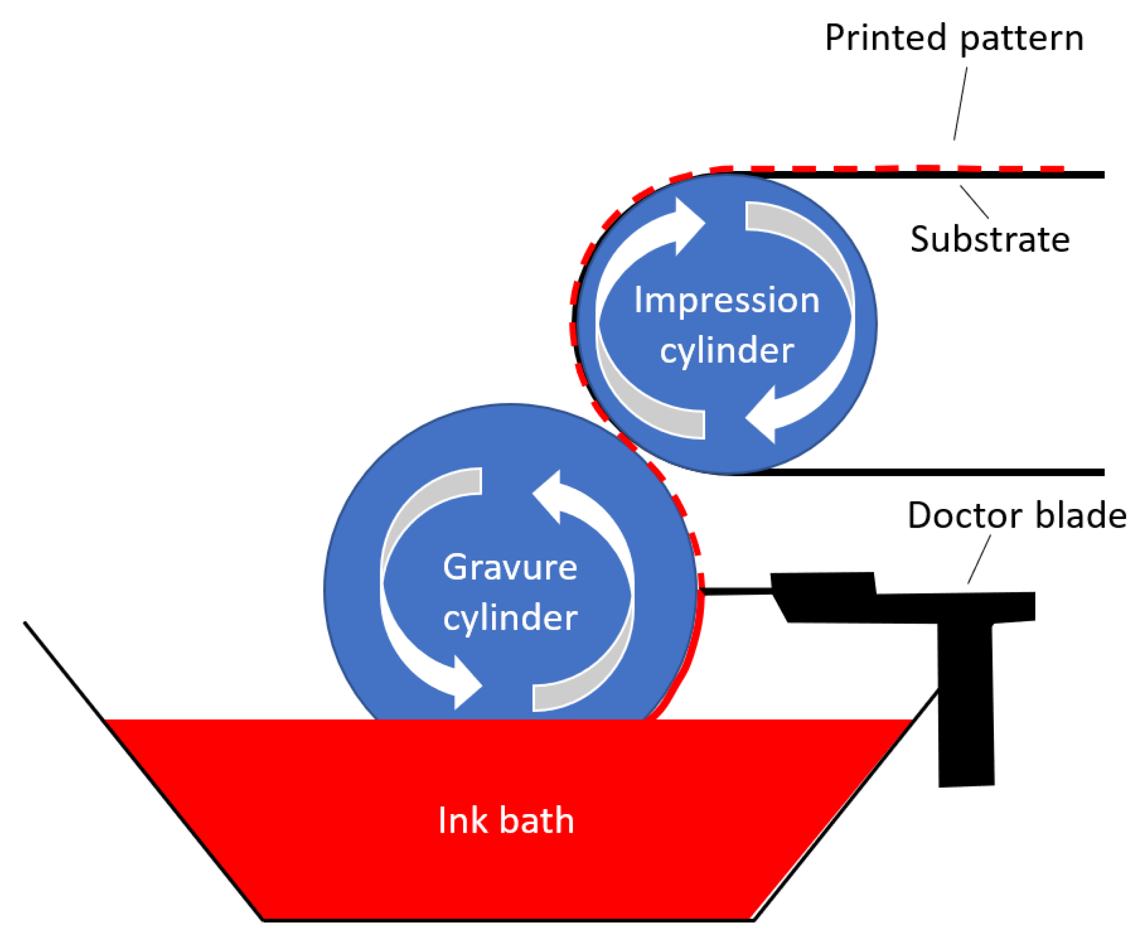
3.1.1. Gravure Printing
3.1.2. Offset Printing
3.1.3. Flexography
3.1.4. Screen Printing
3.1.5. Pad Printing
3.2. Non-Contact Printing Methods
3.2.1. Inkjet Printing
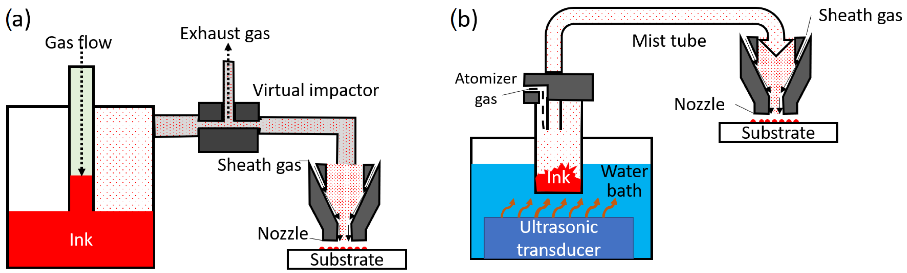
3.2.2. Aerosol Jet Printing
4. Printed Electronic Materials
4.1. Inks for Printed Electronics
4.1.1. Conducting Materials
4.1.2. Semiconducting Materials
4.1.3. Dielectric Materials
4.2. Substrates for Printed Electronics
4.2.1. Natural Polymeric Substrates
4.2.2. Synthetic Polymeric Substrates
5. Characterization of Inks and Substrates
5.1. Ink
5.2. Substrate
5.3. Ink-Substrate Interaction
5.4. Post-Printing Methods for Device Performance
5.5. Life-Cycle Assessment
6. Conclusions
Author Contributions
Funding
Data Availability Statement
Conflicts of Interest
References
- Tan, M.J.; Owh, C.; Chee, P.L.; Kyaw, A.K.K.; Kai, D.; Loh, X.J. Biodegradable electronics: Cornerstone for sustainable electronics and transient applications. J. Mater. Chem. C 2016, 4, 5531–5558. [Google Scholar] [CrossRef]
- Zeng, X.; Yang, C.; Chiang, J.F.; Li, J. Innovating e-waste management: From macroscopic to microscopic scales. Sci. Total. Environ. 2017, 575, 1–5. [Google Scholar] [CrossRef]
- Maddipatla, D.; Narakathu, B.B.; Atashbar, M. Recent Progress in Manufacturing Techniques of Printed and Flexible Sensors: A Review. Biosensors 2020, 12, 199. [Google Scholar] [CrossRef] [PubMed]
- Espera, A.H.; Dizon, J.R.C.; Chen, Q.; Advincula, R.C. 3D-printing and advanced manufacturing for electronics. Prog. Addit. Manuf. 2019, 4, 245–267. [Google Scholar] [CrossRef]
- Gengenbach, U.; Ungerer, M.; Koker, L.; Reichert, K.M.; Stiller, P.; Huang, C.; Hagenmeyer, V. Automated fabrication of multi-layer printed electronic circuits using a novel vector ink-jet printing process control and surface mounting of discrete components. IFAC-PapersOnLine 2019, 52, 609–614. [Google Scholar] [CrossRef]
- Gengenbach, U.; Ungerer, M.; Koker, L.; Reichert, K.M.; Stiller, P.; Allgeier, S.; Köhler, B.; Zhu, X.; Huang, C.; Hagenmeyer, V. Automated fabrication of hybrid printed electronic circuits. Mechatronics 2020, 70, 102403. [Google Scholar] [CrossRef]
- Ostfeld, A.E.; Deckman, I.; Gaikwad, A.M.; Lochner, C.M.; Arias, A.C. Screen printed passive components for flexible power electronics. Sci. Rep. 2015, 5, 15959. [Google Scholar] [CrossRef]
- Ramamoorthy, S.K.; Skrifvars, M.; Persson, A. A review of natural fibers used in biocomposites: Plant, animal and regenerated cellulose fibers. Polym. Rev. 2015, 55, 107–162. [Google Scholar] [CrossRef]
- Kasap, S.; Capper, P. Springer Handbook of Electronic and Photonic Materials; Springer: Berlin/Heidelberg, Germany, 2017. [Google Scholar] [CrossRef] [Green Version]
- Zhang, F.; Saleh, E.; Vaithilingam, J.; Li, Y.; Tuck, C.J.; Hague, R.J.; Wildman, R.D.; He, Y. Reactive material jetting of polyimide insulators for complex circuit board design. Addit. Manuf. 2019, 25, 477–484. [Google Scholar] [CrossRef]
- Beedasy, V.; Smith, P.J. Printed electronics as prepared by inkjet printing. Materials 2020, 13, 704. [Google Scholar] [CrossRef] [Green Version]
- Khan, S.; Lorenzelli, L.; Dahiya, R.S. Technologies for printing sensors and electronics over large flexible substrates: A review. IEEE Sens. J. 2015, 6, 3164–3185. [Google Scholar] [CrossRef]
- Schwartz, D.E.; Rivnay, J.; Whiting, G.L.; Mei, P.; Zhang, Y.; Krusor, B.; Kor, S.; Daniel, G.; Ready, S.E.; Veres, J.; et al. Flexible hybrid electronic circuits and systems. IEEE J. Emerg. Sel. Top. Circuits Syst. 2017, 7, 27–37. [Google Scholar] [CrossRef]
- Chang, J.S.; Facchetti, A.F.; Reuss, R. A Circuits and Systems Perspective of Organic/Printed Electronics: Review, Challenges, and Contemporary and Emerging Design Approaches. IEEE J. Emerg. Sel. Top. Circuits Syst. 2017, 7, 7–26. [Google Scholar] [CrossRef]
- Özkan, M.; Hashmi, S.G.; Halme, J.; Karakoç, A.; Sarikka, T.; Paltakari, J.; Lund, P.D. Inkjet-printed platinum counter electrodes for dye-sensitized solar cells. Org. Electron. 2017, 44, 159–167. [Google Scholar] [CrossRef]
- Sowade, E.; Ramon, E.; Mitra, K.Y.; Martínez-Domingo, C.; Pedró, M.; Pallarès, J.; Loffredo, F.; Villani, F.; Gomes, H.L.; Terés, L.; et al. All-inkjet-printed thin-film transistors: Manufacturing process reliability by root cause analysis. Sci. Rep. 2016, 6, 33490. [Google Scholar] [CrossRef] [PubMed]
- Kjar, A.; Huang, Y. Application of micro-scale 3D printing in pharmaceutics. Pharmaceutics 2019, 11, 390. [Google Scholar] [CrossRef] [PubMed] [Green Version]
- Patil, R.A.; Ramakrishna, S. A comprehensive analysis of e-waste legislation worldwide. Environ. Sci. Pollut. Res. 2020, 27, 14412–14431. [Google Scholar] [CrossRef]
- Higginbotham, S. The internet of trash: IoT has a looming e-waste problem. IEEE Spectr. Technol. Eng. Sci. News 2018, 17. Available online: https://spectrum.ieee.org/the-internet-of-trash-iot-has-a-looming-ewaste-problem (accessed on 30 May 2021).
- Välimäki, M.K.; Sokka, L.I.; Peltola, H.B.; Ihme, S.S.; Rokkonen, T.M.; Kurkela, T.J.; Ollila, J.T.; Korhonen, A.T.; Hast, J.T. Printed and hybrid integrated electronics using bio-based and recycled materials—Increasing sustainability with greener materials and technologies. Int. J. Adv. Manuf. Technol. 2020, 111, 325–339. [Google Scholar] [CrossRef]
- Heacock, M.; Kelly, C.B.; Asante, K.A.; Birnbaum, L.S.; Bergman, Å.L.; Bruné, M.N.; Buka, I.; Carpenter, D.O.; Chen, A.; Huo, X.; et al. E-waste and harm to vulnerable populations: A growing global problem. Environ. Health Perspect. 2016, 124, 550–555. [Google Scholar] [CrossRef] [PubMed]
- Ismail, H.; Hanafiah, M.M. A review of sustainable e-waste generation and management: Present and future perspectives. J. Environ. Manag. 2020, 264, 110495. [Google Scholar] [CrossRef]
- Li, W.; Achal, V. Environmental and health impacts due to e-waste disposal in China—A review. Sci. Total Environ. 2020, 737, 139745. [Google Scholar] [CrossRef]
- Arya, S.; Kumar, S. E-waste in India at a glance: Current trends, regulations, challenges and management strategies. J. Clean. Prod. 2020, 271, 122707. [Google Scholar] [CrossRef]
- Balde, C.; Forti, V.; Gray, V.; Kuehr, R.; Stegmann, P. The Global e-Waste Monitor 2017: Quantities, Flows and Resources; United Nations University: Bonn, Germany; International Telecommunication Union: Geneva, Switzerland; International Solid Waste Association: Vienna, Austria, 2017. [Google Scholar] [CrossRef]
- Joseph, K. Electronic waste management in India–issues and strategies. In Proceedings of the Eleventh International Waste Management and Landfill Symposium, Sardinia, Italy, 1–5 October 2007. [Google Scholar]
- Kunnari, E.; Valkama, J.; Keskinen, M.; Mansikkamäki, P. Environmental evaluation of new technology: Printed electronics case study. J. Clean. Prod. 2009, 9, 791–799. [Google Scholar] [CrossRef]
- Keskinen, M. End-of-life options for printed electronics. In Waste Electrical and Electronic Equipment (WEEE) Handbook; Woodhead Publishing: Sawston, UK, 2012. [Google Scholar] [CrossRef]
- Mraović, M.; Muck, T.; Pivar, M.; Trontelj, J.; Pleteršek, A. Humidity sensors printed on recycled paper and cardboard. Sensors 2014, 14, 13628–13643. [Google Scholar] [CrossRef] [PubMed] [Green Version]
- Tuukkanen, S.; Välimäki, M.; Lehtimäki, S.; Vuorinen, T.; Lupo, D. Behaviour of one-step spray-coated carbon nanotube supercapacitor in ambient light harvester circuit with printed organic solar cell and electrochromic display. Sci. Rep. 2016, 6, 22967. [Google Scholar] [CrossRef] [PubMed]
- Ostfeld, A.E.; Arias, A.C. Flexible photovoltaic power systems: Integration opportunities, challenges and advances. Flex. Print. Electron. 2017, 2, 013001. [Google Scholar] [CrossRef] [Green Version]
- Ataeefard, M.; Khamseh, S. Design of conductive pattern on recycled paper. Pigment Resin Technol. 2019, 48, 409–414. [Google Scholar] [CrossRef]
- Pickard, W.F. Geochemical constraints on sustainable development: Can an advanced global economy achieve long-term stability? Glob. Planet. Chang. 2008, 61, 285–299. [Google Scholar] [CrossRef]
- Aliaga, C.; Ferreira, B.; Hortal, M.; Pancorbo, M.Á.; López, J.M.; Navas, F.J. Influence of RFID tags on recyclability of plastic packaging. Waste Manag. 2011, 31, 1133–1138. [Google Scholar] [CrossRef]
- Lehtimaäki, S.; Suominen, M.; Damlin, P.; Tuukkanen, S.; Kvarnstroöm, C.; Lupo, D. Preparation of supercapacitors on flexible substrates with electrodeposited PEDOT/graphene composites. ACS Appl. Mater. Interfaces 2015, 7, 22137–22147. [Google Scholar] [CrossRef]
- Cheng, I.C.; Wagner, S. Overview of flexible electronics technology. In Flexible Electronics; Springer: Berlin/Heidelberg, Germany, 2009; pp. 1–28. [Google Scholar]
- Nathan, A.; Ahnood, A.; Cole, M.T.; Lee, S.; Suzuki, Y.; Hiralal, P.; Bonaccorso, F.; Hasan, T.; Garcia-Gancedo, L.; Dyadyusha, A.; et al. Flexible electronics: The next ubiquitous platform. Proc. IEEE 2012, 100, 1486–1517. [Google Scholar] [CrossRef]
- Salmerón, J.F.; Molina-Lopez, F.; Briand, D.; Ruan, J.J.; Rivadeneyra, A.; Carvajal, M.A.; Capitán-Vallvey, L.F.; de Rooij, N.F.; Palma, A.J. Properties and Printability of Inkjet and Screen-Printed Silver Patterns for RFID Antennas. J. Electron. Mater. 2014, 43, 604–617. [Google Scholar] [CrossRef]
- Fernández-Salmerón, J.; Rivadeneyra, A.; Martínez-Martí, F.; Capitán-Vallvey, L.F.; Palma, A.J.; Carvajal, M.A. Passive UHF RFID tag with multiple sensing capabilities. Sensors 2015, 15, 26769–26782. [Google Scholar] [CrossRef] [Green Version]
- Falco, A.; Salmerón, J.F.; Loghin, F.C.; Lugli, P.; Rivadeneyra, A. Fully Printed Flexible Single-Chip RFID Tag with Light Detection Capabilities. Sensors 2017, 17, 534. [Google Scholar] [CrossRef]
- Berggren, M.; Nilsson, D.; Robinson, N.D. Organic materials for printed electronics. Nat. Mater. 2007, 6, 3–5. [Google Scholar] [CrossRef] [PubMed]
- Kamyshny, A.; Magdassi, S. Conductive nanomaterials for printed electronics. Small 2014, 10, 3515–3535. [Google Scholar] [CrossRef] [PubMed]
- Khan, Y.; Thielens, A.; Muin, S.; Ting, J.; Baumbauer, C.; Arias, A.C. A new frontier of printed electronics: Flexible hybrid electronics. Adv. Mater. 2020, 32, 1905279. [Google Scholar] [CrossRef] [PubMed]
- Perelaer, J.; Smith, P.J.; Mager, D.; Soltman, D.; Volkman, S.K.; Subramanian, V.; Korvink, J.G.; Schubert, U.S. Printed electronics: The challenges involved in printing devices, interconnects, and contacts based on inorganic materials. J. Mater. Chem. 2010, 20, 8446–8453. [Google Scholar] [CrossRef]
- Clemens, W.; Fix, W.; Ficker, J.; Knobloch, A.; Ullmann, A. From polymer transistors toward printed electronics. J. Mater. Res. 2004, 19, 1963–1973. [Google Scholar] [CrossRef]
- Tomotoshi, D.; Kawasaki, H. Surface and interface designs in copper-based conductive inks for printed/flexible electronics. Nanomaterials 2020, 10, 1689. [Google Scholar] [CrossRef] [PubMed]
- Mackanic, D.G.; Chang, T.H.; Huang, Z.; Cui, Y.; Bao, Z. Stretchable electrochemical energy storage devices. Chem. Soc. Rev. 2020, 49, 4466–4495. [Google Scholar] [CrossRef] [PubMed]
- Popov, V.I.; Kotin, I.A.; Nebogatikova, N.A.; Smagulova, S.A.; Antonova, I.V. Graphene-PEDOT: PSS Humidity Sensors for High Sensitive, Low-Cost, Highly-Reliable, Flexible, and Printed Electronics. Materials 2019, 12, 3477. [Google Scholar] [CrossRef] [Green Version]
- Rivadeneyra, A.; Bobinger, M.; Albrecht, A.; Becherer, M.; Lugli, P.; Falco, A.; Salmerón, J.F. Cost-effective PEDOT:PSS Temperature Sensors Inkjetted on a Bendable Substrate by a Consumer Printer. Polymers 2019, 11, 824. [Google Scholar] [CrossRef] [PubMed] [Green Version]
- Lall, P.; Goyal, K.; Narangaparambil, J. Accuracy, Hysteresis and Extended Time Stability of Additively Printed Temperature and Humidity Sensors. In Proceedings of the 2020 IEEE 70th Electronic Components and Technology Conference (ECTC), Orlando, FL, USA, 3–30 June 2020. [Google Scholar] [CrossRef]
- Kim, T.; Bao, C.; Hausmann, M.; Siqueira, G.; Zimmermann, T.; Kim, W.S. 3D printed disposable wireless ion sensors with biocompatible cellulose composites. Adv. Electron. Mater. 2019, 5, 1800778. [Google Scholar] [CrossRef]
- Ling, H.; Chen, R.; Huang, Q.; Shen, F.; Wang, Y.; Wang, X. Transparent, flexible and recyclable nanopaper-based touch sensors fabricated via inkjet-printing. Green Chem. 2020, 22, 3208–3215. [Google Scholar] [CrossRef]
- Guo, Y.; Chen, S.; Sun, L.; Yang, L.; Zhang, L.; Lou, J.; You, Z. Degradable and Fully Recyclable Dynamic Thermoset Elastomer for 3D-Printed Wearable Electronics. Adv. Funct. Mater. 2021, 31, 2009799. [Google Scholar] [CrossRef]
- Hsiao, F.R.; Liao, Y.C. Printed Micro-Sensors for Simultaneous Temperature and Humidity Detection. IEEE Sens. J. 2018, 18, 6788–6793. [Google Scholar] [CrossRef]
- Sui, Y.; Kreider, L.P.; Bogie, K.M.; Zorman, C.A. Fabrication of a Silver-Based Thermistor on Flexible, Temperature-Sensitive Substrates Using a Low-Temperature Inkjet Printing Technique. IEEE Sens. Lett. 2019, 3, 1–4. [Google Scholar] [CrossRef]
- Sappati, K.K.; Bhadra, S. Printed Polymer based Acoustic Sensor for Temperature Monitoring. In Proceedings of the 2020 IEEE International Conference on Flexible and Printable Sensors and Systems (FLEPS), Manchester, UK, 16–19 August 2020; pp. 1–4. [Google Scholar] [CrossRef]
- Gieva, E.E.; Nikolov, G.T.; Nikolova, B.M.; Ruskova, I.N. Temperature Sensing with Inkjet Printed Structures. In Proceedings of the 2019 IEEE XXVIII International Scientific Conference Electronics (ET), Sozopol, Bulgaria, 12–14 September 2019; pp. 1–4. [Google Scholar] [CrossRef]
- Kuzubasoglu, B.A.; Sayar, E.; Bahadir, S.K. Inkjet-printed CNT/PEDOT:PSS temperature sensor on a textile substrate for wearable intelligent systems. IEEE Sens. J. 2021. [Google Scholar] [CrossRef]
- Lin, S.C.; Liao, Y.C. Integrated humidity and temperature sensing circuit fabricated by inkjet printing technology. In Proceedings of the 2016 11th International Microsystems, Packaging, Assembly and Circuits Technology Conference (IMPACT), Taipei, Taiwan, 26–28 October 2016; pp. 59–61. [Google Scholar] [CrossRef]
- Morales-Rodríguez, M.E.; Joshi, P.C.; Humphries, J.R.; Fuhr, P.L.; Mcintyre, T.J. Fabrication of Low Cost Surface Acoustic Wave Sensors Using Direct Printing by Aerosol Inkjet. IEEE Access 2018, 6, 20907–20915. [Google Scholar] [CrossRef]
- Vuorinen, T.; Niittynen, J.; Kankkunen, T.; Kraft, T.M.; Mäntysalo, M. Inkjet-printed graphene/PEDOT: PSS temperature sensors on a skin-conformable polyurethane substrate. Sci. Rep. 2016, 6, 35289. [Google Scholar] [CrossRef]
- Siddique, S.; Park, J.G.; Andrei, P.; Liang, R. M3D aerosol jet printed buckypaper multifunctional sensors for composite structural health monitoring. Results Phys. 2019. [Google Scholar] [CrossRef]
- Wang, Y.F.; Sekine, T.; Takeda, Y.; Hong, J.; Yoshida, A.; Matsui, H.; Kumaki, D.; Nishikawa, T.; Shiba, T.; Sunaga, T.; et al. Printed Strain Sensor with High Sensitivity and Wide Working Range Using a Novel Brittle–Stretchable Conductive Network. ACS Appl. Mater. Interfaces 2020, 12, 35282–35290. [Google Scholar] [CrossRef]
- Li, S.; Kosek, A.; Jahangir, M.N.; Malhotra, R.; Chang, C.H. Inkjet Printing of Perovskites for Breaking Performance–Temperature Tradeoffs in Fabric-Based Thermistors. Adv. Funct. Mater. 2021, 31, 2006273. [Google Scholar] [CrossRef]
- Zymelka, D.; Togashi, K.; Ohigashi, R.; Yamashita, T.; Takamatsu, S.; Itoh, T.; Kobayashi, T. Printed strain sensor array for application to structural health monitoring. Smart Mater. Struct. 2017, 26, 105040. [Google Scholar] [CrossRef]
- Lee, G.Y.; Kim, M.S.; Yoon, H.S.; Yang, J.; Ihn, J.B.; Ahn, S.H. Direct printing of strain sensors via nanoparticle printer for the applications to composite structural health monitoring. Procedia CIRP 2017, 66, 238–242. [Google Scholar] [CrossRef]
- Demuru, S.; Marette, A.; Kooli, W.; Junier, P.; Briand, D. Flexible Organic Electrochemical Transistor with Functionalized Inkjet-Printed Gold Gate for Bacteria Sensing. In Proceedings of the 2019 20th International Conference on Solid-State Sensors, Actuators and Microsystems Eurosensors XXXIII (Transducers Eurosensors XXXIII), Berlin, Germany, 23–27 June 2019; pp. 2519–2522. [Google Scholar] [CrossRef]
- Laurila, M.M.; Matsui, H.; Shiwaku, R.; Peltokangas, M.; Verho, J.; Montero, K.L.; Sekine, T.; Vehkaoja, A.; Oksala, N.; Tokito, S.; et al. A Fully Printed Ultra-Thin Charge Amplifier for On-Skin Biosignal Measurements. IEEE J. Electron Devices Soc. 2019, 7, 566–574. [Google Scholar] [CrossRef]
- Portilla, L.; Zhao, J.; Wang, Y.; Sun, L.; Li, F.; Robin, M.; Wei, M.; Cui, Z.; Occhipinti, L.G.; Anthopoulos, T.D.; et al. Ambipolar Deep-Subthreshold Printed-Carbon-Nanotube Transistors for Ultralow-Voltage and Ultralow-Power Electronics. ACS Nano 2020, 14, 14036–14046. [Google Scholar] [CrossRef]
- Williams, N.X.; Bullard, G.; Brooke, N.; Therien, M.J.; Franklin, A.D. Fully printed, all-carbon, recyclable electronics. arXiv 2020, arXiv:2009.10225. [Google Scholar]
- Williams, N.X.; Bullard, G.; Brooke, N.; Therien, M.J.; Franklin, A.D. Printable and recyclable carbon electronics using crystalline nanocellulose dielectrics. Nat. Electron. 2021, 4, 261–268. [Google Scholar] [CrossRef]
- Matsui, H.; Hayasaka, K.; Takeda, Y.; Shiwaku, R.; Kwon, J.; Tokito, S. Printed 5-V organic operational amplifiers for various signal processing. Sci. Rep. 2018, 8, 8980. [Google Scholar] [CrossRef]
- Sun, H.; Xu, Y.; Noh, Y.Y. Flexible Organic Amplifiers. IEEE Trans. Electron Devices 2017, 64, 1944–1954. [Google Scholar] [CrossRef]
- Weller, D.; Cadilha Marques, G.; Aghassi-Hagmann, J.; Tahoori, M.B. An Inkjet-Printed Low-Voltage Latch Based on Inorganic Electrolyte-Gated Transistors. IEEE Electron Device Lett. 2018, 39, 831–834. [Google Scholar] [CrossRef]
- Kamali-Sarvestani, R.; Martin, B.; Brayden, L. Design and Fabrication of Ink-Jet Printed Logic Gates using SWCNT-FET for Flexible Circuit Applications. In Proceedings of the 2019 IEEE International Symposium on Circuits and Systems (ISCAS), Sapporo, Japan, 26–29 May 2019; pp. 1–5. [Google Scholar] [CrossRef]
- Singh, S.; Takeda, Y.; Matsui, H.; Tokito, S. Flexible PMOS Inverter and NOR Gate Using Inkjet-Printed Dual-Gate Organic Thin Film Transistors. IEEE Electron Device Lett. 2020, 41, 409–412. [Google Scholar] [CrossRef]
- Kheradmand-Boroujeni, B.; Schmidt, G.C.; Höft, D.; Bellmann, M.; Haase, K.; Ishida, K.; Shabanpour, R.; Meister, T.; Carta, C.; Ghesquiere, P.; et al. A Fully-Printed Self-Biased Polymeric Audio Amplifier for Driving Fully-Printed Piezoelectric Loudspeakers. IEEE Trans. Circuits Syst. I Regul. Pap. 2016, 63, 785–794. [Google Scholar] [CrossRef]
- Want, R. An introduction to RFID technology. IEEE Pervasive Comput. 2006, 5, 25–33. [Google Scholar] [CrossRef]
- Nasri, N.; Kachouri, N.; Samet, M.; Andrieux, L. Radio Frequency IDentification (RFID) working, design considerations and modelling of antenna. In Proceedings of the 2008 5th International Multi-Conference on Systems, Signals and Devices, Amman, Jordan, 20–22 July 2008. [Google Scholar] [CrossRef]
- Weinstein, R. RFID: A technical overview and its application to the enterprise. IT Prof. 2005, 7, 27–33. [Google Scholar] [CrossRef]
- Voigt, M.M.; Guite, A.; Chung, D.Y.; Khan, R.U.A.; Campbell, A.J.; Bradley, D.D.C.; Meng, F.; Steinke, J.H.G.; Tierney, S.; McCulloch, I.; et al. Polymer Field-Effect Transistors Fabricated by the Sequential Gravure Printing of Polythiophene, Two Insulator Layers, and a Metal Ink Gate. Adv. Funct. Mater. 2010, 20, 239–246. [Google Scholar] [CrossRef]
- Xiao, G.; Zhang, Z.; Fukutani, H.; Tao, Y.; Lang, S. Improving the Q -Factor of Printed HF RFID Loop Antennas on Flexible Substrates by Condensing the Microstructures of Conductors. IEEE J. Radio Freq. Identif. 2018. [Google Scholar] [CrossRef]
- Eid, A.; He, X.; Bahr, R.; Lin, T.H.; Cui, Y.; Adeyeye, A.; Tehrani, B.; Tentzeris, M.M. Inkjet-/3D-/4D-Printed Perpetual Electronics and Modules: RF and mm-Wave Devices for 5G+, IoT, Smart Agriculture, and Smart Cities Applications. IEEE Microw. Mag. 2020. [Google Scholar] [CrossRef]
- Wang, Y.; Chen, C.L. A Triple-Band Printed Monopole Antenna for WLAN/WiMAX/5G Applications. In Proceedings of the 2020 IEEE 3rd International Conference on Electronic Information and Communication Technology (ICEICT), Shenzhen, China, 13–15 November 2020. [Google Scholar] [CrossRef]
- Jilani, S.; Alomainy, A. An inkjet-printed MMW frequency-reconfigurable antenna on a flexible PET substrate for 5G wireless systems. In Proceedings of the Loughborough Antennas & Propagation Conference (LAPC 2017), Loughborough, UK, 13–14 November 2017. [Google Scholar] [CrossRef]
- Lin, T.H.; Daskalakis, S.N.; Georgiadis, A.; Tentzeris, M.M. Achieving Fully Autonomous System-on-Package Designs: An Embedded-on-Package 5G Energy Harvester within 3D Printed Multilayer Flexible Packaging Structures. In Proceedings of the 2019 IEEE MTT-S International Microwave Symposium (IMS), Boston, MA, USA, 2–7 June 2019. [Google Scholar] [CrossRef]
- Sundriyal, P.; Bhattacharya, S. Inkjet-printed electrodes on A4 paper substrates for low-cost, disposable, and flexible asymmetric supercapacitors. ACS Appl. Mater. Interfaces 2017, 9, 38507–38521. [Google Scholar] [CrossRef]
- Choi, Y.M.; Lee, M.G.; Jeon, Y. Wearable biomechanical energy harvesting technologies. Energies 2017, 10, 1483. [Google Scholar] [CrossRef] [Green Version]
- Pacchierotti, C.; Sinclair, S.; Solazzi, M.; Frisoli, A.; Hayward, V.; Prattichizzo, D. Wearable haptic systems for the fingertip and the hand: Taxonomy, review, and perspectives. IEEE Trans. Haptics 2017, 10, 580–600. [Google Scholar] [CrossRef] [PubMed] [Green Version]
- Javed, M.S.; Zhong, D.; Ma, T.; Song, A.; Ahmed, S. Hybrid pumped hydro and battery storage for renewable energy based power supply system. Appl. Energy 2020, 257, 114026. [Google Scholar] [CrossRef]
- Wang, C.; Xia, K.; Wang, H.; Liang, X.; Yin, Z.; Zhang, Y. Advanced carbon for flexible and wearable electronics. Adv. Mater. 2019, 31, 1801072. [Google Scholar] [CrossRef] [PubMed]
- Qin, J.; Lan, L.; Chen, S.; Huang, F.; Shi, H.; Chen, W.; Xia, H.; Sun, K.; Yang, C. Recent progress in flexible and stretchable organic solar cells. Adv. Funct. Mater. 2020, 30, 2002529. [Google Scholar] [CrossRef]
- Lee, J.; Cha, H.; Yao, H.; Hou, J.; Suh, Y.H.; Jeong, S.; Lee, K.; Durrant, J.R. Toward Visibly Transparent Organic Photovoltaic Cells Based on a Near-Infrared Harvesting Bulk Heterojunction Blend. ACS Appl. Mater. Interfaces 2020, 12, 32764–32770. [Google Scholar] [CrossRef] [PubMed]
- Kang, S.; Jeong, J.; Cho, S.; Yoon, Y.J.; Park, S.; Lim, S.; Kim, J.Y.; Ko, H. Ultrathin lightweight and flexible perovskite solar cells with an excellent power-per-weight performance. J. Mater. Chem. A 2019, 7, 1107–1114. [Google Scholar] [CrossRef]
- Shepelin, N.A.; Lussini, V.C.; Fox, P.J.; Dicinoski, G.W.; Glushenkov, A.M.; Shapter, J.G.; Ellis, A.V. 3D printing of poly (vinylidene fluoride-trifluoroethylene): A poling-free technique to manufacture flexible and transparent piezoelectric generators. MRS Commun. 2019, 9, 159–164. [Google Scholar] [CrossRef]
- Shepelin, N.A.; Sherrell, P.C.; Goudeli, E.; Skountzos, E.N.; Lussini, V.C.; Dicinoski, G.W.; Shapter, J.G.; Ellis, A.V. Printed recyclable and self-poled polymer piezoelectric generators through single-walled carbon nanotube templating. Energy Environ. Sci. 2020, 13, 868–883. [Google Scholar] [CrossRef]
- Satharasinghe, A.; Hughes-Riley, T.; Dias, T. An investigation of a wash-durable solar energy harvesting textile. Prog. Photovolt. Res. Appl. 2020, 28, 578–592. [Google Scholar] [CrossRef]
- Baran, D.; Corzo, D.; Blazquez, G.T. Flexible Electronics: Status, Challenges and Opportunities. Front. Electron. 2020, 1, 2. [Google Scholar]
- Battaglia, C.; Cuevas, A.; De Wolf, S. High-efficiency crystalline silicon solar cells: Status and perspectives. Energy Environ. Sci. 2016, 9, 1552–1576. [Google Scholar] [CrossRef] [Green Version]
- Masuko, K.; Shigematsu, M.; Hashiguchi, T.; Fujishima, D.; Kai, M.; Yoshimura, N.; Yamaguchi, T.; Ichihashi, Y.; Mishima, T.; Matsubara, N.; et al. Achievement of more than 25% conversion efficiency with crystalline silicon heterojunction solar cell. IEEE J. Photovolt. 2014, 4, 1433–1435. [Google Scholar] [CrossRef]
- Feldmann, F.; Simon, M.; Bivour, M.; Reichel, C.; Hermle, M.; Glunz, S. Carrier-selective contacts for Si solar cells. Appl. Phys. Lett. 2014, 104, 181105. [Google Scholar] [CrossRef]
- Riede, M.; Spoltore, D.; Leo, K. Organic Solar Cells—The Path to Commercial Success. Adv. Energy Mater. 2021, 11, 2002653. [Google Scholar] [CrossRef]
- Ahlswede, E.; Mühleisen, W.; bin Moh Wahi, M.W.; Hanisch, J.; Powalla, M. Highly efficient organic solar cells with printable low-cost transparent contacts. Appl. Phys. Lett. 2008, 92, 127. [Google Scholar] [CrossRef]
- Vogelbaum, H.S.; Sauvé, G. Recently developed high-efficiency organic photoactive materials for printable photovoltaic cells: A mini review. Synth. Met. 2017, 223, 107–121. [Google Scholar] [CrossRef] [Green Version]
- Li, Y.; Xu, G.; Cui, C.; Li, Y. Flexible and semitransparent organic solar cells. Adv. Energy Mater. 2018, 8, 1701791. [Google Scholar] [CrossRef]
- Facchetti, A. π-Conjugated polymers for organic electronics and photovoltaic cell applications. Chem. Mater. 2011, 23, 733–758. [Google Scholar] [CrossRef]
- Eggenhuisen, T.; Galagan, Y.; Biezemans, A.; Slaats, T.; Voorthuijzen, P.; Kommeren, S.; Shanmugam, S.; Teunissen, P.; Hadipour, A.; Verhees, W.; et al. High efficiency, fully inkjet printed organic solar cells with freedom of design. J. Mater. Chem. A 2015, 3. [Google Scholar] [CrossRef] [Green Version]
- Cheng, P.; Zhan, X. Stability of organic solar cells: Challenges and strategies. Chem. Soc. Rev. 2016, 45, 2544–2582. [Google Scholar] [CrossRef]
- Zhao, J.; Li, Y.; Yang, G.; Jiang, K.; Lin, H.; Ade, H.; Ma, W.; Yan, H. Efficient organic solar cells processed from hydrocarbon solvents. Nat. Energy 2016, 1, 1–7. [Google Scholar] [CrossRef]
- Hu, Z.; Wang, J.; Ma, X.; Gao, J.; Xu, C.; Wang, X.; Zhang, X.; Wang, Z.; Zhang, F. Semitransparent organic solar cells exhibiting 13.02% efficiency and 20.2% average visible transmittance. J. Mater. Chem. A 2021, 9, 6797–6804. [Google Scholar] [CrossRef]
- Kim, Y.; Lim, E. Development of polymer acceptors for organic photovoltaic cells. Polymers 2014, 6, 382–407. [Google Scholar] [CrossRef]
- Liu, S.; Chen, D.; Hu, X.; Xing, Z.; Wan, J.; Zhang, L.; Tan, L.; Zhou, W.; Chen, Y. Printable and Large-Area Organic Solar Cells Enabled by a Ternary Pseudo-Planar Heterojunction Strategy. Adv. Funct. Mater. 2020, 30, 2003223. [Google Scholar] [CrossRef]
- Yoo, J.J.; Seo, G.; Chua, M.R.; Park, T.G.; Lu, Y.; Rotermund, F.; Kim, Y.K.; Moon, C.S.; Jeon, N.J.; Correa-Baena, J.P.; et al. Efficient perovskite solar cells via improved carrier management. Nature 2021, 590, 587–593. [Google Scholar] [CrossRef] [PubMed]
- Pendyala, N.K.; Magdassi, S.; Etgar, L. Fabrication of Perovskite Solar Cells with Digital Control of Transparency by Inkjet Printing. ACS Appl. Mater. Interfaces 2021. [Google Scholar] [CrossRef]
- Zhang, L.; Chen, S.; Wang, X.; Wang, D.; Li, Y.; Ai, Q.; Sun, X.; Chen, J.; Li, Y.; Jiang, X.; et al. ambient inkjet-printed high-efficiency perovskite solar cells: Manipulating the spreading and crystallization behaviors of picoliter perovskite droplets. Sol. RRL 2021, 5, 2100106. [Google Scholar] [CrossRef]
- Schackmar, F.; Eggers, H.; Frericks, M.; Richards, B.S.; Lemmer, U.; Hernandez-Sosa, G.; Paetzold, U.W. Perovskite Solar Cells with All-Inkjet-Printed Absorber and Charge Transport Layers. Adv. Mater. Technol. 2021, 6, 2000271. [Google Scholar] [CrossRef]
- Li, P.; Liang, C.; Bao, B.; Li, Y.; Hu, X.; Wang, Y.; Zhang, Y.; Li, F.; Shao, G.; Song, Y. Inkjet manipulated homogeneous large size perovskite grains for efficient and large-area perovskite solar cells. Nano Energy 2018, 46, 203–211. [Google Scholar] [CrossRef]
- Eggers, H.; Schackmar, F.; Abzieher, T.; Sun, Q.; Lemmer, U.; Vaynzof, Y.; Richards, B.S.; Hernandez-Sosa, G.; Paetzold, U.W. Inkjet-Printed Micrometer-Thick Perovskite Solar Cells with Large Columnar Grains. Adv. Energy Mater. 2020, 10, 1903184. [Google Scholar] [CrossRef] [Green Version]
- Li, Z.; Li, P.; Chen, G.; Cheng, Y.; Pi, X.; Yu, X.; Yang, D.; Han, L.; Zhang, Y.; Song, Y. Ink engineering of inkjet printing perovskite. ACS Appl. Mater. Interfaces 2020, 12, 39082–39091. [Google Scholar] [CrossRef]
- Liu, S.; Yuan, J.; Deng, W.; Luo, M.; Xie, Y.; Liang, Q.; Zou, Y.; He, Z.; Wu, H.; Cao, Y. High-efficiency organic solar cells with low non-radiative recombination loss and low energetic disorder. Nat. Photonics 2020, 14, 300–305. [Google Scholar] [CrossRef]
- Ma, R.; Tao, Y.; Chen, Y.; Liu, T.; Luo, Z.; Guo, Y.; Xiao, Y.; Fang, J.; Zhang, G.; Li, X.; et al. Achieving 16.68% efficiency ternary as-cast organic solar cells. Sci. China Chem. 2021, 64, 581–589. [Google Scholar] [CrossRef]
- Cai, Y.; Li, Y.; Wang, R.; Wu, H.; Chen, Z.; Zhang, J.; Ma, Z.; Hao, X.; Zhao, Y.; Zhang, C.; et al. A Well-Mixed Phase Formed by Two Compatible Non-Fullerene Acceptors Enables Ternary Organic Solar Cells with Efficiency over 18.6%. Adv. Mater. 2021, 2101733. [Google Scholar] [CrossRef]
- Hu, L.; Wu, H.; Cui, Y. Printed energy storage devices by integration of electrodes and separators into single sheets of paper. Appl. Phys. Lett. 2010, 96, 183502. [Google Scholar] [CrossRef]
- Brunetti, F.; Operamolla, A.; Castro-Hermosa, S.; Lucarelli, G.; Manca, V.; Farinola, G.M.; Brown, T.M. Printed solar cells and energy storage devices on paper substrates. Adv. Funct. Mater. 2019, 29, 1806798. [Google Scholar] [CrossRef] [Green Version]
- Zhang, W.; Liu, H.; Zhang, X.; Li, X.; Zhang, G.; Cao, P. 3D Printed Micro-Electrochemical Energy Storage Devices: From Design to Integration. Adv. Funct. Mater. 2021, 2104909. [Google Scholar] [CrossRef]
- Xing, J.; Tao, P.; Wu, Z.; Xing, C.; Liao, X.; Nie, S. Nanocellulose-graphene composites: A promising nanomaterial for flexible supercapacitors. Carbohydr. Polym. 2019, 207, 447–459. [Google Scholar] [CrossRef] [PubMed]
- Aeby, X.; Poulin, A.; Siqueira, G.; Hausmann, M.K.; Nyström, G. Fully 3D Printed and Disposable Paper Supercapacitors. Adv. Mater. 2021, 2101328. [Google Scholar] [CrossRef] [PubMed]
- Mizukami, M.; Cho, S.I.; Watanabe, K.; Abiko, M.; Suzuri, Y.; Tokito, S.; Kido, J. Flexible Organic Light-Emitting Diode Displays Driven by Inkjet-Printed High-Mobility Organic Thin-Film Transistors. IEEE Electron Device Lett. 2018. [Google Scholar] [CrossRef]
- Ivanov, A. A Printed Electroluminescent Matrix Display: Implementation Details and Technical Solutions. In Proceedings of the 2018 IMAPS Nordic Conference on Microelectronics Packaging (NordPac), Oulu, Finland, 12–14 June 2018. [Google Scholar] [CrossRef]
- Kipphan, H. Printing technologies with permanent printing master. In Handbook of Print Media; Springer: Berlin/Heidelberg, Germany, 2001; pp. 203–448. [Google Scholar]
- Kipphan, H. Printing technologies without a printing plate (NIP technologies). In Handbook of Print Media; Springer: Berlin/Heidelberg, Germany, 2001; pp. 675–758. [Google Scholar]
- d’Heureuse, W.; Kipphan, H.; Ag, H.D. Print Technologies and Design Concepts for Hybrid Printing Systems. IS T/DPP 2001, 1, 33–38. [Google Scholar]
- Kim, B.H.; Onses, M.S.; Lim, J.B.; Nam, S.; Oh, N.; Kim, H.; Yu, K.J.; Lee, J.W.; Kim, J.H.; Kang, S.K.; et al. High-resolution patterns of quantum dots formed by electrohydrodynamic jet printing for light-emitting diodes. Nano Lett. 2015, 15, 969–973. [Google Scholar] [CrossRef] [Green Version]
- Onses, M.S.; Sutanto, E.; Ferreira, P.M.; Alleyne, A.G.; Rogers, J.A. Mechanisms, Capabilities, and Applications of High-Resolution Electrohydrodynamic Jet Printing. Small 2015, 11, 4237–4266. [Google Scholar] [CrossRef]
- Saengchairat, N.; Tran, T.; Chua, C.K. A review: Additive manufacturing for active electronic components. Virtual Phys. Prototyp. 2017, 12, 31–46. [Google Scholar] [CrossRef]
- Stringer, J.; Althagathi, T.M.; Tse, C.C.; Ta, V.D.; Shephard, J.D.; Esenturk, E.; Connaughton, C.; Wasley, T.J.; Li, J.; Kay, R.W.; et al. Integration of additive manufacturing and inkjet printed electronics: A potential route to parts with embedded multifunctionality. Manuf. Rev. 2016, 3. [Google Scholar] [CrossRef]
- Kwon, Y.J.; Park, Y.D.; Lee, W.H. Inkjet-printed organic transistors based on organic semiconductor/insulating polymer blends. Materials 2016, 9, 650. [Google Scholar] [CrossRef] [Green Version]
- Torrisi, F.; Hasan, T.; Wu, W.; Sun, Z.; Lombardo, A.; Kulmala, T.S.; Hsieh, G.W.; Jung, S.; Bonaccorso, F.; Paul, P.J.; et al. Inkjet-printed graphene electronics. ACS Nano 2012, 6, 2992–3006. [Google Scholar] [CrossRef]
- Rebros, M.; Hrehorova, E.; Bazuin, B.J.; Joyce, M.K.; Fleming, P.D.; Pekarovicova, A. Rotogravure printed UHF RFID antennae directly on packaging materials. In Proceedings of the TAGA 60th Annual Technical Conference, San Francisco, CA, USA, 16–19 March 2008; pp. 16–19. [Google Scholar]
- Wu, C.; Jin, X.F. Optimization design and fabrication of annular field emitter for field emission display panel. In Key Engineering Materials; Trans Tech Publications: Stafa-Zurich, Switzerland, 2011; Volume 467, pp. 1520–1523. [Google Scholar]
- Ramakrishnan, R.; Saran, N.; Petcavich, R.J. Selective inkjet printing of conductors for displays and flexible printed electronics. J. Disp. Technol. 2011, 7, 344–347. [Google Scholar] [CrossRef]
- Lin, C.T.; Hsu, C.H.; Chen, I.R.; Lee, C.H.; Wu, W.J. Enhancement of carrier mobility in all-inkjet-printed organic thin-film transistors using a blend of poly (3-hexylthiophene) and carbon nanoparticles. Thin Solid Film. 2011, 519, 8008–8012. [Google Scholar] [CrossRef]
- Jiang, L.; Zhang, J.; Gamota, D.; Takoudis, C.G. Organic thin film transistors with novel thermally cross-linked dielectric and printed electrodes on flexible substrates. Org. Electron. 2010, 11, 959–963. [Google Scholar] [CrossRef]
- Chitnis, G.; Ziaie, B. Waterproof active paper via laser surface micropatterning of magnetic nanoparticles. ACS Appl. Mater. Interfaces 2012, 4, 4435–4439. [Google Scholar] [CrossRef]
- Honda, W.; Harada, S.; Arie, T.; Akita, S.; Takei, K. Wearable, human-interactive, health-monitoring, wireless devices fabricated by macroscale printing techniques. Adv. Funct. Mater. 2014, 24, 3299–3304. [Google Scholar] [CrossRef]
- Eshkeiti, A.; Reddy, A.S.; Emamian, S.; Narakathu, B.B.; Joyce, M.; Joyce, M.; Fleming, P.D.; Bazuin, B.J.; Atashbar, M.Z. Screen printing of multilayered hybrid printed circuit boards on different substrates. IEEE Trans. Compon. Packag. Manuf. Technol. 2015, 5, 415–421. [Google Scholar] [CrossRef]
- Reddy, A.; Narakathu, B.; Atashbar, M.; Rebros, M.; Rebrosova, E.; Bazuin, B.; Joyce, M.; Fleming, P.; Pekarovicova, A. Printed capacitive based humidity sensors on flexible substrates. Sens. Lett. 2011, 9, 869–871. [Google Scholar] [CrossRef]
- Izdebska, J. Aging and Degradation of Printed Materials. In Printing on Polymers: Fundamentals and Applications; William Andrew Publishing: New York, NY, USA, 2016; pp. 353–370. [Google Scholar]
- Park, J.; Lee, J.; Park, S.; Shin, K.H.; Lee, D. Development of hybrid process for double-side flexible printed circuit boards using roll-to-roll gravure printing, via-hole printing, and electroless plating. Int. J. Adv. Manuf. Technol. 2016, 82, 1921–1931. [Google Scholar] [CrossRef]
- Kujala, M.; Kololuoma, T.; Keskinen, J.; Lupo, D.; Mäntysalo, M.; Kraft, T.M. Screen printed vias for a flexible energy harvesting and storage module. In Proceedings of the 2018 International Flexible Electronics Technology Conference (IFETC), Ottawa, ON, Canada, 7–9 August 2018; pp. 1–6. [Google Scholar]
- Devaraj, H.; Malhotra, R. Scalable forming and flash light sintering of polymer-supported interconnects for surface-conformal electronics. J. Manuf. Sci. Eng. 2019, 141, 041014. [Google Scholar] [CrossRef]
- Devaraj, H.; Hwang, H.J.; Malhotra, R. Understanding the role of Nanomorphology on Resistance Evolution in the Hybrid Form-Fuse Process for Conformal Electronics. J. Manuf. Process. 2020, 58, 1088–1102. [Google Scholar] [CrossRef]
- Constante, G.; Apsite, I.; Alkhamis, H.; Dulle, M.; Schwarzer, M.; Caspari, A.; Synytska, A.; Salehi, S.; Ionov, L. 4D biofabrication using a combination of 3D printing and melt-electrowriting of shape-morphing polymers. ACS Appl. Mater. Interfaces 2021, 13, 12767–12776. [Google Scholar] [CrossRef] [PubMed]
- Cerqueira, M.Â.P.R.; Lagaron, J.M.; Castro, L.M.P.; de Oliveira Soares, A.A.M. Chapter 8 in Nanomaterials for Food Packaging: Materials, Processing Technologies, and Safety Issues; Elsevier: Amsterdam, The Netherlands, 2018. [Google Scholar]
- Blayo, A.; Pineaux, B. Printing processes and their potential for RFID printing. In Proceedings of the 2005 Joint Conference on Smart Objects and Ambient Intelligence: Innovative Context-Aware Services: Usages and Technologies, Grenoble, France, 12–14 October 2005; pp. 27–30. [Google Scholar]
- Känsäkoski, M.; Maaninen, A. Printed intelligence and applications in sensing. Meas. Control 2007, 40, 84–87. [Google Scholar] [CrossRef]
- Hakola, E. Principles of conventional printing. In Papermaking Science and Technology: Print Media–Principles, Processes and Quality; Finnish Paper Engineers’ Association: Helsinki, Finland, 2009; pp. 40–87. [Google Scholar]
- Suganuma, K. Introduction to Printed Electronics; Springer Science & Business Media: Berlin/Heidelberg, Germany, 2014; Volume 74. [Google Scholar]
- Carter, E.; Gardiner, F. Polymer Electronics: A Flexible Technology; Smithers Rapra: Shrewsbury, UK, 2009. [Google Scholar]
- Janczak, D.; Wróblewski, G.; Jakubowska, M.; Słoma, M.; Młożniak, A. Screen printed resistive pressure sensors fabricated from polymer composites with carbon nanotubes. Chall. Mod. Technol. 2012, 3, 14–19. [Google Scholar]
- Jakubowska, M.; Słoma, M.; Janczak, D.; Młożniak, A.; Wróblewski, G. Printed transparent electrodes with graphene nanoplatelets. Elektron. Konstr. Technol. Zastos. 2012, 53, 97–99. [Google Scholar]
- Knobloch, A.; Bernds, A.; Clemens, W. Printed polymer transistors. In Proceedings of the First International IEEE Conference on Polymers and Adhesives in Microelectronics and Photonics, Incorporating POLY, PEP & Adhesives in Electronics, Proceedings (Cat. No. 01TH8592), Potsdam, Germany, 21–24 October 2001; pp. 84–90. [Google Scholar]
- Hakola, E. Principles of digital printing. In Papermaking Science and Technology: Print Media–Principles, Processes and Quality; Finnish Paper Engineers’ Association: Helsinki, Finland, 2009; pp. 147–172. [Google Scholar]
- Graindourze, M. UV-Curable Inkjet Inks and Their Applications in Industrial Inkjet Printing, Including Low-Migration Inks for Food Packaging. In Handbook of Industrial Inkjet Printing: A Full System Approach; Wiley: Hoboken, NJ, USA, 2017; pp. 129–150. [Google Scholar]
- Cai, F.; Chang, Y.h.; Wang, K.; Khan, W.T.; Pavlidis, S.; Papapolymerou, J. High resolution aerosol jet printing of D-band printed transmission lines on flexible LCP substrate. In Proceedings of the 2014 IEEE MTT-S International Microwave Symposium (IMS2014), Tampa, FL, USA, 1–6 June 2014; pp. 1–3. [Google Scholar]
- Cui, Z. Printed Electronics: Materials, Technologies and Applications; John Wiley & Sons: Hoboken, NJ, USA, 2016. [Google Scholar]
- Dimitriou, E.; Michailidis, N.S. Printable conductive inks used for the fabrication of electronics: An overview. Nanotechnology 2021. [Google Scholar] [CrossRef]
- Reitberger, T.; Franke, J.; Hoffmann, G.A.; Overmeyer, L.; Lorenz, L.; Wolter, K.J. Integration of polymer optical waveguides by using flexographic and aerosol jet printing. In Proceedings of the 2016 12th International Congress Molded Interconnect Devices (MID), Wiirzburg, Germany, 28–29 September 2016; pp. 1–6. [Google Scholar]
- Chen, Y.D.; Nagarajan, V.; Rosen, D.W.; Yu, W.; Huang, S.Y. Aerosol jet printing on paper substrate with conductive silver nano material. J. Manuf. Process. 2020, 58, 55–66. [Google Scholar] [CrossRef]
- Bollström, R. Paper for Printed Electronics and Functionality. Ph.D. Thesis, Abo Akademi University, Turku, Finland, 2013. [Google Scholar]
- Magdassi, S. The Chemistry of Inkjet Inks; World Scientific: Singapore, 2009. [Google Scholar]
- Atkinson, J.; Joyce, T.; Joyce, M. Printed electronics: A landfill simulation study to assess environmental impacts. J. Solid Waste Technol. Manag. 2017, 43, 145–150. [Google Scholar] [CrossRef]
- Atkinson, J.E. Fate of Conductive Ink Pigments during Recycling and Landfill Deposition of Paper-Based Printed Electronics; Western Michigan University: Kalamazoo, MI, USA, 2017. [Google Scholar]
- Martin, D.P.; Melby, N.L.; Jordan, S.M.; Bednar, A.J.; Kennedy, A.J.; Negrete, M.E.; Chappell, M.A.; Poda, A.R. Nanosilver conductive ink: A case study for evaluating the potential risk of nanotechnology under hypothetical use scenarios. Chemosphere 2016, 162, 222–227. [Google Scholar] [CrossRef]
- Valentine, A.D.; Busbee, T.A.; Boley, J.W.; Raney, J.R.; Chortos, A.; Kotikian, A.; Berrigan, J.D.; Durstock, M.F.; Lewis, J.A. Hybrid 3D printing of soft electronics. Adv. Mater. 2017, 29, 1703817. [Google Scholar] [CrossRef] [PubMed]
- Choi, Y.; Seong, K.d.; Piao, Y. Metal-Organic Decomposition Ink for Printed Electronics. Adv. Mater. Interfaces 2019, 6, 1901002. [Google Scholar] [CrossRef] [Green Version]
- Popov, V.N. Carbon nanotubes: Properties and application. Mater. Sci. Eng. R Rep. 2004, 43, 61–102. [Google Scholar] [CrossRef]
- Li, X.; Wang, X.; Zhang, L.; Lee, S.; Dai, H. Chemically derived, ultrasmooth graphene nanoribbon semiconductors. Science 2008, 319, 1229–1232. [Google Scholar] [CrossRef]
- Jiao, L.; Zhang, L.; Wang, X.; Diankov, G.; Dai, H. Narrow graphene nanoribbons from carbon nanotubes. Nature 2009, 458, 877–880. [Google Scholar] [CrossRef]
- Bai, J.; Zhong, X.; Jiang, S.; Huang, Y.; Duan, X. Graphene nanomesh. Nat. Nanotechnol. 2010, 5, 190–194. [Google Scholar] [CrossRef] [PubMed]
- Kim, M.; Safron, N.S.; Han, E.; Arnold, M.S.; Gopalan, P. Fabrication and characterization of large-area, semiconducting nanoperforated graphene materials. Nano Lett. 2010, 10, 1125–1131. [Google Scholar] [CrossRef]
- Obeng, Y.; Srinivasan, P. Graphene: Is it the future for semiconductors? An overview of the material, devices, and applications. Electrochem. Soc. Interface 2011, 20, 47. [Google Scholar] [CrossRef]
- Ji, T.h.; Sun, M.; Han, P. A review of the preparation and applications of graphene/semiconductor composites. Carbon 2014, 70, 319. [Google Scholar] [CrossRef]
- Meyyappan, M.; Delzeit, L.; Cassell, A.; Hash, D. Carbon nanotube growth by PECVD: A review. Plasma Sources Sci. Technol. 2003, 12, 205. [Google Scholar] [CrossRef]
- Garlapati, S.K.; Divya, M.; Breitung, B.; Kruk, R.; Hahn, H.; Dasgupta, S. Printed electronics based on inorganic semiconductors: From processes and materials to devices. Adv. Mater. 2018, 30, 1707600. [Google Scholar] [CrossRef] [PubMed]
- Manzeli, S.; Ovchinnikov, D.; Pasquier, D.; Yazyev, O.V.; Kis, A. 2D transition metal dichalcogenides. Nat. Rev. Mater. 2017, 2, 1–15. [Google Scholar] [CrossRef]
- Chaves, A.; Azadani, J.G.; Alsalman, H.; da Costa, D.R.; Frisenda, R.; Chaves, A.; Song, S.H.; Kim, Y.D.; He, D.; Zhou, J.; et al. Bandgap engineering of two-dimensional semiconductor materials. NPJ 2D Mater. Appl. 2020, 4, 29. [Google Scholar] [CrossRef]
- Hwang, S.W.; Tao, H.; Kim, D.H.; Cheng, H.; Song, J.K.; Rill, E.; Brenckle, M.A.; Panilaitis, B.; Won, S.M.; Kim, Y.S.; et al. A physically transient form of silicon electronics. Science 2012, 337, 1640–1644. [Google Scholar] [CrossRef] [Green Version]
- Han, X.; Seo, K.J.; Qiang, Y.; Li, Z.; Vinnikova, S.; Zhong, Y.; Zhao, X.; Hao, P.; Wang, S.; Fang, H. Nanomeshed Si nanomembranes. NPJ Flex. Electron. 2019, 3, 9. [Google Scholar] [CrossRef]
- Wang, Y.; Lee, S.; Yokota, T.; Wang, H.; Jiang, Z.; Wang, J.; Koizumi, M.; Someya, T. A durable nanomesh on-skin strain gauge for natural skin motion monitoring with minimum mechanical constraints. Sci. Adv. 2020, 6, eabb7043. [Google Scholar] [CrossRef] [PubMed]
- Wang, B.; Thukral, A.; Xie, Z.; Liu, L.; Zhang, X.; Huang, W.; Yu, X.; Yu, C.; Marks, T.J.; Facchetti, A. Flexible and stretchable metal oxide nanofiber networks for multimodal and monolithically integrated wearable electronics. Nat. Commun. 2020, 11, 2405. [Google Scholar] [CrossRef]
- Kim, S. Inkjet-Printed Electronics on Paper for RF Identification (RFID) and Sensing. Electronics 2020, 9, 1636. [Google Scholar] [CrossRef]
- Agate, S.; Joyce, M.; Lucia, L.; Pal, L. Cellulose and nanocellulose-based flexible-hybrid printed electronics and conductive composites—A review. Carbohydr. Polym. 2018, 198, 249–260. [Google Scholar] [CrossRef]
- Fischer, T.; Wetzold, N.; Kroll, L.; Hübler, A. Flexographic printed carbon nanotubes on polycarbonate films yielding high heating rates. J. Appl. Polym. Sci. 2013, 129, 2112–2120. [Google Scholar] [CrossRef]
- Hwang, H.J.; Devaraj, H.; Yang, C.; Gao, Z.; Chang, C.h.; Lee, H.; Malhotra, R. Rapid pulsed light sintering of silver nanowires on woven polyester for personal thermal management with enhanced performance, durability and cost-effectiveness. Sci. Rep. 2018, 8, 17159. [Google Scholar] [CrossRef] [PubMed]
- Granta’s, C. EduPack. Teach. Resour. Mater. Process Education. 2021. Available online: http://www.Grantadesign.Com/Educ (accessed on 15 July 2021).
- Hoath, S.D. Fundamentals of Inkjet Printing: The Science of Inkjet and Droplets; John Wiley & Sons: Hoboken, NJ, USA, 2016. [Google Scholar]
- Dexter, M.; Bhandari, R.; Chang, C.; Malhotra, R. Controlling processing temperatures and self-limiting behaviour in intense pulsed sintering by tailoring nanomaterial shape distribution. RSC Adv. 2017, 7, 56395–56405. [Google Scholar] [CrossRef] [Green Version]
- Jahangir, M.N.; Cleeman, J.; Hwang, H.J.; Malhotra, R. Towards out-of-chamber damage-free fabrication of highly conductive nanoparticle-based circuits inside 3D printed thermally sensitive polymers. Addit. Manuf. 2019, 30, 100886. [Google Scholar] [CrossRef]
- Joo, S.J.; Park, S.H.; Moon, C.J.; Kim, H.S. A highly reliable copper nanowire/nanoparticle ink pattern with high conductivity on flexible substrate prepared via a flash light-sintering technique. ACS Appl. Mater. Interfaces 2015, 7, 5674–5684. [Google Scholar] [CrossRef] [PubMed]
- Morfa, A.; Rödlmeier, T.; Jürgensen, N.; Stolz, S.; Hernandez-Sosa, G. Comparison of biodegradable substrates for printed organic electronic devices. Cellulose 2016, 23, 3809–3817. [Google Scholar] [CrossRef]
- Bollström, R.; Pettersson, F.; Dolietis, P.; Preston, J.; Österbacka, R.; Toivakka, M. Impact of humidity on functionality of on-paper printed electronics. Nanotechnology 2014, 25, 094003. [Google Scholar] [CrossRef] [PubMed]
- Chen, L.; Yu, H.; Dirican, M.; Fang, D.; Tian, Y.; Yan, C.; Xie, J.; Jia, D.; Liu, H.; Wang, J.; et al. Highly Thermally Stable, Green Solvent Disintegrable, and Recyclable Polymer Substrates for Flexible Electronics. Macromol. Rapid Commun. 2020, 41, 2000292. [Google Scholar] [CrossRef]
- Latti, K.P.; Kettunen, M.; Strom, J.P.; Silventoinen, P. A review of microstrip T-resonator method in determining the dielectric properties of printed circuit board materials. IEEE Trans. Instrum. Meas. 2007, 56, 1845–1850. [Google Scholar] [CrossRef]
- Wolf, F.M.; Perelaer, J.; Stumpf, S.; Bollen, D.; Kriebel, F.; Schubert, U.S. Rapid low-pressure plasma sintering of inkjet-printed silver nanoparticles for RFID antennas. J. Mater. Res. 2013, 28, 1254. [Google Scholar] [CrossRef]
- Li, Y.; Qi, T.; Chen, M.; Xiao, F. Mixed ink of copper nanoparticles and copper formate complex with low sintering temperatures. J. Mater. Sci. Mater. Electron. 2016, 27, 11432–11438. [Google Scholar] [CrossRef]
- Lawrence, J.; Pham, J.T.; Lee, D.Y.; Liu, Y.; Crosby, A.J.; Emrick, T. Highly Conductive Ribbons Prepared by Stick–Slip Assembly of Organosoluble Gold Nanoparticles. ACS Nano 2014, 8, 1173–1179. [Google Scholar] [CrossRef]
- Lee, Y.J.; Lee, C.; Lee, H.M. Synthesis of oxide-free aluminum nanoparticles for application to conductive film. Nanotechnology 2018, 29, 055602. [Google Scholar] [CrossRef] [PubMed]
- Yabuki, A.; Ichida, Y.; Kang, S.; Fathona, I.W. Nickel film synthesized by the thermal decomposition of nickel-amine complexes. Thin Solid Film. 2017, 642, 169–173. [Google Scholar] [CrossRef]
- Wegener, M.; Spiehl, D.; Sauer, H.M.; Mikschl, F.; Liu, X.; Kölpin, N.; Schmidt, M.; Jank, M.P.; Dörsam, E.; Roosen, A. Flexographic printing of nanoparticulate tin-doped indium oxide inks on PET foils and glass substrates. J. Mater. Sci. 2016, 51, 4588–4600. [Google Scholar] [CrossRef]
- Dexter, M.; Pfau, A.; Gao, Z.; Herman, G.S.; Chang, C.h.; Malhotra, R. Modeling nanoscale temperature gradients and conductivity evolution in pulsed light sintering of silver nanowire networks. Nanotechnology 2018, 29, 505205. [Google Scholar] [CrossRef]
- Kamyshny, A.; Steinke, J.; Magdassi, S. Metal-based inkjet inks for printed electronics. Open Appl. Phys. J. 2011, 4, 19–36. [Google Scholar] [CrossRef]
- Niittynen, J.; Abbel, R.; Mäntysalo, M.; Perelaer, J.; Schubert, U.S.; Lupo, D. Alternative sintering methods compared to conventional thermal sintering for inkjet printed silver nanoparticle ink. Thin Solid Film. 2014, 556, 452–459. [Google Scholar] [CrossRef]
- Hwang, H.J.; Malhotra, R. Shape-tuned junction resistivity and self-damping dynamics in intense pulsed light sintering of silver nanostructure films. ACS Appl. Mater. Interfaces 2018, 11, 3536–3546. [Google Scholar] [CrossRef]
- Tobjörk, D.; Aarnio, H.; Pulkkinen, P.; Bollström, R.; Määttänen, A.; Ihalainen, P.; Mäkelä, T.; Peltonen, J.; Toivakka, M.; Tenhu, H.; et al. IR-sintering of ink-jet printed metal-nanoparticles on paper. Thin Solid Film. 2012, 520, 2949–2955. [Google Scholar] [CrossRef]
- Park, J.; Kang, H.J.; Shin, K.H.; Kang, H. Fast sintering of silver nanoparticle and flake layers by infrared module assistance in large area roll-to-roll gravure printing system. Sci. Rep. 2016, 6, 34470. [Google Scholar] [CrossRef] [Green Version]
- Lee, D.; Kim, D.; Moon, Y.; Moon, S. Effect of laser-induced temperature field on the characteristics of laser-sintered silver nanoparticle ink. Nanotechnology 2013, 24, 265702. [Google Scholar] [CrossRef]
- Saleh, E.; Zhang, F.; He, Y.; Vaithilingam, J.; Fernandez, J.L.; Wildman, R.; Ashcroft, I.; Hague, R.; Dickens, P.; Tuck, C. 3D inkjet printing of electronics using UV conversion. Adv. Mater. Technol. 2017, 2, 1700134. [Google Scholar] [CrossRef]
- Polzinger, B.; Schoen, F.; Matic, V.; Keck, J.; Willeck, H.; Eberhardt, W.; Kueck, H. UV-sintering of inkjet-printed conductive silver tracks. In Proceedings of the 2011 11th IEEE International Conference on Nanotechnology, Portland, OR, USA, 15–18 August 2011; pp. 201–204. [Google Scholar]
- Ma, S.; Bromberg, V.; Liu, L.; Egitto, F.D.; Chiarot, P.R.; Singler, T.J. Low temperature plasma sintering of silver nanoparticles. Appl. Surf. Sci. 2014, 293, 207–215. [Google Scholar] [CrossRef]
- Perelaer, J.; De Gans, B.J.; Schubert, U.S. Ink-jet printing and microwave sintering of conductive silver tracks. Adv. Mater. 2006, 18, 2101–2104. [Google Scholar] [CrossRef]
- Moon, Y.J.; Lee, S.H.; Kang, H.; Kang, K.; Kim, K.Y.; Hwang, J.Y.; Cho, Y.J. Electrical sintering of inkjet-printed silver electrode for c-Si solar cells. In Proceedings of the 2011 37th IEEE Photovoltaic Specialists Conference, Seattle, WA, USA, 19–24 June 2011; pp. 001061–001065. [Google Scholar]
- Allen, M.; Alastalo, A.; Suhonen, M.; Mattila, T.; Leppäniemi, J.; Seppa, H. Contactless electrical sintering of silver nanoparticles on flexible substrates. IEEE Trans. Microw. Theory Tech. 2011, 59, 1419–1429. [Google Scholar] [CrossRef]
- Chatzisideris, M.D.; Espinosa, N.; Laurent, A.; Krebs, F.C. Ecodesign perspectives of thin-film photovoltaic technologies: A review of life cycle assessment studies. Sol. Energy Mater. Sol. Cells 2016, 156, 2–10. [Google Scholar] [CrossRef] [Green Version]
- Finkbeiner, M.; Inaba, A.; Tan, R.; Christiansen, K.; Klüppel, H.J. The new international standards for life cycle assessment: ISO 14040 and ISO 14044. Int. J. Life Cycle Assess. 2006, 11, 80–85. [Google Scholar] [CrossRef]
- Pajula, T.; Vatanen, S.; Pihkola, H.; Grönman, K.; Kasurinen, H.; Soukka, R. Carbon Handprint Guide; VTT Technical Research Centre of Finland: Espoo, Finland, 2018. [Google Scholar]
- Radermacher, K. Environmental and safety issues of polymers and polymeric material in the printing industry. In Printing on Polymers: Fundamentals and Applications; Elsevier Science Publishing Co. Inc.: Amsterdam, The Netherlands, 2016; pp. 397–415. [Google Scholar] [CrossRef]
- Kanth, R.K.; Wan, Q.; Kumar, H.; Liljeberg, P.; Chen, Q.; Zheng, L.; Tenhunen, H. Evaluating sustainability, environment assessment and toxic emissions in life cycle stages of printed antenna. Procedia Eng. 2012, 30, 508–513. [Google Scholar] [CrossRef] [Green Version]
- Espinosa, N.; García-Valverde, R.; Urbina, A.; Lenzmann, F.; Manceau, M.; Angmo, D.; Krebs, F.C. Life cycle assessment of ITO-free flexible polymer solar cells prepared by roll-to-roll coating and printing. Sol. Energy Mater. Sol. Cells 2012, 97, 3–13. [Google Scholar] [CrossRef]
- Gong, J.; Darling, S.B.; You, F. Perovskite photovoltaics: Life-cycle assessment of energy and environmental impacts. Energy Environ. Sci. 2015, 8, 1953–1968. [Google Scholar] [CrossRef]
- Søndergaard, R.R.; Espinosa, N.; Jørgensen, M.; Krebs, F.C. Efficient decommissioning and recycling of polymer solar cells: Justification for use of silver. Energy Environ. Sci. 2014, 7, 1006–1012. [Google Scholar] [CrossRef]
- Irimia-Vladu, M. “Green” electronics: Biodegradable and biocompatible materials and devices for sustainable future. Chem. Soc. Rev. 2014, 43, 588–610. [Google Scholar] [CrossRef] [PubMed] [Green Version]
- Dinh, T.; Phan, H.P.; Nguyen, T.K.; Qamar, A.; Foisal, A.R.M.; Viet, T.N.; Tran, C.D.; Zhu, Y.; Nguyen, N.T.; Dao, D.V. Environment-friendly carbon nanotube based flexible electronics for noninvasive and wearable healthcare. J. Mater. Chem. C 2016, 4, 10061–10068. [Google Scholar] [CrossRef]
- Yan, Q.; Zhou, M.; Fu, H. A reversible and highly conductive adhesive: Towards self-healing and recyclable flexible electronics. J. Mater. Chem. C 2020, 8, 7772–7785. [Google Scholar] [CrossRef]
- Zhang, J.; Lei, Z.; Luo, S.; Jin, Y.; Qiu, L.; Zhang, W. Malleable and Recyclable Conductive MWCNT-Vitrimer Composite for Flexible Electronics. ACS Appl. Nano Mater. 2020, 3, 4845–4850. [Google Scholar] [CrossRef]


| Sensor | Sensing Mechanism | Substrate | Ink |
|---|---|---|---|
| Gas sensor [13] | Resistance | - | Carbon nanotube (CNT) |
| Pressure sensor [13] | Resistance | - | Carbon |
| Humidity sensor [49] | Resistance | Polyethylene Terephthalate (PET) | Silver (Ag) nanoparticle & Poly(3,4-ethylenedioxythiophene) Polystyrene Sulfonate (PEDOT:PSS) |
| Humidity sensor [48] | Resistance | Silicon/Silicon dioxide (SiO2/Si) | Graphene PEDOT:PSS |
| Humidity sensor [50] | Capacitance | Paper | Ag nanoparticle |
| Humidity & temperature sensor [54] | Capacitance | Polyimide (PI) | Nafion/Titanium monoxide (TiO) |
| Temperature sensor [49] | Resistance | PET | Ag nanoparticle & PEDOT:PSS solution |
| Temperature sensor [50] | Capacitance | PI | Ag nanoparticle |
| Temperature sensor [55] | Resistance | Polyethylene (PE) | Silver nitrate (AgNO3) |
| Temperature sensor [56] | Flexural plate wave (FPW) | Lead zirconate titanate (PZT) | Ag nanoparticle |
| Temperature sensor [57] | Resistance | Paper | Ag nanoparticle |
| Temperature sensor [58] | Resistance | PI | CNT PEDOT:PSS solution |
| Temperature sensor [59] | Capacitance & Resistance | Glass | NiO |
| Temperature sensor [60] | Surface acoustic wave (SAW) | Lithium niobate (LiNbO3) | Ag nanoparticle |
| Temperature sensor [61] | Resistance | Polyurethane (PU) plaster | Graphene PEDOT:PSS solution |
| Strain gauge sensor [62] | Resistance | Buckypaper | Ag nanoparticle |
| Strain gauge sensor [63] | Resistance | Poly-dimethylsiloxane (PDMS) | Ag nanoparticle & SBS/CB solution |
| Gravure | Offset | Flexography | Screen | Inkjet | |
|---|---|---|---|---|---|
| Throughput (m2/s) | 3–60 | 3–30 | 3–30 | 2–3 | 0.01–0.5 |
| Resolution (lines/cm) | 20–400 | 100–200 | 60 | 50 | 60–250 |
| Printing speed (m/min) | 100–1000 | 100–900 | 100–700 | 10–15 | 15–500 |
| Substrate Material | Glass Transition Temperature (°C) | Maximum Service Temperature (°C) | Comments |
|---|---|---|---|
| PET | 68–80 | 115–120 | Recyclable, excellent water resistance |
| PEN | 118–126 | 160–180 | Recyclable, excellent water resistance, good UV durability, transparent |
| PI thermoplastic | 240–260 | 221–241 | Recyclable, expensive, excellent water resistance, excellent UV durability |
| PC | 142–158 | 101–116 | Recyclable, excellent water resistance, transparent |
| PLA | 52–60 | 45–55 | Recyclable, biodegradable, good UV durability, transparent, highly renewable material content |
| PCL | (−72)–(−59) | 40–50 | Recyclable, biodegradable |
| PLGA | 44–54 | 45–55 | Recyclable, biodegradable, expensive, good UV durability, transparent |
| PU thermoplastic | 77–107 | 65–78 | Recyclable, biodegradable, excellent water resistance, transparent |
| Paper | 47–67 | 77–130 | Recyclable, biodegradable, highly renewable material content |
| Starch | 10–20 | 60–80 | Recyclable, biodegradable, highly renewable material content |
| Silk | 77 | 77–87 | Biodegradable, expensive, highly renewable material content |
| Gravure | Flexography | Offset | Screen | Inkjet | Aerosol | |
|---|---|---|---|---|---|---|
| Viscosity (Pa.s) | 0.01–1.1 | 0.01–2 | 20–100 | 0.1–1000 | 0.001–0.05 | 0.001–2.5 |
| Surface tension (mN/m) | 41–44 | 28–38 | 30–37 | 30–50 | 25–50 | 10–20 |
| Layer thickness (μm) | 0.1–8 | 0.04–2.5 | 0.5–2 | 0.015–100 | 0.05–20 | 0.001–10 |
| Feature size (μm) | 70–80 | 80 | 10–50 | 20–100 | 20–50 | 5–10 |
| Maximum particle size (nm) | 15,000 | 15,000 | 10,000 | 1/10th of mesh opening | 1/10th of nozzle diameter | 1/10th of nozzle diameter |
| Maximum preferred particle size (nm) | 3000 | 3000 | 1000 | 100 | 50 | 50 |
| Maximum solid loading (wt%) | 30 | 40 | 90 | 90 | 20 | 55 (ultrasonic automization) |
| 75 (pneumatic automization) |
| Nanoparticle Ink | Sintering Temperature (°C) | Resistivity (μΩ·cm) |
|---|---|---|
| Silver | 200 | 4 [205] |
| Copper | 200 | 18 [206] |
| Gold | 240 | 714 [207] |
| Aluminium | 600 (starting from 25 increasing 10 °C/min) | 41.2 [208] |
| Nickel | 230 | 460 [209] |
| ITO | 400 | 100 [210] |
| Sintering Method | Resistivity (μΩ·cm) Glass Substrate | Resistivity (μΩ·cm) PI Substrate |
|---|---|---|
| Thermal | 4.00 [205] | 3.60 [213] |
| Flash lamp | 5.59 [214] | 3.30 [213] |
| IR lamp | 3.00 [215] | 65.50 [216] |
| Laser | 3.41 [217] | 4.60 [213] |
| UV | 48.00 [218] | 6.50 [219] |
| Argon plasma | 8.73 [220] | 15.00 [213] |
| Microwave | - | 30.00 [221] |
| Electrical | 2.47 [222] | 17 [223] |
Publisher’s Note: MDPI stays neutral with regard to jurisdictional claims in published maps and institutional affiliations. |
© 2021 by the authors. Licensee MDPI, Basel, Switzerland. This article is an open access article distributed under the terms and conditions of the Creative Commons Attribution (CC BY) license (https://creativecommons.org/licenses/by/4.0/).
Share and Cite
Wiklund, J.; Karakoç, A.; Palko, T.; Yiğitler, H.; Ruttik, K.; Jäntti, R.; Paltakari, J. A Review on Printed Electronics: Fabrication Methods, Inks, Substrates, Applications and Environmental Impacts. J. Manuf. Mater. Process. 2021, 5, 89. https://doi.org/10.3390/jmmp5030089
Wiklund J, Karakoç A, Palko T, Yiğitler H, Ruttik K, Jäntti R, Paltakari J. A Review on Printed Electronics: Fabrication Methods, Inks, Substrates, Applications and Environmental Impacts. Journal of Manufacturing and Materials Processing. 2021; 5(3):89. https://doi.org/10.3390/jmmp5030089
Chicago/Turabian StyleWiklund, Jenny, Alp Karakoç, Toni Palko, Hüseyin Yiğitler, Kalle Ruttik, Riku Jäntti, and Jouni Paltakari. 2021. "A Review on Printed Electronics: Fabrication Methods, Inks, Substrates, Applications and Environmental Impacts" Journal of Manufacturing and Materials Processing 5, no. 3: 89. https://doi.org/10.3390/jmmp5030089