Figure 1.
Schematic illustration of the basic principle of corner lithography: (a) nonflat substrate with a concave corner with angle , (b) conformal deposition of material with thickness and effective thickness in the concave corner and (c) timed isotropic etching by amount leaving a material with thickness in the concave corner.
Figure 2.
Schematic overview of the formation of 3D fractals using (a) inverted pyramid and applying corner lithography followed (b) by etching the masking layer and etching silicon to form next generation fractals. The steps are repeated to form second—(c,d) and third—(e,f) generation fractals.
Figure 2.
Schematic overview of the formation of 3D fractals using (a) inverted pyramid and applying corner lithography followed (b) by etching the masking layer and etching silicon to form next generation fractals. The steps are repeated to form second—(c,d) and third—(e,f) generation fractals.
Figure 3.
Schematic overview of the formation of fractals in lateral direction using corner lithography (a,c,e) in combination with anisotropic wet-chemical of silicon (b,d,f).
Figure 3.
Schematic overview of the formation of fractals in lateral direction using corner lithography (a,c,e) in combination with anisotropic wet-chemical of silicon (b,d,f).
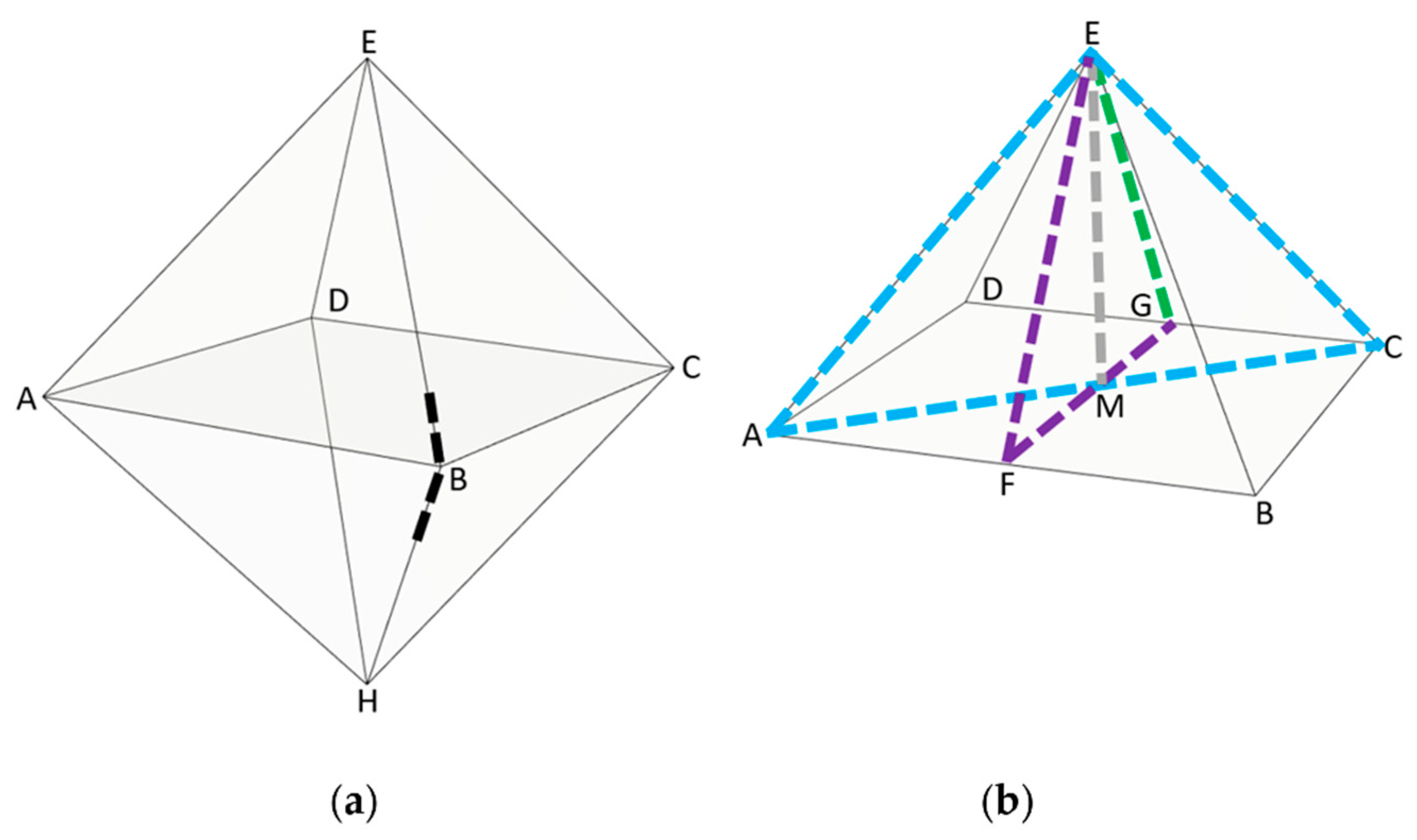
Figure 4.
(a) Octahedron as formed by {111} planes in Si. The angle indicated by the black dotted line is, by definition, 90°. (b) A pyramid cut from an octahedron. The coloured lines indicate different cross-sections of the pyramid.
Figure 4.
(a) Octahedron as formed by {111} planes in Si. The angle indicated by the black dotted line is, by definition, 90°. (b) A pyramid cut from an octahedron. The coloured lines indicate different cross-sections of the pyramid.
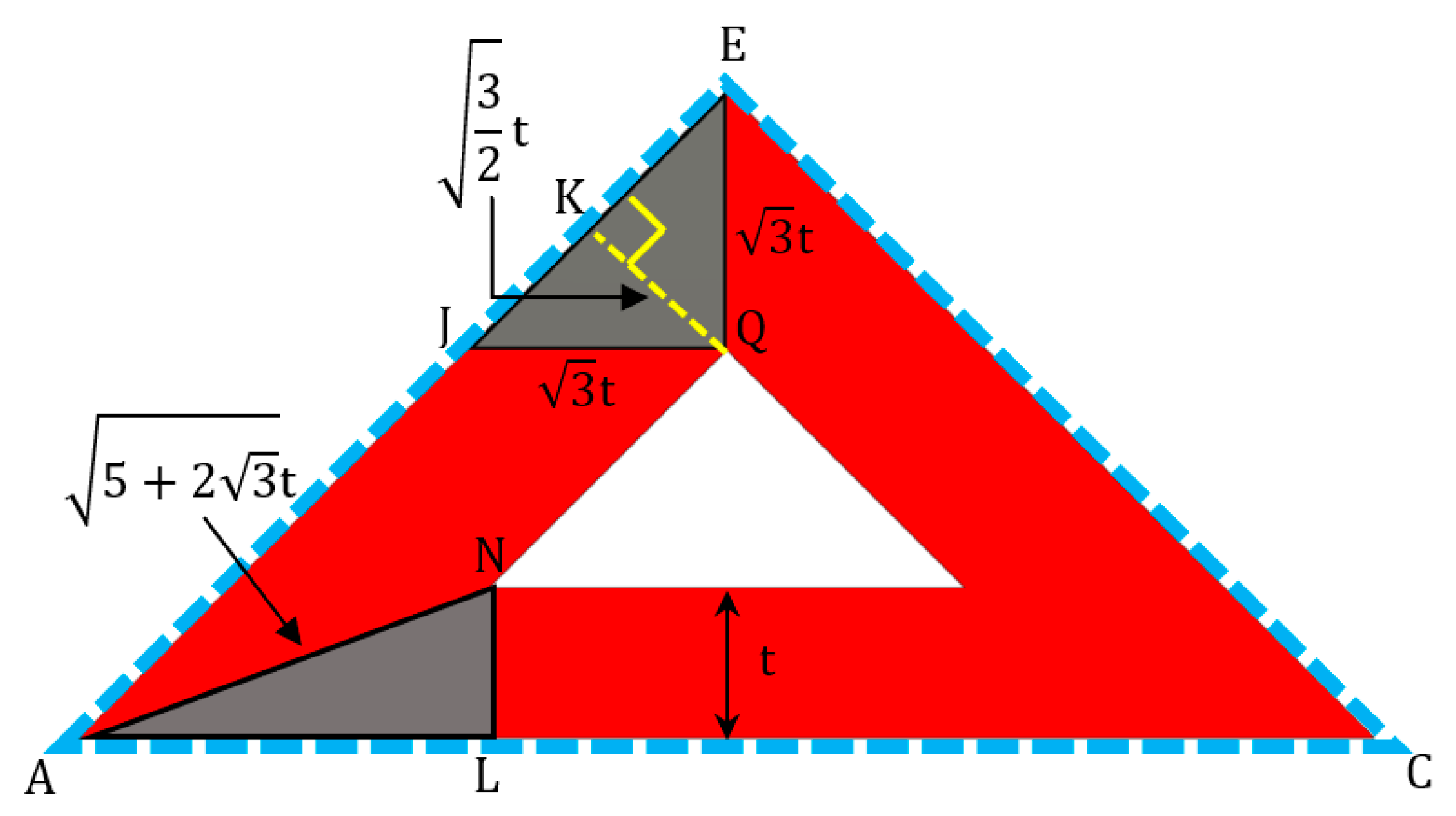
Figure 5.
Cross-section of the pyramid over the blue dashed line or through A, C, and E. The grey triangles and are used to calculate the lengths and ratios between the edges.
Figure 5.
Cross-section of the pyramid over the blue dashed line or through A, C, and E. The grey triangles and are used to calculate the lengths and ratios between the edges.
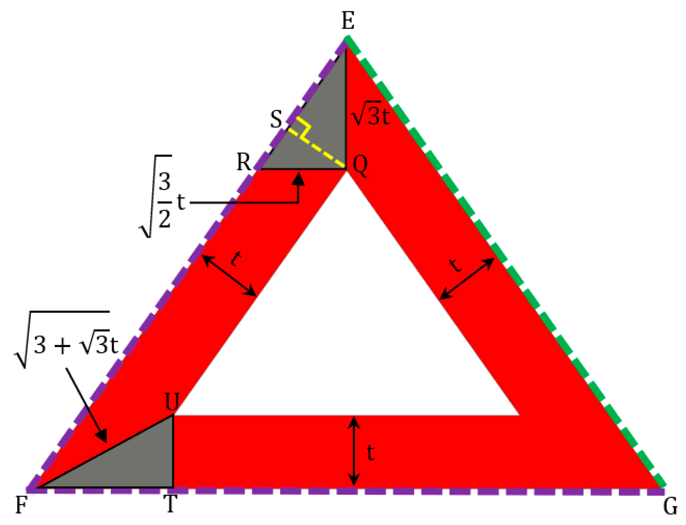
Figure 6.
Cross-section of the pyramid over the green and purple dashed line or through F, E and G. The grey triangles ΔEQR and ΔTUF are used to calculate the lengths and ratios between the edges.
Figure 6.
Cross-section of the pyramid over the green and purple dashed line or through F, E and G. The grey triangles ΔEQR and ΔTUF are used to calculate the lengths and ratios between the edges.
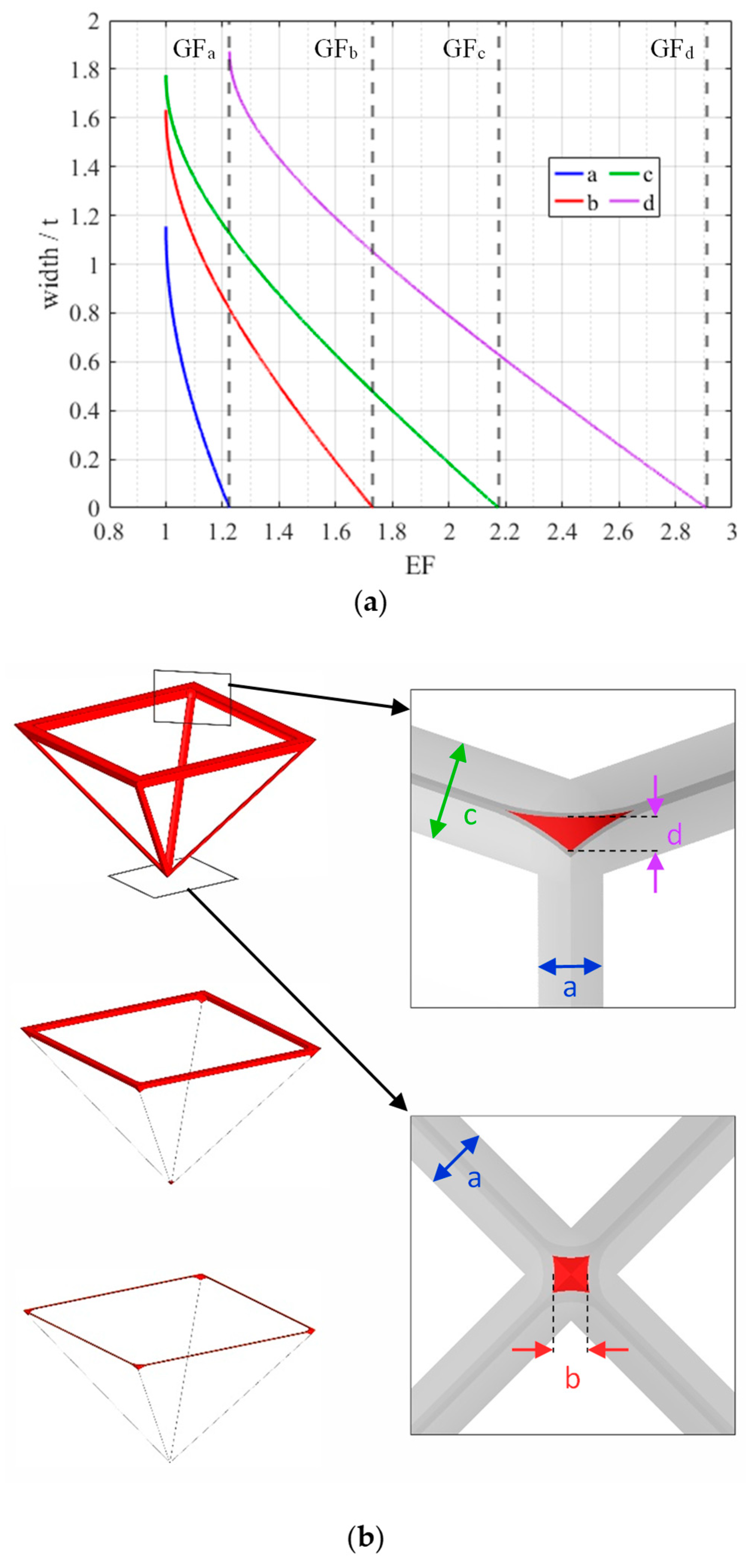
Figure 7.
(a) Feature width relative to the deposited layer thickness t vs. the etching factor EF. (b) The etched Si3N4 frame with on the right the views from inside to the apex perpendicular to its centre.
Figure 7.
(a) Feature width relative to the deposited layer thickness t vs. the etching factor EF. (b) The etched Si3N4 frame with on the right the views from inside to the apex perpendicular to its centre.
Figure 8.
First part of the process flow demonstrating various levels of CL: (
a) Si (grey) with SiO
2 hard-mask (blue) containing an etched hole. (
b) Anisotropic etching of an inverted pyramid Si using KOH via the hole in the hard-mask. (
c–
h) Cross-sections. (
c) Etched inverted pyramid. (
d) Deposition of Si
4N
4 (red) with a thickness
t. (
e) Etching of Si
3N
4 with an etching distance of t or an EF of 1 leaving an Si
3N
4 “wireframe”. (
f) Etching of Si
3N
4 with an EF of 1.35, leaving only a Si
3N
4 “ring” at the base and a nanodot at the apex of the inverted pyramid. (
g) Etching of Si
3N
4 with an EF of 2, leaving only the Si
3N
4 ring. (
h) Etching of Si
3N
4 with an EF of 2.2, leaving only nanodots at the vertices of the base of the pyramid. The dashed rectangle indicates the location of the zoom-in of
Figure 9.
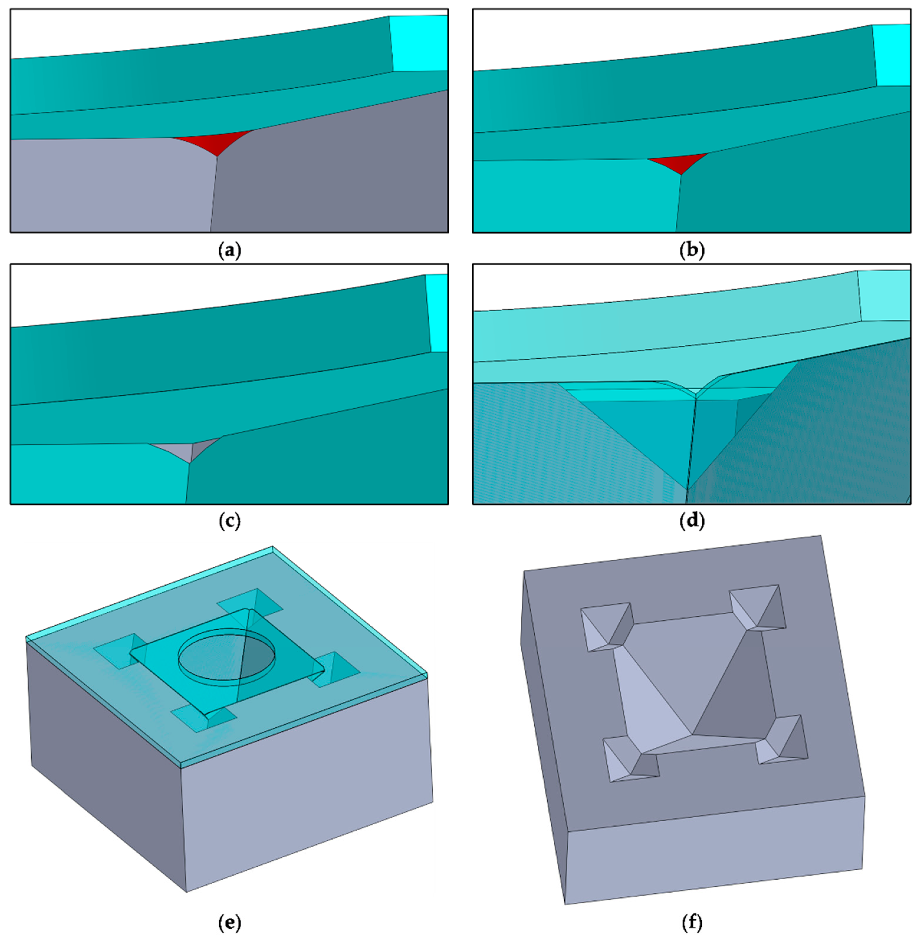
Figure 9.
Second part of the process flow demonstrating how to create the G2 fractal: (a) Enlarged vertex of the base of the pyramid with Si3N4 nanodot (red). (b) Vertex with nanodot after LOCOS of the Si (grey). (c) Vertex after etching of the nanodot. (d) Vertex after etching the Si, creating the G2 fractal. (e) Top-view of the G1 and G2 fractal under the SiO2 (blue) mask. (f) Top-view of the G1 and G2 fractal in Si without the planar hard-mask.
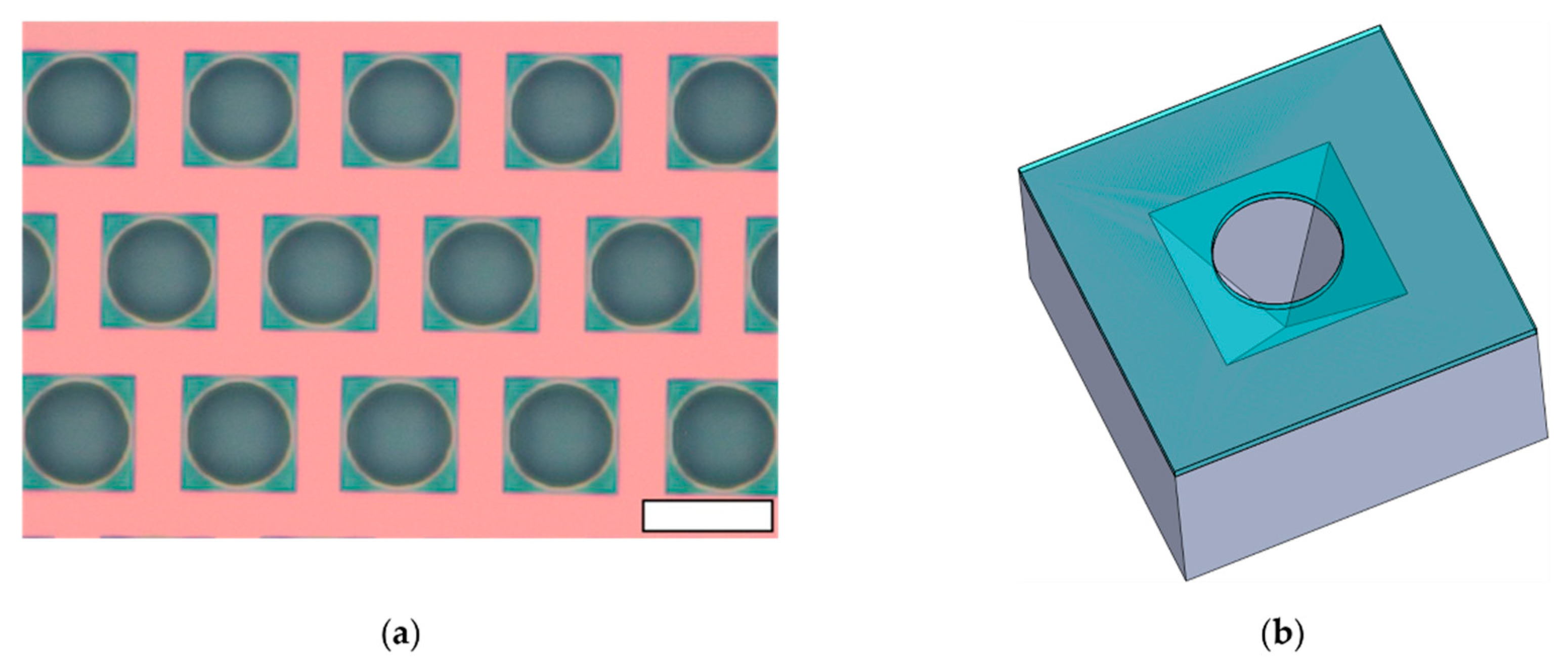
Figure 10.
(a) Top-view microscope image of the inverted pyramids etched in Si by anisotropic etching under the SiO2 hard-mask as shown in the sketch in (b) (where the SiO2 hard-mask is shown in blue). The scale-bar is 10 µm.
Figure 10.
(a) Top-view microscope image of the inverted pyramids etched in Si by anisotropic etching under the SiO2 hard-mask as shown in the sketch in (b) (where the SiO2 hard-mask is shown in blue). The scale-bar is 10 µm.
Figure 11.
Tilted SEM (a–c) images of the Si3N4 corners of the last stage of the corner lithography. (b,c) Zoomed-in images at the corner indicated by the dashed rectangles. Scalebars: (a) 2 µm and (b,c) 200 nm.
Figure 11.
Tilted SEM (a–c) images of the Si3N4 corners of the last stage of the corner lithography. (b,c) Zoomed-in images at the corner indicated by the dashed rectangles. Scalebars: (a) 2 µm and (b,c) 200 nm.
Figure 12.
G2 after 5 min of etching in TMAH (25% 70 °C). (a) Top-view taken with an optical microscope through the SiO2 hard-mask. (b) SEM image of a cross-section. (c) SEM image from the top after stripping the SiO2 hard-mask in BHF. (d) Zoom-in SEM image of the G2 Fractal after stripping the SiO2 hard-mask in BHF. Enlarged area is indicated in red. Scalebars: (a,c) 6 µm and (d) 200 nm.
Figure 13.
G2 after 125 min of etching in TMAH (25% 70 °C). (a) Top-view taken with an optical microscope through the SiO2 hard-mask. (b–e) SEM images with a tilt of 0°, 10°, 20°, and 40°, respectively, with (e) also rotated after stripping the SiO2 hard-mask for taking the images. (f) Zoom-in of a G2 of the left bottom corner with a 40° tilt. Scalebars: (a) 10 µm and (b–f) 2 µm.
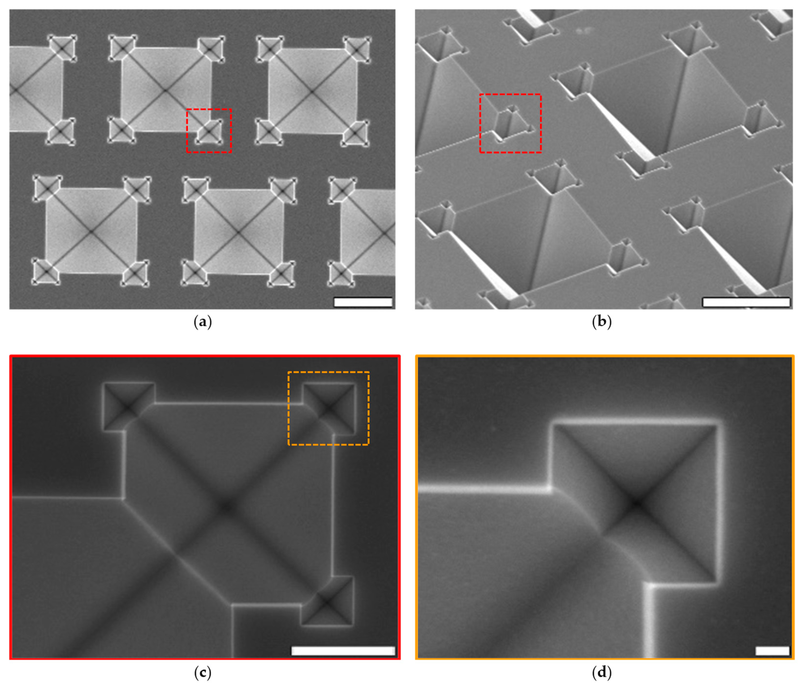
Figure 14.
Top-view SEM images (a–d) of the formation of third generation (G3) fractals after anisotropic etching in TMAH. In (b), substrate was 45° tilted. The enlarged areas are indicated by the red and orange dashed lines. Scalebars: (a,b) 5 µm, (c) 1 µm and (d) 100 nm.
Figure 14.
Top-view SEM images (a–d) of the formation of third generation (G3) fractals after anisotropic etching in TMAH. In (b), substrate was 45° tilted. The enlarged areas are indicated by the red and orange dashed lines. Scalebars: (a,b) 5 µm, (c) 1 µm and (d) 100 nm.
Figure 15.
Cross-sectional SEM view of the second (G2), third (G3), and fourth generation (G4) fractals. The cross-section is made by breaking the sample. The diagonal bent lines at the bottom are caused by the break line being not fully parallel to the crystalline lattice for taking the cross-section SEM images. The white arrow in (c) indicates in which direction etchants went through the “nozzle” in the apex of the G3 to etch the G4. Enlarged areas are indicated in red and orange dashed lines. Scalebars: (a,b) 1 µm and (c) 100 nm.
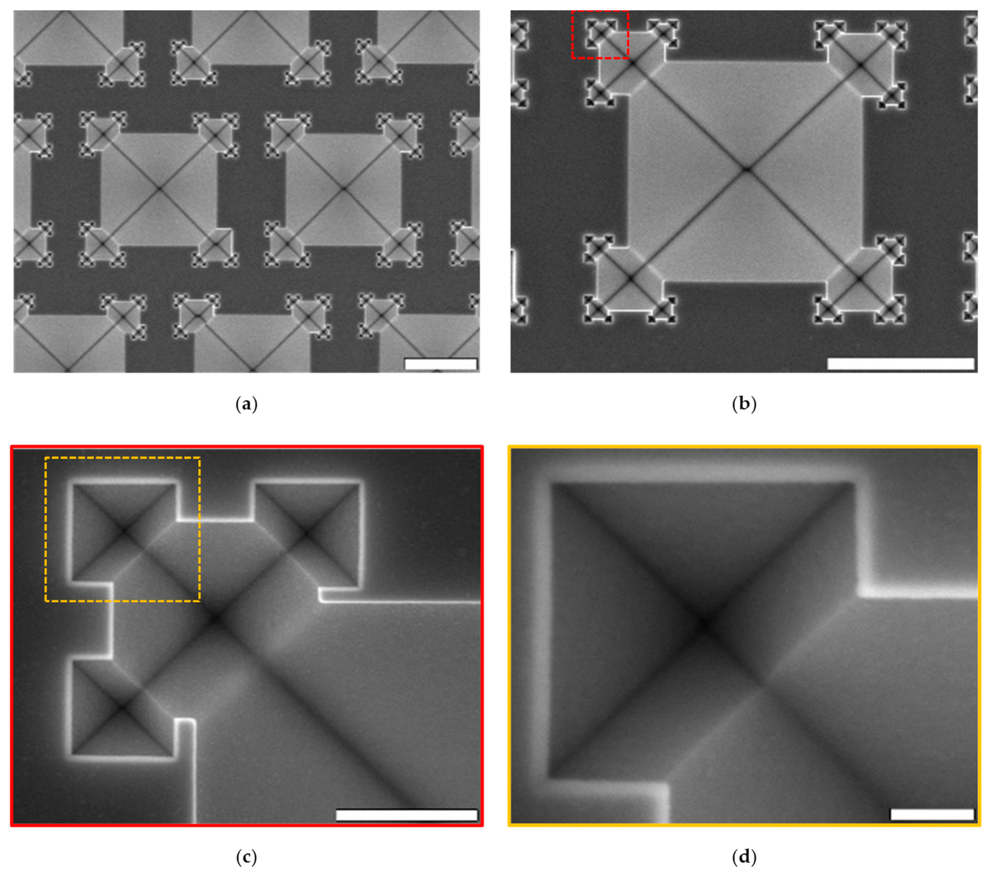
Figure 16.
SEM top-view images of the G4 in-plane fractal formation after TMAH and stripping of SiO2 layer. Enlarged areas are indicated in red and orange dashed lines. Scalebars: (a,b) 5 µm, (c) 500 nm and (d) 100 nm.
Figure 16.
SEM top-view images of the G4 in-plane fractal formation after TMAH and stripping of SiO2 layer. Enlarged areas are indicated in red and orange dashed lines. Scalebars: (a,b) 5 µm, (c) 500 nm and (d) 100 nm.
Figure 17.
SEM top-view images (a–f) of G4 in-plane fractals after final thermal oxidation and anodic bonding and back-side etching in TMAH. (d–f) Substrate was 45° tilted. Enlarged areas are indicated in coloured dashed line. The charge-up effect in the SEM image is present due to the nonconductive SiO2 layer. Enlarged areas are indicated in red and orange dashed lines. Scalebars: (a,b,d,e) 10 µm, (c) 100 nm and (f) 1 µm.
Figure 18.
(a) Undercutting of the SiO2 mask (indicated by red circle) after removing the G1 masking layer. (b) Formation of extra corner in Si by using TMAH. (c) The combined result of both effects.
Figure 18.
(a) Undercutting of the SiO2 mask (indicated by red circle) after removing the G1 masking layer. (b) Formation of extra corner in Si by using TMAH. (c) The combined result of both effects.
Figure 19.
Cross-sectional SEM showing that Si3N4 was conformally deposited prior to corner lithography on the G2 (a) and (b) zoomed section indicated in red also showing the extra etched corners as described. (c) is (b) after EF of 1.0. The white arrows indicate the undercut of the SiO2 mask. Scalebars: (a) 1 µm and (b,c) 100 nm.
Figure 20.
Cross-sectional SEM images showing corner lithography performed with (a,b) EF 1.9 inside a G3. (b) Enlarged zoom-in of the area indicated by the red dashed line. The white arrows indicates the extra corners formed in Si. Scalebars: (a) 500 nm and (b) 100 nm.
Figure 20.
Cross-sectional SEM images showing corner lithography performed with (a,b) EF 1.9 inside a G3. (b) Enlarged zoom-in of the area indicated by the red dashed line. The white arrows indicates the extra corners formed in Si. Scalebars: (a) 500 nm and (b) 100 nm.
Table 1.
Overview of the corner types and corresponding geometric factor. The letters in the Corner column correspond to those in
Figure 7.
Table 1.
Overview of the corner types and corresponding geometric factor. The letters in the Corner column correspond to those in
Figure 7.
| Corner | | Type | Geometric Factor (GF) |
|---|
| (a) | Edge | |
| ∠GEF | (b) | Vertex | |
| (c) | Edge | |
| ∠EAC | (d) | Vertex | |
Table 2.
Qualitative, relative etching characteristics of used materials in used etchants. X stands for not etching or insignificant etch rates.
Table 2.
Qualitative, relative etching characteristics of used materials in used etchants. X stands for not etching or insignificant etch rates.
| Etchants | Si3N4 | SiO2 | Si |
|---|
| 20% KOH at 21 °C | X | X | Good |
| 25% TMAH at 70 °C | X | X | Good |
| 85% H3PO4 at 180 °C | Good | Moderate | Low |
| 85% H3PO4 at 160 °C | Good | Moderate | X |
| 85% H3PO4 at 125 °C | Good | Low | X |
| 1% HF at 17 °C | X | Good | X |
| 50% HF at 17 °C | Moderate | Good | X |
Table 3.
Left: the etch factor (EF). Middle: sketch of the Si3N4 frame under the SiO2 hard-mask in the Si. Right: top-view SEM images taken from a single corner of the inverted pyramid. The scale-bars are 200 nm.
Table 3.
Left: the etch factor (EF). Middle: sketch of the Si3N4 frame under the SiO2 hard-mask in the Si. Right: top-view SEM images taken from a single corner of the inverted pyramid. The scale-bars are 200 nm.


