
Dimensional Accuracy of Electron Beam Powder Bed Fusion with Ti-6Al-4V

Abstract
:1. Introduction
2. Materials and Methods
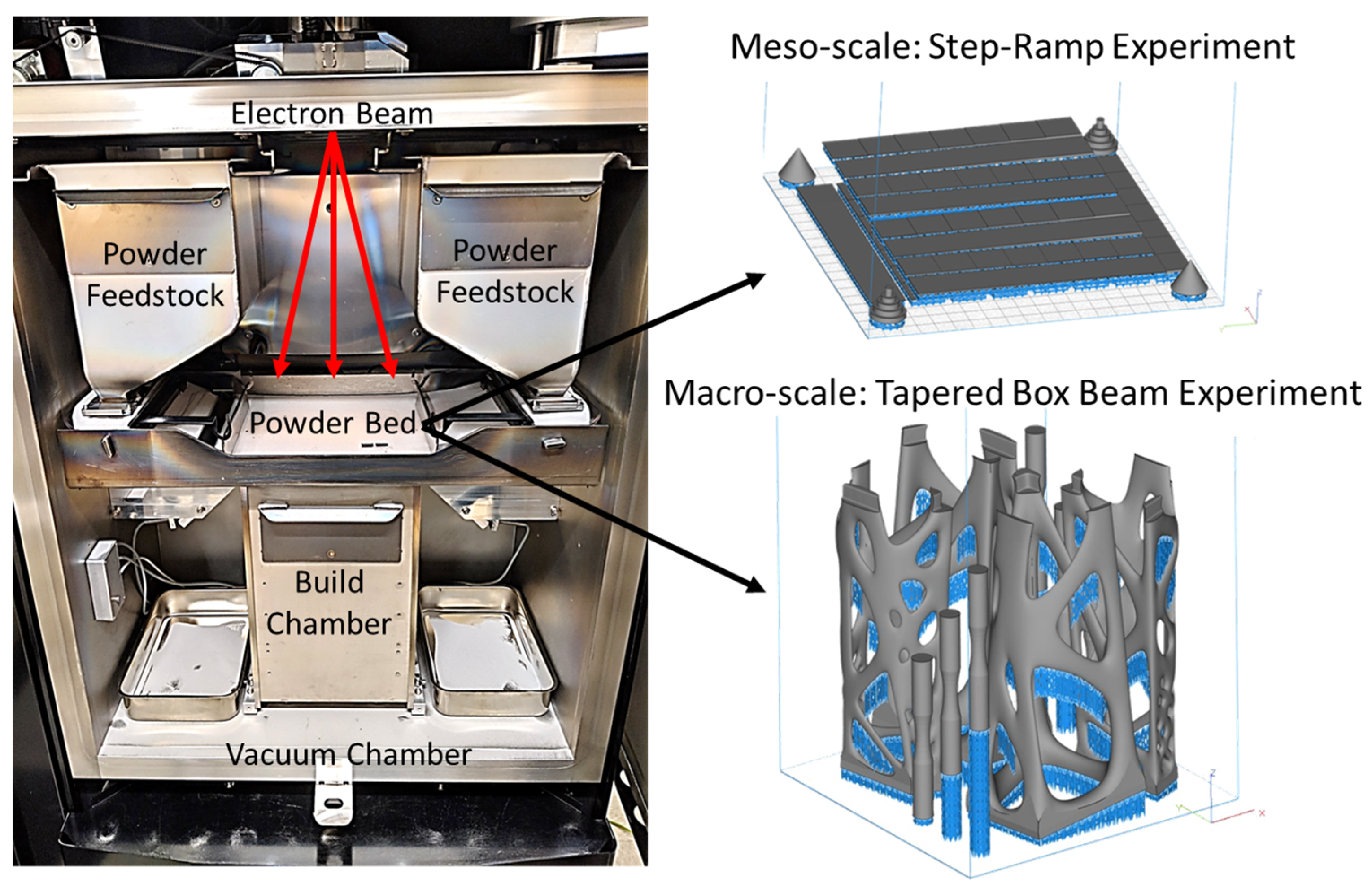
2.1. EB-PBF Process
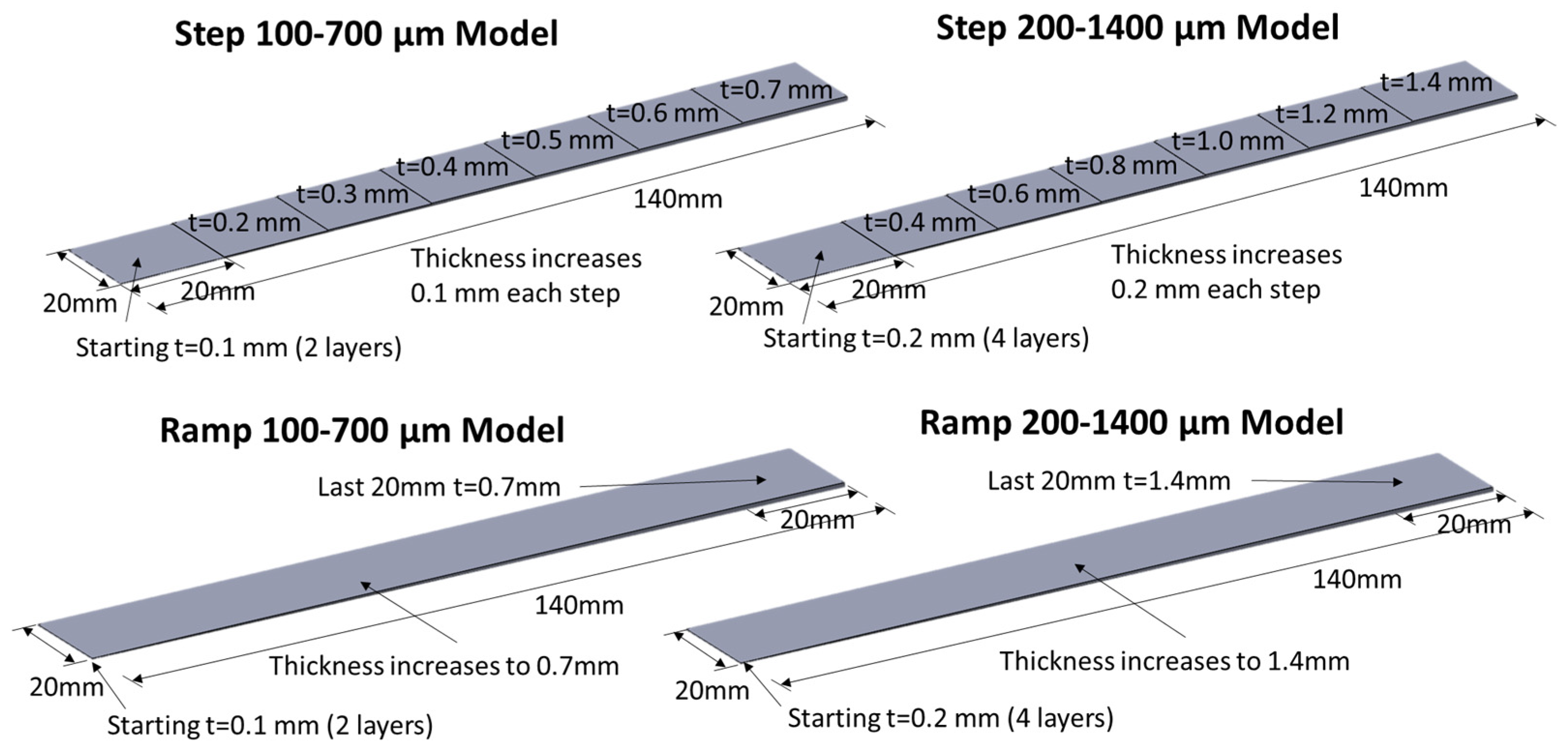
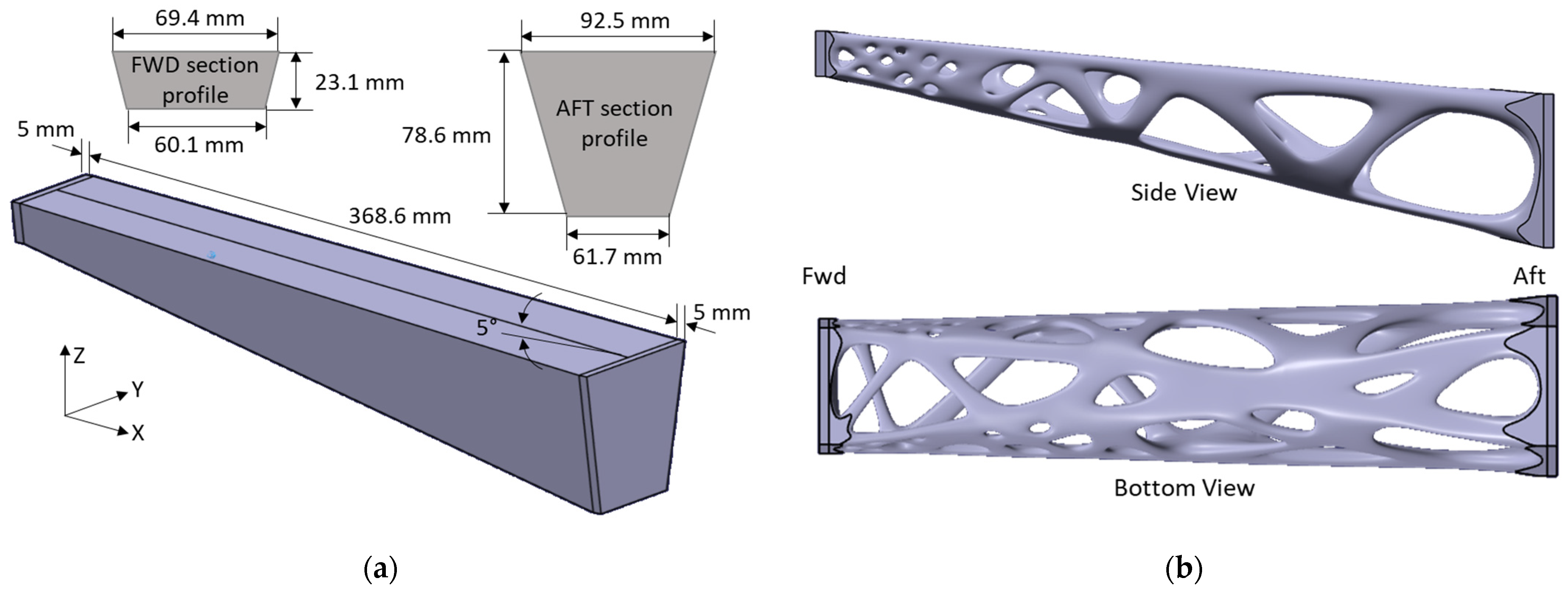
2.2. Experimental Design
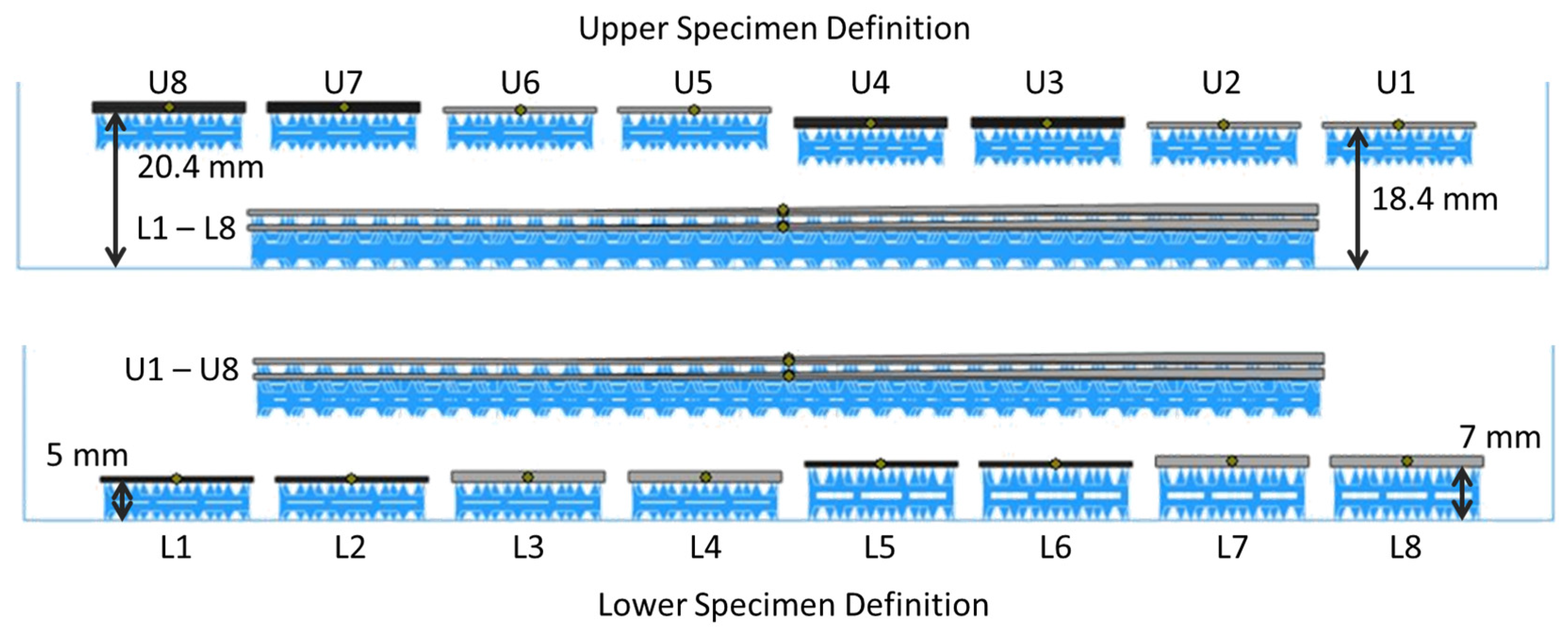
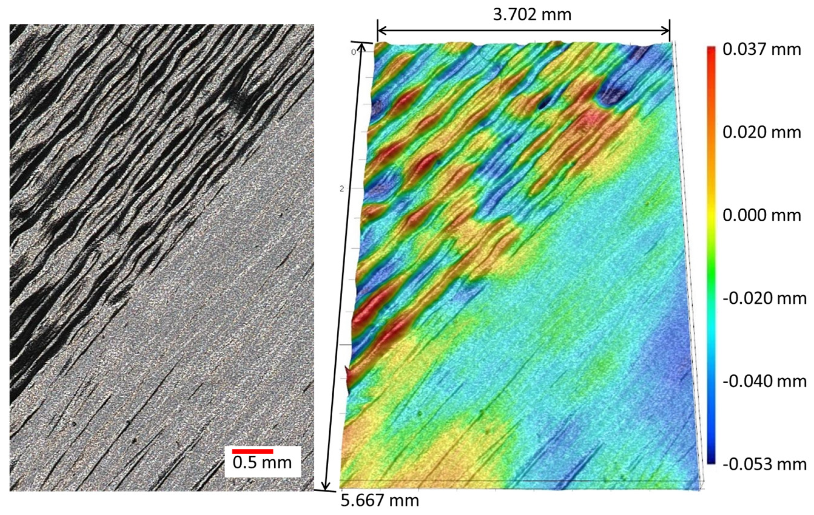
2.3. Metrology
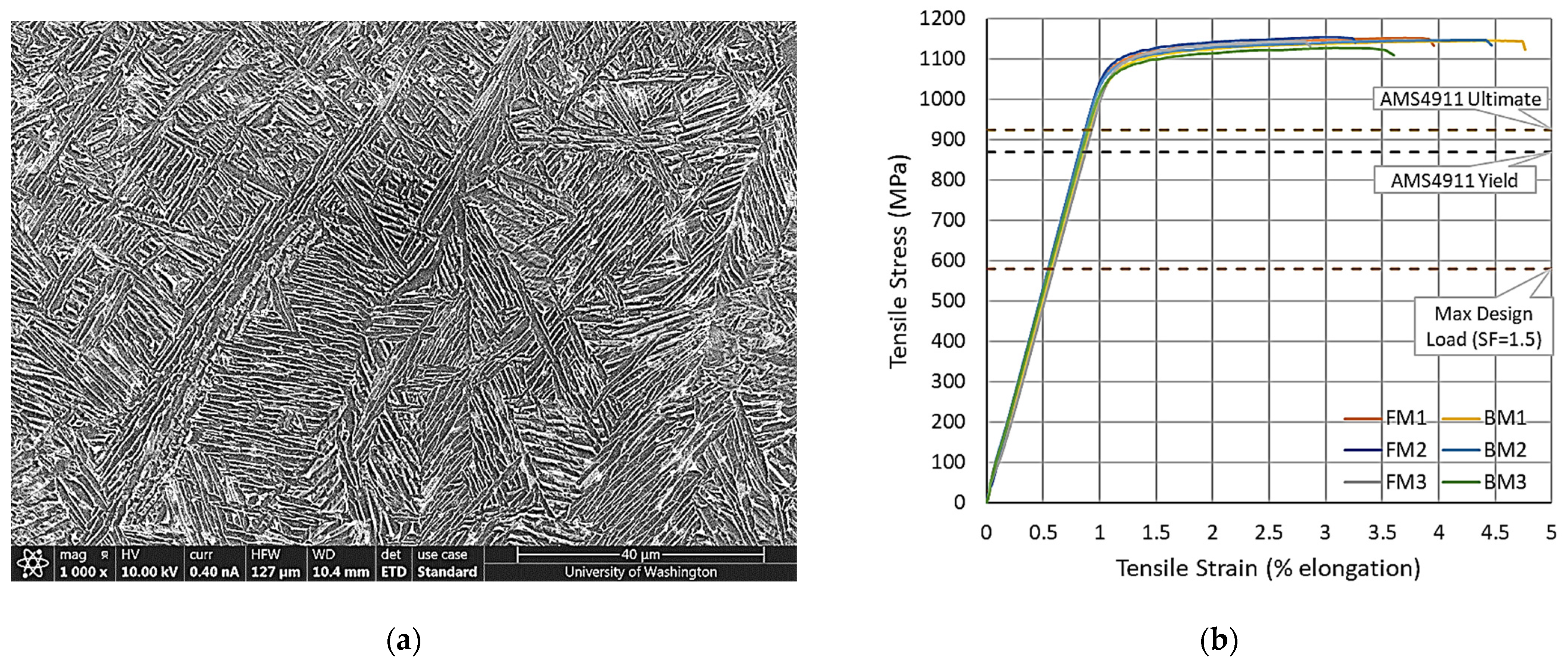
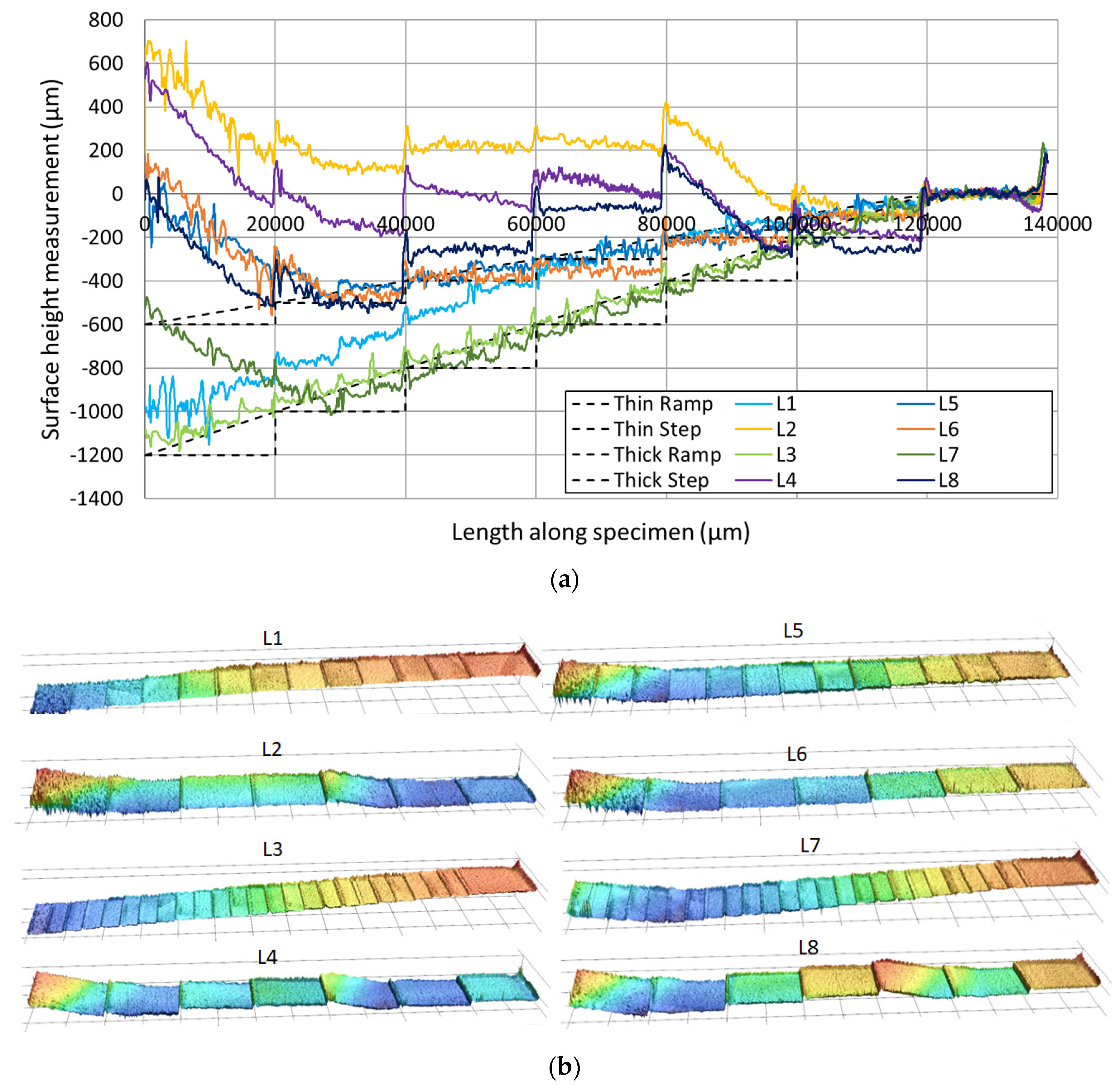
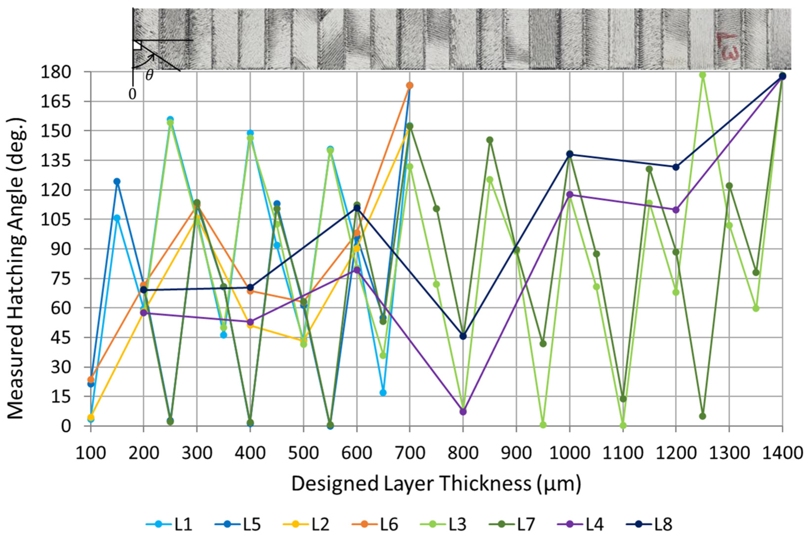
3. Results
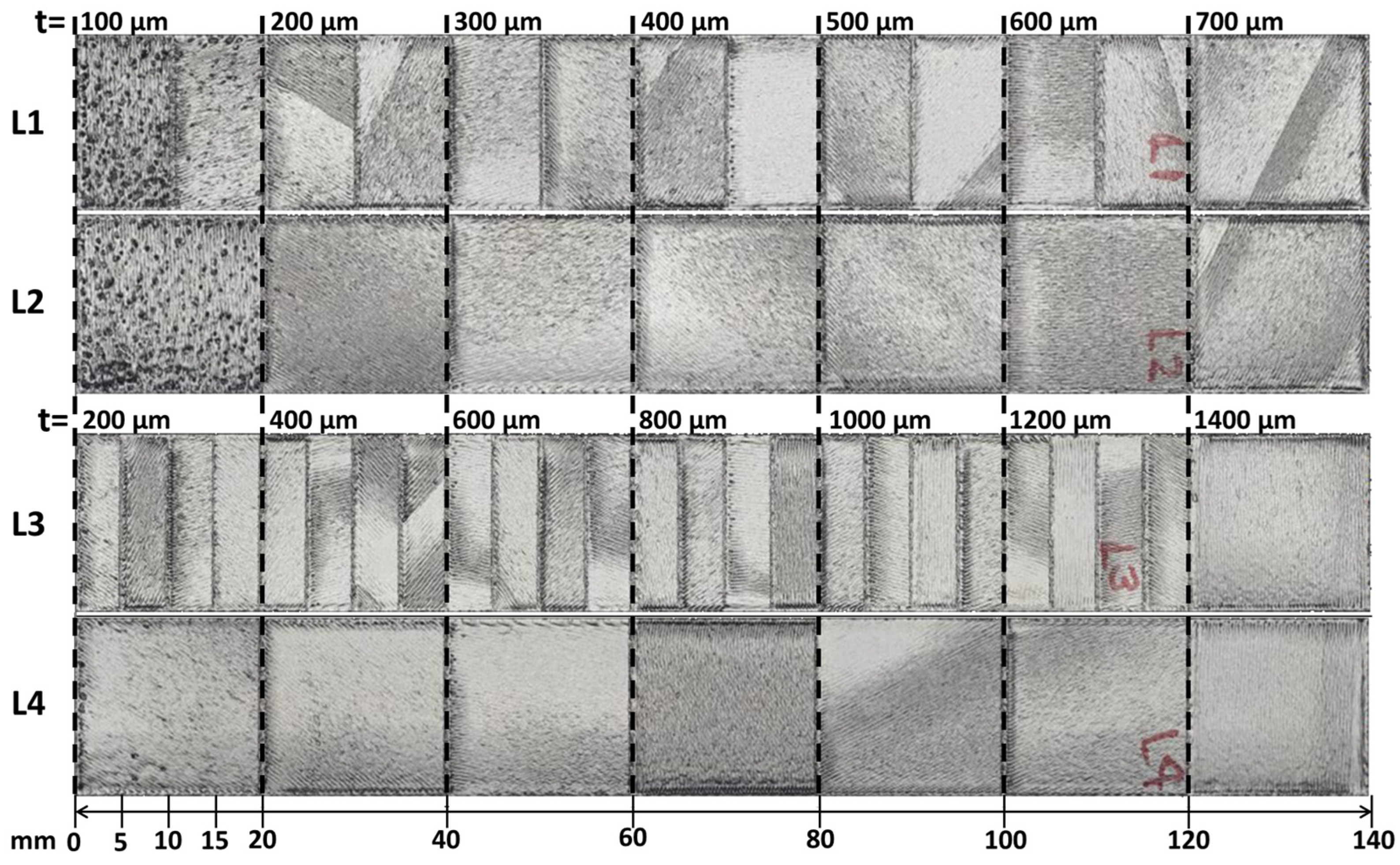
3.1. Meso-Scale Step-Ramp Experiment
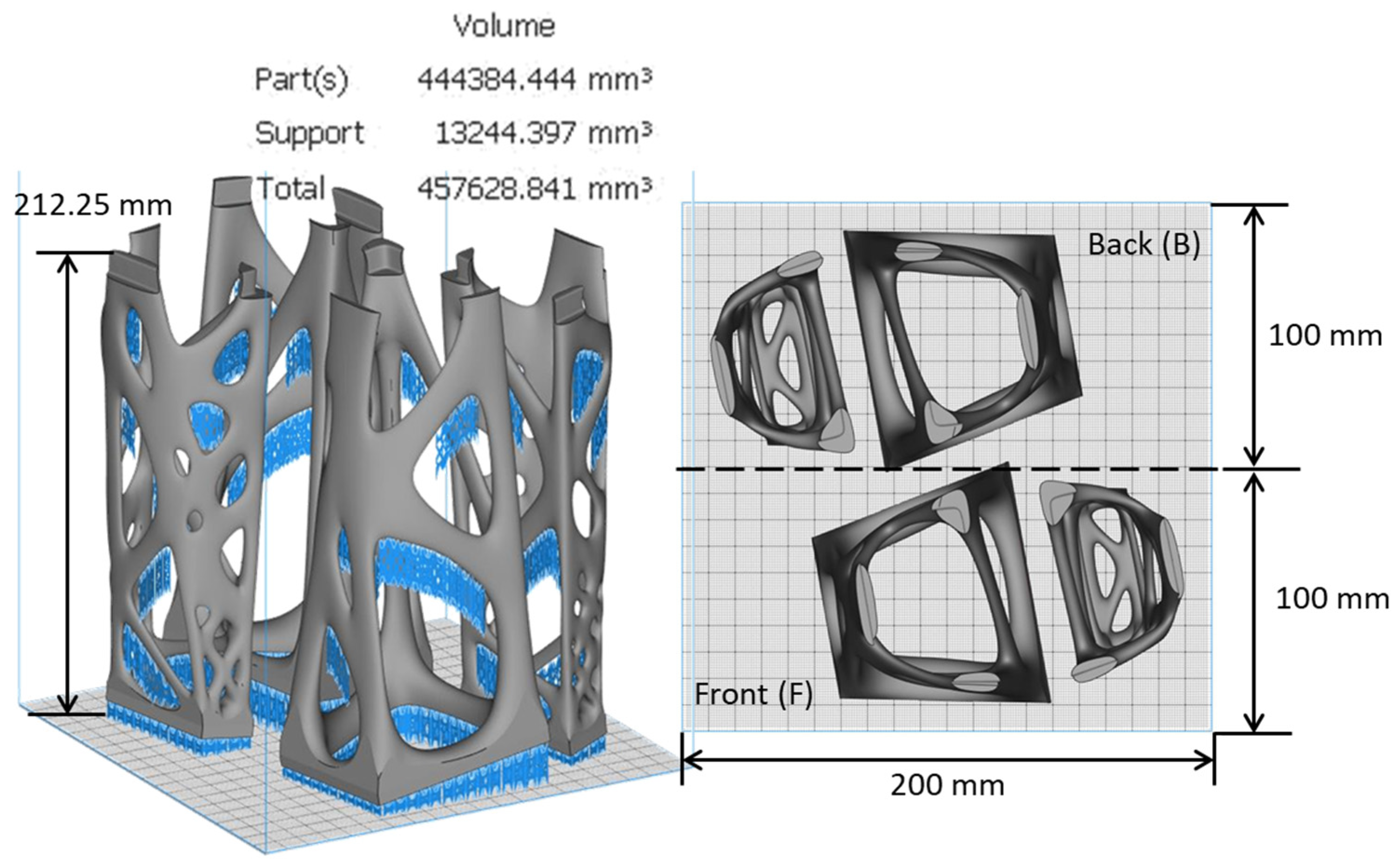
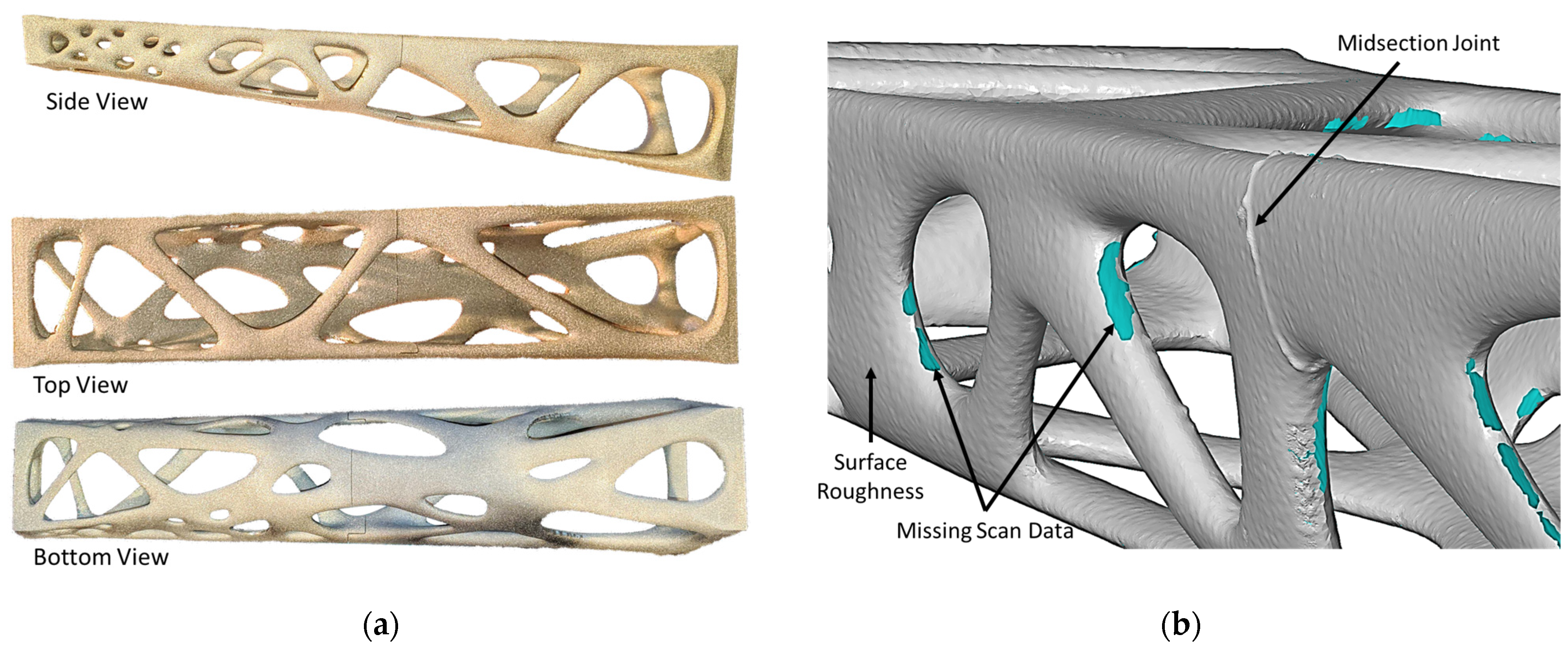
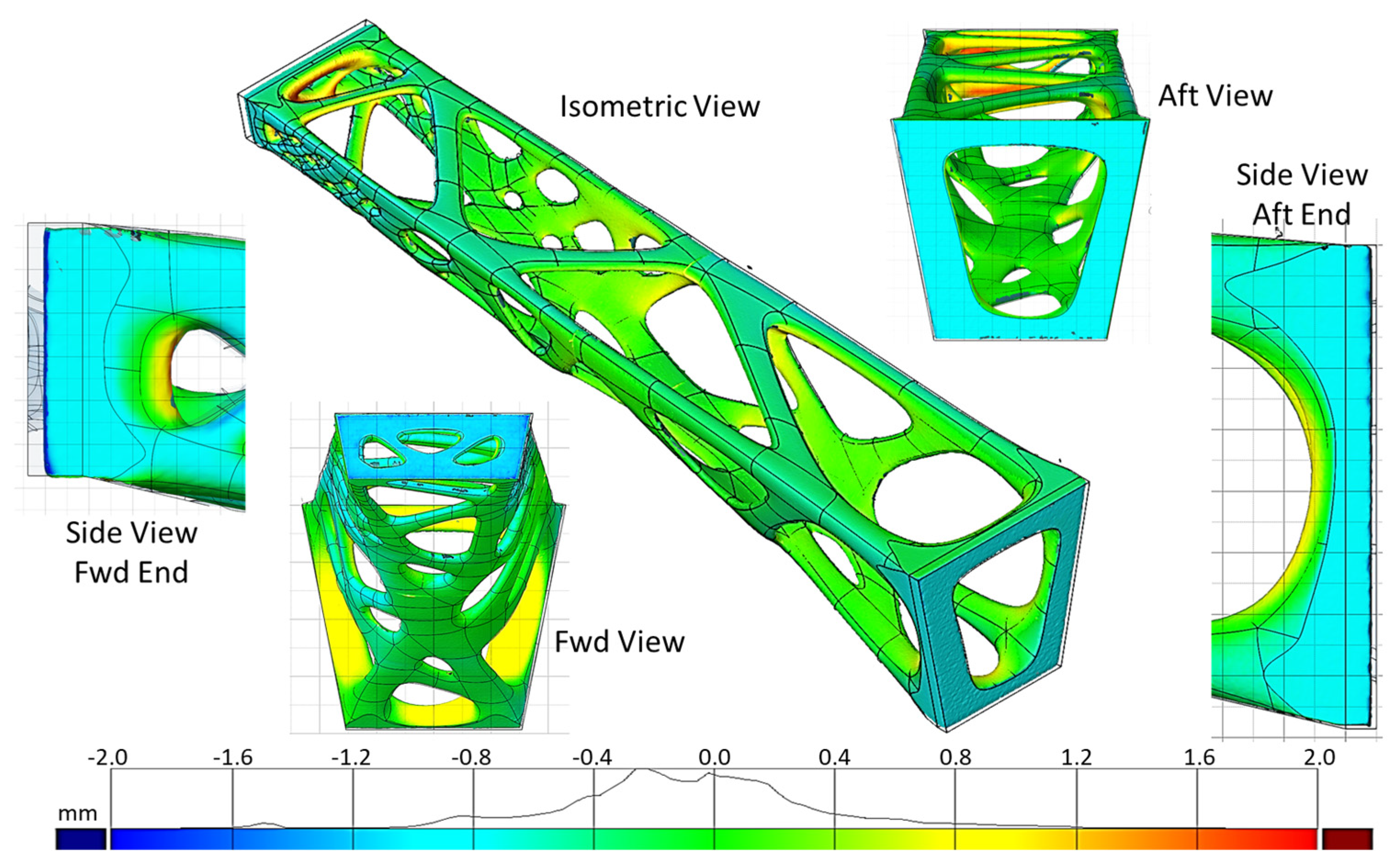
3.2. Macro-Scale Beam Experiment
4. Discussion
5. Conclusions
- for thin samples of the same geometry, different hatching histories reduced the dimensional accuracy, causing random deviations many times the thickness, up to 4 mm;
- for large models of the same geometry, the range of dimensional deviation across three builds was 0.26 mm;
- the average 2.3 mm deviation from the nominal geometry could have been mitigated if the tapered box beam models had been compensated for thermal expansion using a of 625 °C;
- a high degree of geometric accuracy at the assembly level was demonstrated with a modeled interface clearance of 0.1 mm.
Author Contributions
Funding
Data Availability Statement
Acknowledgments
Conflicts of Interest
References
- Seepersad, C.C. Challenges and Opportunities in Design for Additive Manufacturing. 3D Print. Addit. Manuf. 2014, 1, 10–13. [Google Scholar] [CrossRef]
- Persenot, T.; Burr, A.; Martin, G.; Buffiere, J.-Y.; Dendievel, R.; Maire, E. Effect of build orientation on the fatigue properties of as-built Electron Beam Melted Ti-6Al-4V alloy. Int. J. Fatigue 2019, 118, 65–76. [Google Scholar] [CrossRef]
- Riedlbauer, D.; Scharowsky, T.; Singer, R.F.; Steinmann, P.; Körner, C.; Mergheim, J. Macroscopic simulation and experimental measurement of melt pool characteristics in selective electron beam melting of Ti-6Al-4V. Int. J. Adv. Manuf. Technol. 2017, 88, 1309–1317. [Google Scholar] [CrossRef] [Green Version]
- Boone, N.; Zhu, C.; Smith, C.; Todd, I.; Willmott, J. Thermal near infrared monitoring system for electron beam melting with emissivity tracking. Addit. Manuf. 2018, 22, 601–605. [Google Scholar] [CrossRef]
- Landau, E.; Tiferet, E.; Ganor, Y.; Ganeriwala, R.; Matthews, M.; Braun, D.; Chonin, M.; Ziskind, G. Thermal characterization of the build chamber in electron beam melting. Addit. Manuf. 2020, 36, 101535. [Google Scholar] [CrossRef]
- Wojtuszewski, R.; Banas, A.; Oliwa, M. Additive manufacturing of titanium alloys. In Annual Forum Proceedings; AHS International: Fairfax, VA, USA, 2018; pp. 1–18. [Google Scholar]
- Sames, W.J.; List, F.A.; Pannala, S.; Dehoff, R.R.; Babu, S.S. The metallurgy and processing science of metal additive manufacturing. Int. Mater. Rev. 2016, 61, 315–360. [Google Scholar] [CrossRef]
- Cordero, Z.C.; Meyer, H.M.; Nandwana, P.; Dehoff, R.R. Powder bed charging during electron-beam additive manufacturing. Acta Mater. 2017, 124, 437–445. [Google Scholar] [CrossRef] [Green Version]
- Zhao, X.; Dadbakhsh, S.; Rashid, A. Contouring strategies to improve the tensile properties and quality of EBM printed Inconel 625 parts. J. Manuf. Process. 2021, 62, 418–429. [Google Scholar] [CrossRef]
- Körner, C. Additive manufacturing of metallic components by selective electron beam melting—A review. Int. Mater. Rev. 2016, 61, 361–377. [Google Scholar] [CrossRef] [Green Version]
- Townsend, A.; Senin, N.; Blunt, L.; Leach, R.K.; Taylor, J.S. Surface texture metrology for metal additive manufacturing: A review. Precis. Eng. 2016, 46, 34–47. [Google Scholar] [CrossRef] [Green Version]
- Newton, L.; Senin, N.; Chatzivagiannis, E.; Smith, B.; Leach, R. Feature-based characterisation of Ti6Al4V electron beam powder bed fusion surfaces fabricated at different surface orientations. Addit. Manuf. 2020, 35, 101273. [Google Scholar] [CrossRef]
- Lee, S.; Rasoolian, B.; Silva, D.F.; Pegues, J.W.; Shamsaei, N. Surface roughness parameter and modeling for fatigue behavior of additive manufactured parts: A non-destructive data-driven approach. Addit. Manuf. 2021, 46, 102094. [Google Scholar] [CrossRef]
- Flys, O.; Berglund, J.; Rosén, B.-G. Using confocal fusion for measurement of metal AM surface texture. Surf. Topogr. Metrol. Prop. 2020, 8, 024003. [Google Scholar] [CrossRef]
- Lou, S.; Zhu, Z.; Zeng, W.; Majewski, C.; Scott, P.J.; Jiang, X. Material ratio curve of 3D surface topography of additively manufactured parts: An attempt to characterise open surface pores. Surf. Topogr. Metrol. Prop. 2021, 9, 015029. [Google Scholar] [CrossRef]
- Thompson, A.; Senin, N.; Giusca, C.; Leach, R. Topography of selectively laser melted surfaces: A comparison of different measurement methods. CIRP Ann. Manuf. Technol. 2017, 66, 543–546. [Google Scholar] [CrossRef]
- Wang, P.; Sin, W.J.; Nai, M.L.S.; Wei, J. Effects of Processing Parameters on Surface Roughness of Additive Manufactured Ti-6Al-4V via Electron Beam Melting. Materials 2017, 10, 1121. [Google Scholar] [CrossRef] [PubMed] [Green Version]
- Seewig, J.; Scott, P.J.; Eifler, M.; Barwick, B.; Hüser, D. Crossing-The-Line Segmentation as a Basis for Rsm and Rc Evaluation. Surf. Topogr. Metrol. Prop. 2020, 8, 024010. [Google Scholar] [CrossRef]
- Bukkapatnam, S.T.; Iquebal, A.S.; Kumara, S.R. Planar random graph representations of spatiotemporal surface morphology: Application to finishing of 3-D printed components. CIRP Ann. 2018, 67, 495–498. [Google Scholar] [CrossRef]
- Du Plessis, A.; Tshibalanganda, M.; Yadroitsava, I.; Yadroitsev, I. On the Evaluation of Surface Roughness: X-ray Tomography Reveals Hidden Details. In Progress in Additive Manufacturing 2020; Shamsaei, N., Seifi, M., Eds.; ASTM International: West Conshohocken, PA, USA, 2022; pp. 208–222. [Google Scholar]
- Gao, W.; Zhang, Y.; Ramanujan, D.; Ramani, K.; Chen, Y.; Williams, C.B.; Wang, C.C.L.; Shin, Y.C.; Zhang, S.; Zavattieri, P.D. The status, challenges, and future of additive manufacturing in engineering. Comput.-Aided Des. 2015, 69, 65–89. [Google Scholar] [CrossRef]
- Marrugo, A.G.; Gao, F.; Zhang, S. State-of-the-art active optical techniques for three-dimensional surface metrology: A review. J. Opt. Soc. Am. A 2020, 37, B60. [Google Scholar] [CrossRef]
- Leach, R.; Bourell, D.; Carmignato, S.; Donmez, A.; Senin, N.; Dewulf, W. Geometrical metrology for metal additive manufacturing. CIRP Ann. 2019, 68, 677–700. [Google Scholar] [CrossRef]
- Smith, C.; Derguti, F.; Nava, E.H.; Thomas, M.; Tammas-Williams, S.; Gulizia, S.; Fraser, D.; Todd, I. Dimensional accuracy of Electron Beam Melting (EBM) additive manufacture with regard to weight optimized truss structures. J. Mater. Process. Technol. 2016, 229, 128–138. [Google Scholar] [CrossRef] [Green Version]
- Ameta, G.; Fox, J.; Witherell, P. Tolerancing and Verification of Additive Manufactured Lattice with Supplemental Surfaces. Procedia CIRP 2018, 75, 69–74. [Google Scholar] [CrossRef]
- Gruber, S.; Grunert, C.; Riede, M.; López, E.; Marquardt, A.; Brueckner, F.; Leyens, C. Comparison of dimensional accuracy and tolerances of powder bed based and nozzle based additive manufacturing processes. J. Laser Appl. 2020, 32, 032016. [Google Scholar] [CrossRef]
- Bol, E.; Doyle, C.; Ramulu, M. Process Parameter Effects on Melt Topology and Dimensional Deviation in Electron Beam Melted Ti-6Al-4V. In Proceedings of the ASME 2021 International Mechanical Engineering Congress and Exposition, Virtual, 1–5 November 2021; American Society of Mechanical Engineers: New York, NY, USA, 2021; Volume 85550, p. V02AT02A011. [Google Scholar]
- Bol, E.; Ramulu, M. Repeatability of a Topology Optimized Tapered Box Beam Additively Manufactured with Electron Beam Melted Ti-6Al-4V. In Proceedings of the ASME 2020 International Mechanical Engineering Congress and Exposition, Virtual, 16–19 November 2020; American Society of Mechanical Engineers: New York, NY, USA, 2020; Volume 84485, p. V02AT02A049. [Google Scholar]
- Zhang, X.; Leary, M.; Tang, H.; Song, T.; Qian, M. Selective electron beam manufactured Ti-6Al-4V lattice structures for orthopedic implant applications: Current status and outstanding challenges. Curr. Opin. Solid State Mater. Sci. 2018, 22, 75–99. [Google Scholar] [CrossRef]
- Damri, E.; Tiferet, E.; Braun, D.; Ganor, Y.; Chonin, M.; Orion, I. Effects of Gas Pressure during Electron Beam Energy Deposition in the EBM Additive Manufacturing Process. Metals 2021, 11, 601. [Google Scholar] [CrossRef]
- Bendsøe, M.P. Optimal shape design as a material distribution problem. Struct. Optim. 1989, 1, 193. [Google Scholar] [CrossRef]
- Zhou, M.; Rozvany, G. The COC algorithm, Part II: Topological, geometrical and generalized shape optimization. Comput. Methods Appl. Mech. Eng. 1991, 89, 309–336. [Google Scholar] [CrossRef]
- Mlejnek, H.P. Some aspects of the genesis of structures. Struct. Optim. 1992, 5, 64–69. [Google Scholar] [CrossRef]
- Muñoz, D.; Nadal, E.; Albelda, J.; Chinesta, F.; Ródenas, J. Allying topology and shape optimization through machine learning algorithms. Finite Elem. Anal. Des. 2022, 204, 103719. [Google Scholar] [CrossRef]
- Zhang, L.-C.; Wang, J.; Liu, Y.; Jia, Z.; Liang, S.-X. Additive manufacturing of titanium alloys. In Reference Module in Materials Science and Materials Engineering; Elsevier: Amsterdam, The Netherlands, 2020. [Google Scholar]


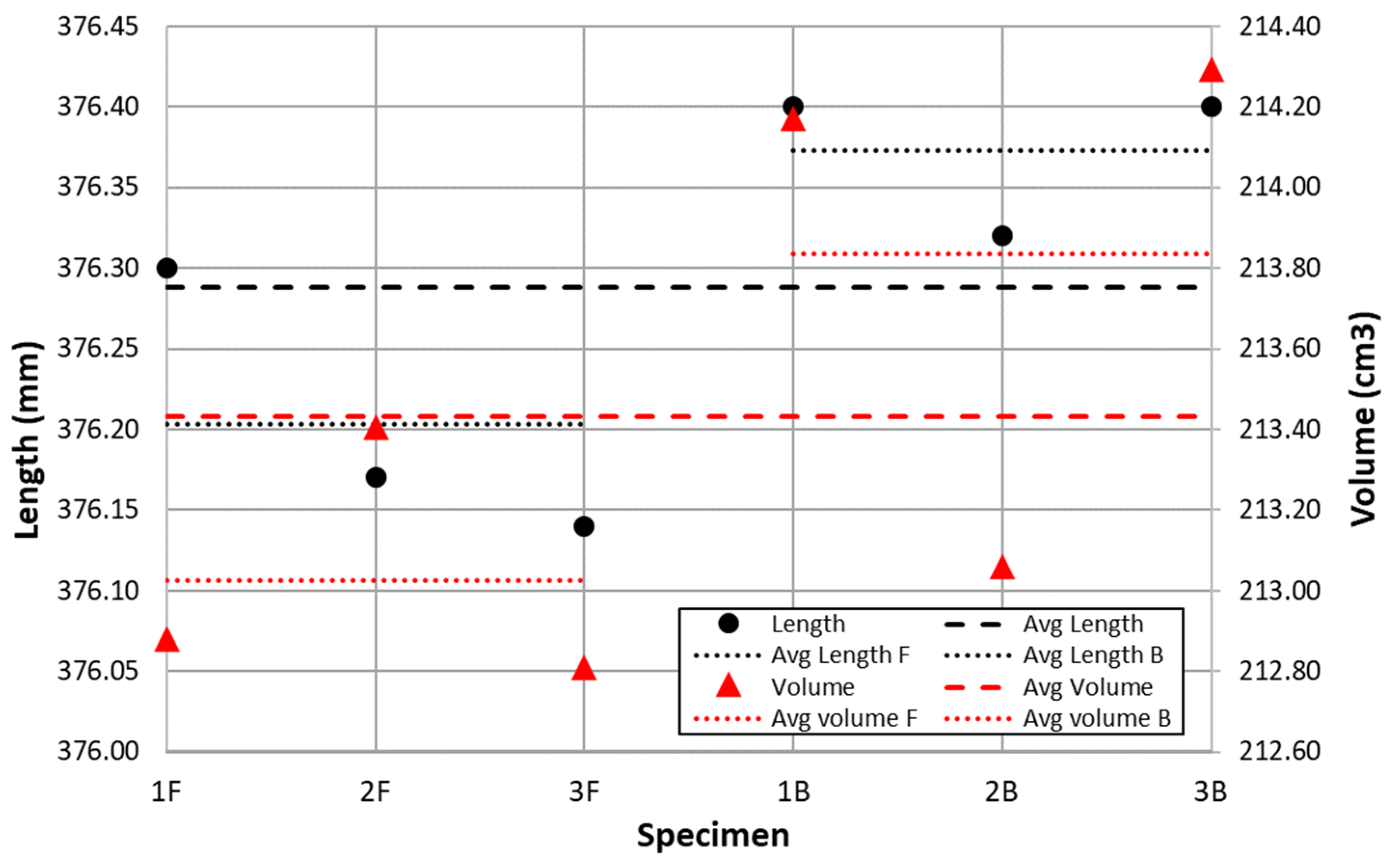
| Specimen Group | Length (mm) | Volume (cm3) |
|---|---|---|
| Avg. Front (F) | 376.20 | 213.03 |
| Range Front (F) | 0.16 | 0.60 |
| Std. Dev. Front (F) | 0.07 | 0.27 |
| Avg. Back (B) | 376.37 | 213.83 |
| Range Back (B) | 0.08 | 1.24 |
| Std. Dev. Back (B) | 0.04 | 0.55 |
| Delta Avg. (F−B) | −0.17 | −0.81 |
| Delta Std. Dev. (F−B) | 0.03 | −0.29 |
| CAD Nominal | 378.59 | 222.11 |
Disclaimer/Publisher’s Note: The statements, opinions and data contained in all publications are solely those of the individual author(s) and contributor(s) and not of MDPI and/or the editor(s). MDPI and/or the editor(s) disclaim responsibility for any injury to people or property resulting from any ideas, methods, instructions or products referred to in the content. |
© 2023 by the authors. Licensee MDPI, Basel, Switzerland. This article is an open access article distributed under the terms and conditions of the Creative Commons Attribution (CC BY) license (https://creativecommons.org/licenses/by/4.0/).
Share and Cite
Bol, E.; Ramulu, M. Dimensional Accuracy of Electron Beam Powder Bed Fusion with Ti-6Al-4V. Designs 2023, 7, 53. https://doi.org/10.3390/designs7020053
Bol E, Ramulu M. Dimensional Accuracy of Electron Beam Powder Bed Fusion with Ti-6Al-4V. Designs. 2023; 7(2):53. https://doi.org/10.3390/designs7020053
Chicago/Turabian StyleBol, Eric, and Mamidala Ramulu. 2023. "Dimensional Accuracy of Electron Beam Powder Bed Fusion with Ti-6Al-4V" Designs 7, no. 2: 53. https://doi.org/10.3390/designs7020053