Article

Analytical Model for Evaluating the Reliability of Vias and Plated Through-Hole Pads on PCBs

by
Maksim A. Korobkov
,
Fedor V. Vasilyev
* and
Olga V. Khomutskaya
Department of Digital Technologies and Information Systems, Moscow Aviation Institute, National Research University, 125993 Moscow, Russia
*
Author to whom correspondence should be addressed.
Inventions 2023, 8(3), 77; https://doi.org/10.3390/inventions8030077
Submission received: 8 May 2023 / Revised: 24 May 2023 / Accepted: 29 May 2023 / Published: 31 May 2023
(This article belongs to the Special Issue Recent Advances and New Trends in Signal Processing)

Abstract

:
Currently, there is a need to increase the density of interconnections on printed circuit boards (PCBs). Does this mean that the only option for quality PCB manufacturing is to proportionally increase precision of equipment, or is there another way? One of the main constraints on increasing the density of PCB interconnections is posed by the transition holes. As the number of conductive layers increases, the number of vias increases and they cover a significant space on the PCB. On the other hand, reducing the size of the vias is limited by the capability of spatial alignment of the PCB stack during manufacturing. There are standards that set limits for the design of contact pads on a PCB (IPC-A-600G, IPC-6012B). However, depending on the precision of production, the contact pads may be of poor quality. This raises the issue of determining the reliability of a contact pad with defined parameters at the design stage, taking into account manufacturing capabilities. This research proposes an analytical method for evaluation of reliability of a via or plated through-hole based on calculation of its probability of production in accordance with the current standards. On the basis of the method, a model was developed both for the case of a contact pad without any conductors connected to it (nonfunctional contact pad) and for the real case with a connected conductor. The model estimates the probability of making an acceptable via for a given reliability class depending on parameters such as the conductor width (minimum permissible and usable), drilled hole diameter, and pad diameter, as well as the accuracy of the drilling operation. The analysis of the modeling results showed that for the real case, a reduction in the reliability class would insignificantly affect the probability of making an acceptable via due to the tight limitation on the connection place of the conductor and the contact pad. In conclusion, we propose an algorithm for determining the optimal parameters of teardrops to minimize the negative impact of the conductor on the reliability of the vias.

1. Introduction

Modern industrial systems make it possible to produce in large volumes PCBs that meet the strictest requirements for their reliability. However, there are also a number of companies, including our department, for which the manufacture of PCBs is not their primary activity. Companies of such a format are various design centers for electronics, as it is easier, faster, and cheaper to make prototypes on their own manufacturing line. It is typical for these companies to have equipment without high-accuracy characteristics, but does this mean that high-precision and high-reliability boards are not available for production on it? What can be done when designing boards to be able to produce PCBs on affordable equipment?
The creation of modern electronic equipment is tightly linked to the development of new methods of PCB manufacturing. At present, the electronics industry is moving in the direction of increasing performance and functionality. At the same time, the requirements for the mass and dimension parameters of the produced equipment are getting more and more complicated. Increasing integration of integrated circuits leads to higher density of leads on the package, which drives the search for new design solutions in their layout [1,2,3].
To increase the functionality of the device [4] while maintaining its size, it is necessary to increase the density of the PCB interconnections, which involves increasing the number of PCB layers and, accordingly, the number of vias. The main obstacle to increasing the interconnection density consists in the large annular rings of vias, as they reduce the trace space on PCBs [5,6]. The greater the errors in the dimensional alignment of the interconnections, the larger the contact pads must be to ensure that the drill hits them reliably when obtaining the vias [7,8]. Therefore, at present, the actual issue is determining the reliability of the vias at the design stage, depending on its parameters and on the PCB manufacturing process. Currently, two main approaches to reliability estimation can be highlighted [9]: probabilistic–statistical and physico-chemical.
In the first approach (probabilistic–statistical), the main index of reliability is failure rate, which is determined with the statistical data [10,11,12,13]. However, as the reliability of electronics elements increases, the processes of determining reliability metrics through reliability tests become ineffective. Verification by tests of such reliability indexes for an acceptable time interval is an extremely time-consuming and costly process, as it requires involvement in experiments on a huge number of samples of electronic devices.
The second approach (physico-chemical or physics of failures) is related to the research on the causes and processes that cause failures of electronic devices. Mechanisms of typical failures are identified, on the basis of which models of failures are developed, taking into account the influence not only of operating time but also of design and manufacturing factors, state of production, and influence of external impacts [9,14,15]. The results of research in this direction give an opportunity to develop methods of engineering calculations, making it possible already at the stage of designing to optimize designs of electronic devices by reliability criterions, to reasonably formulate requirements for the material and manufacturing equipment, and to predict reliability metrics. However, the physical and chemical processes that cause failures of electronic devices are very complex, and the number of parameters that must be taken into account is large.
This research proposes another approach to reliability evaluation in relation to the above-described ones. Its core is to formulate an analytical model to calculate the probability of manufacturing a printed circuit board that conforms to current design and acceptance standards, such as IPC-6012B [16] and IPC-A-600G [17]. Thus, the standards specify specific quantitative criteria for PCBs. However, depending on the complexity of the design and process, these dimensions may not be sufficient to evaluate the ability to reliably manufacture a PCB. The model (Figure 1) proposes the definition of relations between the given design rules of an electronic device (input), the characteristics of the manufacturing process (mechanism), and the requirements of existing standards (control), in order to calculate the probability of producing an acceptable product (output). Thus, the resulted probability is a quantitative value reflecting indirectly the reliability of the product.
Thus, it is proposed to use the described approach to determine the probability of making an acceptable via. This will make it possible already at the design stage to assess the risks of obtaining defective products and to change the PCB design or choose another production facility for manufacturing.

2. Materials and Methods

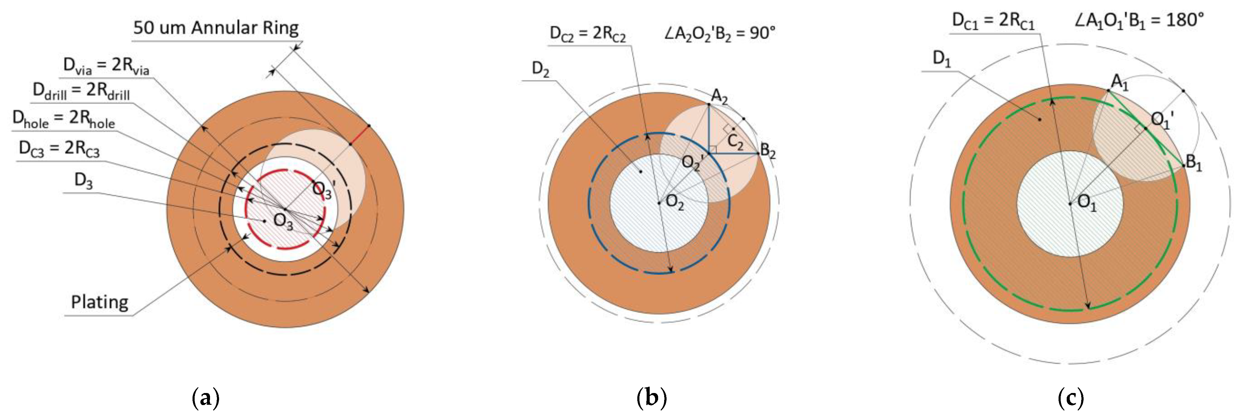
2.1. Determination of Via Requirements

The standards IPC-6012B [16] and IPC-A-600G [17] define different reliability classes for PCBs: class 3 for aerospace electronics, class 2 for industrial equipment, and class 1 for consumer equipment. The reliability class of the device should be determined before its design based on the technical requirements and intended operating conditions. Each class has different requirements. The requirements of standards for supported holes are chosen as the basis for forming the criteria for assessing the acceptability of the vias [17]:
  • Class 3: “Holes are not centered in the lands, but annular ring measures 0.05 mm or more”;
  • Class 2: “90° breakout or less”;
  • Class 1: “180° breakout or less”.
The presented limitations are difficult to use to assess the possibility of manufacturing an acceptable PCB. Therefore, based on the requirements, we will determine the numerical value of the permissible offset of the hole center relative to the center of the contact pad (Figure 2).
  • D v i a —diameter of the via or plated through-hole pad;
  • D d r i l l —diameter of the drilled hole;
  • D h o l e —diameter of the drilled hole with plating;
  • D 3 , D 2 , D 1 —areas of permissible hole center offset for the corresponding reliability classes;
  • D C 3 , D C 2 , D C 1 —diameters of the permissible hole center misalignment area for the corresponding reliability classes.
Therefore, for PCBs to meet the requirements of reliability class 3, it is necessary that the minimum size of the annular ring is not less than 50 µm. Then, the maximum offset of the hole center R C 3 is determined by Equation (1):
R C 3 = O 3 O 3 = R v i a R h o l e + 50   µ m .
In order to meet reliability class 2 requirements, the hole is allowed to extend beyond the contact pad, but the arc of the circumference of the hole extending beyond the contact pad must be less than 90°. To determine the maximum offset of the hole center R C 2 , we consider triangle O 2 A 2 B 2 : by the requirements, A 2 O 2 B 2 is straight and its sides O 2 A 2 = O 2 B 2 = R h o l e . Then, O 2 C 2 = A 2 C 2 = R h o l e 2 and angles A 2 C 2 O 2 , A 2 C 2 O 2 are straight. Now, we consider triangle O 2 A 2 C 2 : because A 2 C 2 O 2 is straight, the maximum offset of the hole center R C 2 is determined by Equation (2):
R C 2 = O 2 O 2 = O 2 A 2 2 A 2 C 2 2 O 2 C 2 = R v i a 2 R h o l e 2 2 R h o l e 2 .
The requirements of reliability class 1 are similar to those of class 2, but allow for an arc of less than 180°. Similar to the previous cases, the maximum offset of the hole center is determined relative to the center of the contact pad. In triangle O 1 A 1 B 1 , O 1 A 1 = O 1 B 1 = R v i a and A 1 O 1 = B 1 O 1 = R h o l e . Then, O 1 O 1 is the height of triangle O 1 A 1 B 1 , and A 1 O 1 O 1 is straight. Therefore, the maximum offset of the hole center R C 1 is determined by Equation (3):
R C 1 = O 1 O 1 = O 1 A 1 2 A 1 O 1 2 = R v i a 2 R h o l e 2
Thus, the probability of compliance of the manufactured contact pad with a certain reliability class can be interpreted as the probability of falling inside the area of permissible offset of the hole center D during drilling.

2.2. Formalization of the Drilling Process Using Elements of Probability Theory

Consider the drilling process, the accuracy of which is mainly determined by the accuracy of the numerically controlled machine (CNC). In this case, there is a law of distribution of random variables in the plane. To determine the type of distribution law, we introduce additional assumptions and restrictions (Figure 3a):
  • The distribution law contains two independent components X and Y , which are directed along the movement directions of the spindle on the coordinate table (Figure 3b) and obey the normal distribution law, i.e., f x = f x N ( m x , σ x ) , f y = f y N ( m y , σ y ) ;
  • The mathematical expectations of the distribution laws f x and f y are 0 and coincide with the center of the contact site: m x = m y = 0 ;
  • The standard deviations of the distribution laws are equal to each other: σ x = σ y = σ .
Thus, the distribution density function of the system of random variables f x , y will take the form (4), and the probability of hitting the hole center in the area of acceptable offset of the hole center relative to the center of the contact pad D will be determined by Equation (5) [18].
f x , y = f x y = 1 2 π σ 2 exp x 2 + y 2 2 σ 2
P X , Y D = 1 2 π σ 2 ( D ) exp x 2 + y 2 2 σ 2 d x d y
Because the area D is a circle, it is reasonable to switch from the rectangular coordinate system to the polar coordinate system. The Jacobian of the transformation is equal to r (6). Then, the density function and probability will be determined by Equations (7) and (8), respectively.
x = r cos φ y = r sin φ
f r = 1 2 π σ 2 exp r 2 2 σ 2
P X , Y D = 1 2 π σ 2 0 2 π 0 R C r exp r 2 2 σ 2 d r d φ = 1 exp R C 2 2 σ 2

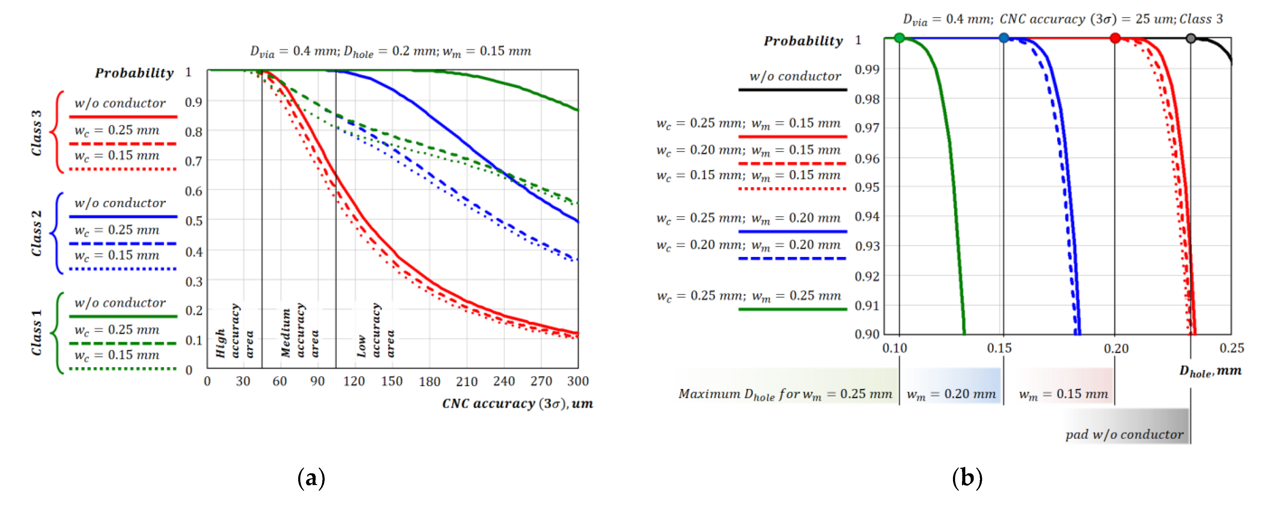
2.3. Investigation of Probability Curves for Manufacturing an Acceptable Contact Pad

Using Equation (8), we obtained curves that show the probability of manufacturing an acceptable contact pad, depending on the CNC machine accuracy and the diameter of the hole (Figure 4). We used the computer algebra system Mathcad 15 to verify mathematical expressions and to plot graphs. By the accuracy of the CNC machine, we mean the maximum value of deviation of coordinates of the input hole from the set by the program, which is equal to 3 σ . In the example we based on the manufacturing capabilities of the printed circuit board manufacturer JLCPCB [19], D v i a is 0.4 mm and D h o l e is 0.2 mm. Furthermore, in the example, the accuracy parameter is taken from a Bungard CCD CNC machine ( 3 σ = 25   µ m ) [20].
On the precision side of the CNC machine, it can be seen (Figure 4a) that reducing the reliability class will have little effect on contact pad manufacturing, as existing modern systems have a precision of about 25 µm or less, and significant differences begin at a lower precision than this value.
On the other hand, from the graph of the dependence of the probability on the hole diameter (Figure 4b), we can say that a given reliability class, as well as the size of the contact pad, largely affect the probability of acceptable manufacturing. The reliability class determines the slope of the characteristic, while the diameter of the contact pad determines the bias. In this case, the bias between the results of different classes with the same diameter is due to the need for a 50 µm annular ring for reliability class 3.
The presented dependencies describe an abstract element as a nonfunctional contact pad [8], as they consider only the contact pad to which no conductor is connected. However, the location where the contact pad is connected to the conductor can significantly reduce the reliability of a PCB when the hole is shifted to that side. It determines the importance of considering in the model (8) the influence of the conductor on the probability of manufacturing a standard-compliant result.

3. Results

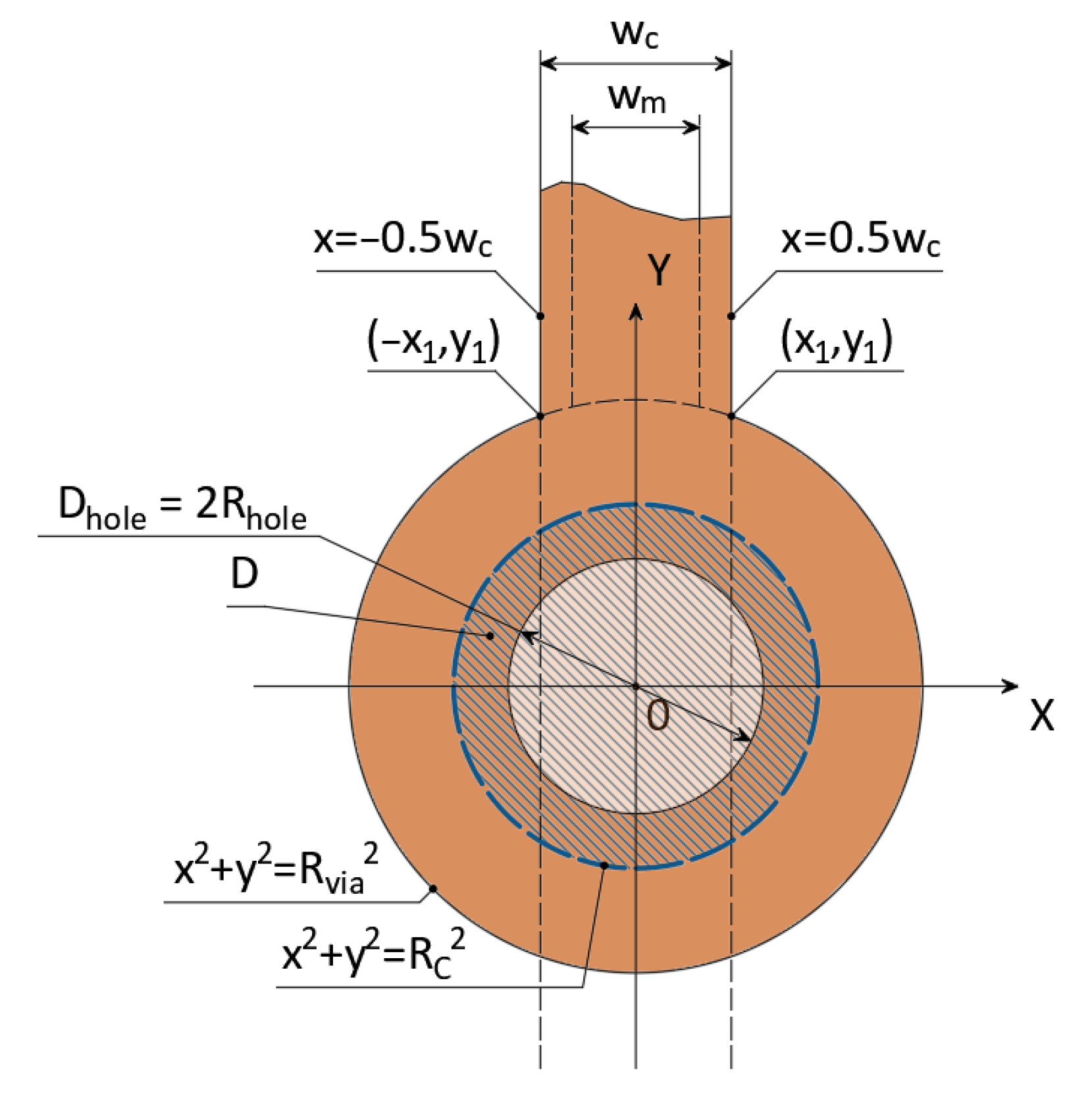
3.1. Functional Description of the Contact Pad with a Connected Conductor

Let us consider a contact pad with a conductor connected to it from the upper side (Figure 5). We introduce an additional restriction: the conductor is connected to the center of the contact pad without horizontal displacement, i.e., the figure is symmetrical along the O Y axis.
  • R v i a —radius of the via or plated through-hole pad;
  • R h o l e —radius of the drilled hole with plating;
  • R C —radius of permissible hole center offset (boundary line of the D area, depending on the selected reliability class);
  • w c —conductor width;
  • w m —minimum allowable conductor width.
We determine the points ± x 1 , y 1 of the intersection of the contact pad and the conductor. As a result, we obtain the coordinates x 1 = 0.5 w c and y 1 = R v i a 2 0.25 w c 2 . Furthermore, from the y 1 solution of the system follows the restriction on the radius of the pad: R v i a 0.5 w c .

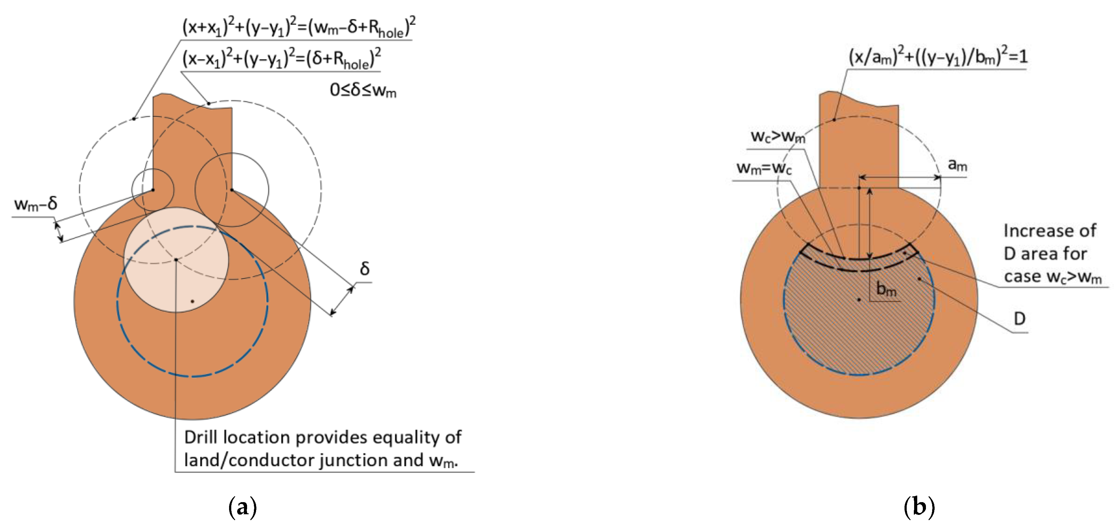
3.2. Determination of the Permissible Offset Area of a Hole with a Connected Conductor

To determine the probability of manufacturing a pad with a conductor, it is necessary to consider an additional requirement of the standard [16]: conductor-to-land-junction area should not be less than 80% of the minimum conductor width w m for PCBs of the reliability classes 3 and 2, and 70% for the class 1. For simplicity, we will further consider that the conductor-to-land-junction area should not be less than 100% of the minimum conductor width w m . This simplification should not affect the overall appearance of the resulting model. In any case, to account for this condition, we can completely replace the minimum conductor width w m with k w m , where k is the coefficient of permissible conductor width reduction (0.8 for class 3, 0.7 for classes 2 and 1).
To provide a given requirement, it is necessary to determine the boundary curve on which the center of the hole can be placed. To do this, we find partial solutions on the basis of which we build a general one. We assume that the conductor width w c is equal to the minimum conductor width w m given in the design. One solution is the symmetrical case (Figure 6a), where a conductor with a width of 0.5 w c remains to the left and right of the hole. This case corresponds to the lower intersection of circles with radius 0.5 w c + R h o l e and centers at points ± x 1 , y 1 or solution of the system of Equation (9). Let us extend the case to the general one (Figure 6b): for this purpose, we take the left circle with radius δ + R h o l e and the right one with radius w c δ + R h o l e with limits on parameter δ : 0 δ w c . Then, the system (9) will take the form (10).
y = y 1 0.5 w c + R h o l e 2 x + x 1 2 y = y 1 0.5 w c + R h o l e 2 x x 1 2
y = y 1 δ + R h o l e 2 x + x 1 2 y = y 1 w c δ + R h o l e 2 x x 1 2 , 0 δ w c
The solution of the system of Equation (10) can be represented as the lower half of an ellipse described by Equation (11). The conclusion of the equation of the ellipse and the values of its semi-axes is described in Appendix A.
x 2 a c 2 + y y 1 2 b c 2 = 1 ;   a c = 0.5 w c + R h o l e ;   b c = R h o l e ( R h o l e + w c ) ; y < y 1 .
Then, the offset area D of the hole will have the form shown in Figure 7 and consist of parts of a circle with radius R C (Figure 5) and an ellipse (11) with semi-axes a c and b c . The Figure 7 allows visual estimation of the reduction in the D area due to the connection of the conductor to the contact pad.
However, it is not always the case that the tracing of a PCB is performed by traces of the minimum permissible width. We use a similar approach to determine the curve bounding the offset area of the hole, considering the conductor, provided that the conductor width w c is greater than w m . To do this, it is necessary to determine the lower intersection of the circles with radii δ + R h o l e , w m δ + R h o l e and with centers in points ± x 1 , y 1 (Figure 8a).
In this case, the system of Equation (10) is transformed to the form (12), and the solution of the system will be defined by formula (13). The derivation of the equation of the ellipse and the values of its semi-axes is described in Appendix B. In this case, the case w c = w m can be considered as a boundary. Given this condition, the solution (17) transforms to (15), corresponding to the maximum area of the ellipse and the maximum constraint on the area D (Figure 8b).
y = y 1 δ + R h o l e 2 x + x 1 2 y = y 1 w m δ + R h o l e 2 x x 1 2 , 0 δ w m
x 2 a m 2 + y y 1 2 b m 2 = 1 ;   a m = 0.5 w m + R h o l e ;   b c = 2 R h o l e + w m 2 w c 2 2 ; y < y 1
Based on the resulting equations of circle with radius R C (Figure 5) and ellipse (13) limiting the area D in conductor-to-land-junction area, we form the integration limits for calculating the probability of producing an acceptable contact pad. Because, according to the IPC-A-600G standard [17], the conductor-to-land-junction area is a 90° sector of the contact pad located near the conductor, we introduce an additional restriction on the size of the ellipse (13): it must not contain the center of the contact site, i.e., b m y 1 . Then, the area D in the 3rd and 4th quadrants of the coordinate plane will not change, which allows us further to consider only the 1st and 2nd quadrants. Additionally, because of the symmetry of the figure vertically with respect to the axis O Y , we will further consider only the first quadrant (Figure 9a).
To determine the change in area D , it is necessary to find the intersection of ellipse (13) and a circle with varying radius r and center matching the center of the pad. It is described by the system of equations (14). The solution to the system of equations (18) is a point x 2 r , y 2 r , moving along the ellipse (13), depending on the parameter r (Figure 9a). Knowing the coordinates of this point, we can determine the dependence of the angle on the position vector φ r (Figure 9b), which determines the upper limit of integration of D area.
x 2 + y 2 = r 2 x 2 a m 2 + y y 1 2 b m 2 = 1 , y 1 b m r R C
The partial solution of the system (14) describing the lower right intersection of the circle and the ellipse is defined by Equation (15):
y 2 r = a m 2 y 1 b m a m 2 a m 2 b m 2 + y 1 2 r 2 a m 2 b m 2 a m 2 b m 2 x 2 r = r 2 y 2 2 r , y 1 b m r R C
It is also necessary to determine the value of the function φ r in the limits: r < y 1 b m . Because, in this case, the entire sector from 0 to π 2 is included in area D , φ r < y 1 b m = π 2 . Then, the dependence φ r will be determined by Equation (16). The expression of the function φ r is described in Appendix C.
φ r = arctan y 2 r x 2 r , y 1 b m r R C π 2 , r < y 1 b m
Now, the probability of hitting the center of the hole in area D will consist of the probability of hitting the lower half of the circle R C , which is equivalent to half the probability obtained by Equation (8) and twice the probability of hitting the area bounded by the function φ r , which is defined by Equation (17):
P X , Y D = 1 2 1 exp R C 2 2 σ 2 + 2 1 2 π σ 2 0 R C 0 φ r r exp r 2 2 σ 2 d φ d r = = 1 2 1 exp R C 2 2 σ 2 + 1 π σ 2 0 R C φ r r exp r 2 2 σ 2 d r

3.3. Modeling a Contact Pad with a Connected Conductor

Based on Equation (17), we plot the curves describing the probability of manufacturing a pad that complies with the standard depending on the diameter of the hole (Figure 10), or it is equivalent to increasing the diameter of the contact pad while maintaining the diameter of the hole. From the graph, we can conclude that the connection of the conductor significantly reduces the allowable hole diameter for all reliability classes. Thus, the reduction in requirements for PCBs of the reliability classes 2 and 1 relative to class 3 becomes negligible (the requirements of the classes 1 and 2 are almost equivalent to the class 3). From the illustrated example, it can be seen that the addition of a conductor limits the maximum hole diameter to 0.2 mm (0.4 mm via diameter) for all reliability classes.
Let us evaluate the effect of CNC machine precision and conductor parameters on the probability of producing a standard-compliant pad (Figure 11). Because in both cases the type of characteristic will be influenced by a large number of contact pad parameters, we will highlight common properties.
From the side of the influence of the CNC machine accuracy on the probability, the following conclusions can be made (Figure 11a):
  • In the high-precision section (up to 45 µm), the probability is independent of the reliability class.
  • At the section with medium accuracy (from 45 to 105 µm), the differences between the curves begin. The probability for the class 1 and 2 boards is higher than for the class 3 boards, but between them, their probability is almost the same. This suggests that the area D is large enough to significantly reduce the probability of acceptable manufacturing.
  • At the low-precision section (from 105 µm), the difference between the reliability classes 1 and 2 becomes significant. At this section, conductor-to-land-junction area has already influenced the resulting probability and the behavior of the curves becomes similar to the case of a nonfunctional contact pad, i.e., the probability is mainly determined by the size of the pad.
From the influence of the conductor parameters (Figure 11b), we can see that increasing the required minimum conductor width w m significantly reduces the probability of making a good contact pad, and increasing the conductor width w c relative to the minimum w m increases the slope of the curves.
Thus, the resulting model (17) allows us to analytically determine the probability of manufacturing a contact pad corresponding to a given reliability class, depending on the design parameters of the PCB: the width of the conductor (minimum acceptable w m and used w c ), hole diameter D h o l e , and the diameter of the pad D v i a . It also takes into account the peculiarities of the manufacturing process, described by the accuracy of the drilling operation.

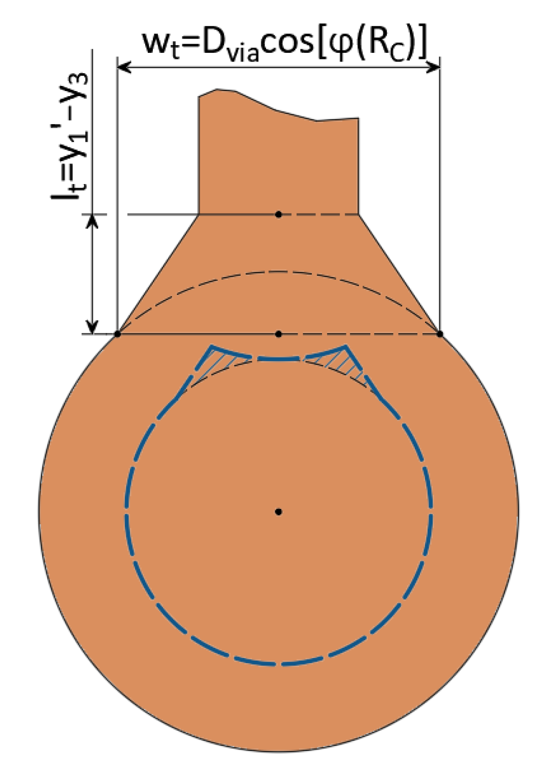
3.4. Algorithm for Determining the Parameters of a Teardrop

To ensure that the designed layout complies with the standards, it is possible to use teardrop-shaped contact pads, which have an extension at conductor-to-land-junction area, and they are actively used now. However, there are currently no rules for the design of teardrops. On the one hand, a teardrop that is too large will take up a lot of trace space. On the other hand, too small a teardrop will not yield a positive effect. Let us form the following criterion for an optimal teardrop for contact pad: the probability of manufacturing a pad with teardrop should be equal to the probability of manufacturing a contact pad without a conductor connected to it. To make the pad with teardrop comply with the formed criterion, the following algorithm is proposed (Figure 12).
The algorithm consists of the following steps:
  • Vertical displacement of the ellipse bounding the area D , so that it intersects with the circle R C at only one point 0 , R C (Figure 12a). Then, the center of the ellipse must have the coordinates 0 , R C + b m = 0 , y 1 .
  • Determining the points on the conductor and the contact pad through which the teardrop’s line will pass (Figure 12b). The first point lying on the line of the conductor must belong to the horizontal line y = y 1 , because, given the displacement of the ellipse, this line is the boundary between the conductor and the contact pad. That is, the first point has coordinates x 1 , y 1 . We define the second point as the intersection point of the circle R v i a and the line passing through the center of the coordinates and the intersection point of the circle R C and the ellipse centered at 0 , y 1 . That is, the second point will have the coordinates R v i a cos φ R C , R v i a sin φ R C = x 3 , y 3 .
  • Definition of the equation of the line f 1 x (18) forming the drop, as well as the line f 2 x closing the area D (Figure 12c). Let us introduce the assumption that the latter line is also a line (19), which is parallel to line f 1 x (18) and passes through point x 3 , y 3 = R C cos φ R C , R C sin φ R C of the intersection of the circle R C and the ellipse with center at 0 , y 1 . In reality, this is true only for the class 3 reliability, and when forming this line for the classes 2 and 1, it is necessary to use the conditions of the IPC-A-600G standard [17], which were described earlier. However, this would complicate the appearance of the curve, while insignificantly changing the D area. It can be assumed that the straight line is a stricter criterion for limiting the area D , because the arc of the hole that extends beyond the contact area will always be smaller than the reliability class specified.
f 1 x = x 3 x 1 y 3 y 1 x + y 1 x 1 x 3 x 1 y 3 y 1
f 2 x = x 3 x 1 y 3 y 1 x + y 3 x 3 x 3 x 1 y 3 y 1
Thus, the resulting teardrop shape should provide the same or higher probability of acceptable fabrication compared to no conductor connection (Figure 13). Sections that extend D farther than the circle of radius R C will not contribute significantly to the increase in probability because of the shape of the density function of the distribution law. On the other hand, excluding these areas requires the construction of a more complex teardrop shape. Therefore, given the small size of the areas, we can neglect them and assume that the contact site satisfies the optimality condition formed above.
Let us define the parameters of the teardrop, with which it can be more conveniently described. For example, the computer-aided design (CAD) system Altium Designer [21] uses its length and width as a percentage of the pad diameter D v i a (Figure 13). Then, the absolute and relative parameters of the teardrop will be determined by Equations (20) and (21), respectively.
l t = y 1 y 3 w t = D v i a c o s φ R C
l t = y 1 y 3 D v i a 100 % w t = c o s φ R C 100 %

3.5. Evaluating the Impact of Teardrop on Contact Pad

We determine the teardrop parameters for the above-described example [19] (Figure 14): contact pad diameter is 0.4 mm; transition hole diameter is 0.2 mm; minimum conductor width is 0.15 mm; conductor width is w c 0.15 ; 0.2 ; 0.25 mm (Table 1, obtained relative values of teardrop parameters rounded to accuracy 1%).
Now, let us determine the effect of the teardrop on the CNC machine’s accuracy characteristics required for acceptable manufacturing. The accuracy of the CNC machine must ensure the probability of hitting within the area of acceptable hole offset D above 0.997 (according to the 3-sigma rule). Firstly, we determine the required precision of the CNC machine for a contact pad without a teardrop. To do this, from the graph (Figure 11a), we determine the lower limit of the allowable machine accuracy, at which the probability of acceptable manufacturing is equal to 0.997. Secondly, according to the proposed algorithm for designing a teardrop, the probability of making pad with teardrop will be no less than the probability of making a contact pad without a conductor connected to it. Then, the probability of acceptable manufacturing for a contact pad with teardrop can be determined from the results shown in graph (Figure 4a). The results are presented in Table 2 below.
From the results (Table 2), it can be seen that the contact pad with teardrop allows a significant reduction in the requirements for PCB drilling equipment. Thus, the size of the allowable hole offset for devices of class 3 will increase from 20% to 50%; for class 2, from 175% to 240%; and for class 1, from 310% to 406%.

4. Discussion

The developed model has a lot of limitations and assumptions, the analysis of which will make it possible to determine the issues of model development that need to be solved:
  • Limitations of the distribution law: in the work, it is assumed that the mathematical expectation is 0, and the standard deviation of hole drilling is considered constant σ x = σ y = σ and depends only on the accuracy parameter of hole drilling, which is declared by the manufacturer in the machine documentation. However, in reality, these characteristics are more difficult to determine. For example, the mathematical expectation will depend on the coordinates of the hole (with increasing distance from the origin of coordinates, error can accumulate) and also possible change in parameters during operation due to wear of equipment.
  • From the manufacturing point of view, the model needs to be extended, because currently, it takes into account only the influence of the drilling operation. For example, during the PCB manufacturing process, etching of conductors inevitably results in lateral subtraction of the conductors, which will reduce the size of the contact pad and the size of the area of permissible hole offset D [22]. In addition, the model does not consider displacement of the layers of the PCB caused by deformation during their manufacturing.

5. Conclusions

At present, the obtained model shows the opportunity to determine the probability of manufacturing an acceptable contact pad according to the given design parameters and manufacturing process specifications, i.e., it is a quantitative criterion for evaluating the quality of a PCB. However, it also allows us to solve the opposite problem: determining the design parameters for a given probability and the characteristics of the manufacturing process or determining the necessary production line for the manufacture of an electronic device.
Furthermore, the need for modernization of PCB CAD systems has been identified, namely, adding the ability to create separate classes for teardrops, which is currently missing (for example, in Altium Designer CAD, all drop contact pads are defined by one rule). It is necessary because the parameters of a drop contact pad depend on topology parameters, which can differ greatly within the same PCB (e.g., for signal and power traces). The addition of separate teardrop classes will increase the density of interconnects without compromising the reliability.
In the future, the obtained analytical model can be used as a criterion for quantitative assessment of printed circuit board quality, and its use in the development process will allow defining necessary parameters of PCB design depending on manufacturing parameters of drilling operation and device reliability class.
Now, we can highlight two main issues for the development of this work. The first issue is related to the generalization of the proposed method of reliability estimation to form an algorithm for creating similar probabilistic models for other stages of the PCB manufacturing process. This would simplify the process of expanding the model to take into account new parameters (displacement and deformation of layers in multilayer PCBs, subtraction of the conductive pattern, etc.) and eventually allow forming a general model for assessing the reliability of printed circuit boards depending on their design parameters and manufacturing production process. The second direction is related to the development of a software product for automatic calculation of reliability and its integration with modern CAD systems for PCBs. This tool would provide the designer with additional feedback for evaluating the reliability of a PCB and would allow evaluating in advance the possibility of manufacturing it at a particular production facility.

Author Contributions

Conceptualization, M.A.K.; methodology, F.V.V.; software, M.A.K.; validation, F.V.V. and O.V.K.; formal analysis, M.A.K.; investigation, M.A.K.; resources, O.V.K.; data curation, O.V.K.; writing—original draft preparation, M.A.K.; writing—review and editing, F.V.V. and O.V.K.; visualization, M.A.K. and O.V.K.; supervision, F.V.V.; project administration, F.V.V.; funding acquisition, O.V.K. All authors have read and agreed to the published version of the manuscript.

Funding

The work was supported by the Russian science Foundation, grant No. 23-29-10204.

Data Availability Statement

Data are contained within the article.

Conflicts of Interest

The authors declare no conflict of interest.

Appendix A. Determining the Equation of the Curve Limiting the Permissible Offset of the Hole Center Relative to the Center of the Pad in the Conductor-to-Land-Junction Area for the Case Where the Conductor Width Is Equal to the Minimum Possible

To determine the type of curve limiting the acceptable offset of the hole center relative to the center of the contact pad in the conductor-to-land-junction area for the case of equality of the conductor width to the minimum possible, it is necessary to solve the system of Equation (A1):
y = y 1 δ + R h o l e 2 x + x 1 2 y = y 1 w c δ + R h o l e 2 x x 1 2 , 0 δ w c .
Both equations in the system (A1) are expressed relative to y . Equate their right-hand sides to each other, square them, and substitute x 1 = 0.5 w c (A2):
δ + R h o l e 2 x + 0.5 w c 2 = w c δ + R h o l e 2 x 0.5 w c 2 .
Divide the summands with and without the variable x (A3):
w c δ + R h o l e 2 δ + R h o l e 2 = x 0.5 w c 2 x + 0.5 w c 2 .
Expand the difference squares in both parts of the equation, and express the function x δ (A4):
w c δ + R h o l e + δ + R h o l e w c δ + R h o l e δ R h o l e = = x 0.5 w c + x + 0.5 w c x 0.5 w c x 0.5 w c , w c + 2 R h o l e w c 2 δ = 2 x w c , w c w c + 2 R h o l e 2 w c 2 δ w c + 2 R h o l e 2 w c = x , x δ = w c + 2 R h o l e w c δ w c + 2 R h o l e 2 .
Find the definition area of the function x δ (A5):
w c + 2 R h o l e 2 x w c + 2 R h o l e 2 .
Substitute the resulting function x δ into one in the original Equation (A1), and obtain the result (A6):
y = y 1 δ + R h o l e 2 x δ + w c 2 2 .
Consider separately the expression under the square root of the function (A6), and transform it to the form (A7):
δ + R h o l e 2 x δ + w c 2 2 = δ + R h o l e + x δ + w c 2 δ + R h o l e x δ w c 2 = = x δ = w c + 2 R h o l e w c δ w c + 2 R h o l e 2 = = δ + R d r i l l + w c + 2 R h o l e w c δ w c + 2 R h o l e 2 + w c 2 δ + R d r i l l w c + 2 R h o l e w c δ + w c + 2 R h o l e 2 w c 2 = = δ + R h o l e + δ + 2 R h o l e w c δ w c 2 R h o l e + w c 2 δ + R h o l e δ 2 R h o l e w c δ + w c 2 + R h o l e w c 2 = = 2 δ + 2 R h o l e w c δ 2 R d r i l l 2 R h o l e w c δ = 4 R h o l e δ 1 + R h o l e w c 1 δ w c .
Thus, the solution of the system (A1) in the parametric form (A8) can be derived:
x δ = w c + 2 R h o l e w c δ w c + 2 R h o l e 2 y δ = y 1 2 R h o l e δ 1 + R h o l e w c 1 δ w c , 0 δ w c .
From Equation (A4), the dependence δ x is found (A9):
δ x = w c w c + 2 R h o l e x + w c 2 .
Substitute δ x into one of the equations of system (A1) to obtain Equation (A10):
y = y 1 δ x + R h o l e 2 x + w c 2 2 .
Consider separately the expression under root of Equation (A10), and transform it to the form (A11):
δ x + R h o l e 2 x + w c 2 2 = δ x + R h o l e + x + w c 2 δ x + R h o l e x w c 2 = δ x = w c x w c + 2 R h o l e + w c 2 = = w c x w c + 2 R h o l e + w c 2 + 2 R h o l e + x + w c 2 w c x w c + 2 R h o l e + w c 2 + R h o l e x w c 2 = = w c x w c + 2 R h o l e + w c + 2 R h o l e + x w c x w c + 2 R h o l e + R h o l e x = = w c x w c + 2 R h o l e 2 + R h o l e w c x w c + 2 R h o l e w c x 2 w c + 2 R h o l e + w c 2 x w c + 2 R h o l e + w c R h o l e w c x + + R h o l e w c x w c + 2 R d r i l l + R h o l e 2 R h o l e x + w c x 2 w c + 2 R h o l e + R h o l e x x 2 = = x 2 w c w c + 2 R h o l e 2 1 + x 2 R h o l e w c w c + 2 R h o l e + w c 2 w c + 2 R h o l e w c + w c R h o l e + R h o l e 2
Consider the coefficient at x in Equation (A11), and determine that it is zero (A12):
2 R h o l e w c w c + 2 R h o l e + w c 2 w c + 2 R h o l e w c = 2 R h o l e w c + w c 2 w c 2 2 R h o l e w c w c + 2 R h o l e = 0 .
Then, Equation (A10) will take the form (A13):
y = y 1 x 2 w c w c + 2 R h o l e 2 1 + w c R h o l e + R h o l e 2 .
Perform the following transformations (A14):
x 2 1 w c w c + 2 R h o l e 2 + y y 1 2 = w c R h o l e + R h o l e 2 x 2 w c 2 + 4 w c R h o l e + 4 R h o l e 2 w c 2 w c + 2 R h o l e 2 w c R h o l e + R h o l e 2 + y y 1 2 w c R h o l e + R h o l e 2 = 1 ; x 2 w c + 2 R h o l e 2 w c R h o l e + R h o l e 2 4 w c R h o l e + R h o l e 2 + y y 1 2 w c R h o l e + R h o l e 2 = 1 ; x 2 0.5 w c + R h o l e 2 + y y 1 2 R h o l e ( R h o l e + w c ) 2 = 1 .
Thus, the solution of the system (A1) belongs to the equation of the ellipse (A15):
x 2 a c 2 + y y 1 2 b c 2 = 1 ; a c = 0.5 w c + R h o l e ; b c = R h o l e ( R h o l e + w c ) ; w c + 2 R h o l e 2 x w c + 2 R h o l e 2 .
The obtained solution also has an additional restriction: only the lower half of the ellipse corresponds to the solution of the original system of Equation (A1). The upper half of the ellipse is not a solution, as it appeared forcedly when squaring the original equation of the system (A1).

Appendix B. Determining the Curve Equation Limiting the Acceptable Offset of the Hole Center Relative to the Center of the Contact Pad in the Conductor-to-Land-Junction Area for the Case of Inequality with the Conductor Minimum Width

To determine the type of curve limiting the acceptable offset of the hole center relative to the center of the contact pad in the conductor-to-land-junction area, it is necessary to solve the system of Equation (A16) for the case of inequality of the conductor width with the minimum possible.
y = y 1 δ + R h o l e 2 x + x 1 2 y = y 1 w m δ + R h o l e 2 x x 1 2 , 0 δ w m .
Both equations are expressed relative to y . Equate their right sides to each other, squared, and substitute x 1 = 0.5 w c (A17):
δ + R h o l e 2 x + 0.5 w c 2 = w m δ + R h o l e 2 x 0.5 w c 2 .
Divide the summands with and without the variable x (A18):
w m δ + R h o l e 2 δ + R h o l e 2 = x 0.5 w c 2 x + 0.5 w c 2 .
Expand the difference squares in both parts of the equation, and express the function δ x (A19):
w m δ + R h o l e + δ + R h o l e w m δ + R h o l e δ R h o l e = = x 0.5 w c + x + 0.5 w c x 0.5 w c x 0.5 w c ; w m + 2 R h o l e w m 2 δ = 2 x w c ; δ x = w c w m + 2 R h o l e x + w m 2 .
Also express the function x δ , and find the range of the function (A20):
x δ = w m + 2 R h o l e w m + 2 δ 2 w c = w m + 2 R h o l e w c δ w m + 2 R h o l e 2 w c w m ; w m + 2 R h o l e 2 w c w m x w m + 2 R h o l e 2 w c w m .
Substitute this function x δ into one in the original Equation (A16) to obtain expression (A21):
y = y 1 δ x + R h o l e 2 x + w c 2 2 .
Consider separately the expression under square root of Equation (A21), and obtain the following result (A22):
δ x + R h o l e 2 x + w c 2 2 = δ x + R h o l e + x + w c 2 δ + R h o l e x w c 2 = = δ x = w c w m + 2 R h o l e x + w m 2 = = w c x w m + 2 R h o l e + w m 2 + R h o l e + x + w c 2 w c x w m + 2 R h o l e + w m 2 + R h o l e x w c 2 = = w c w m + 2 R h o l e + 1 x + R h o l e + w c 2 + w m 2 w c w m + 2 R h o l e 1 x + R h o l e w c 2 + w m 2 .
Perform substitutions (A23):
a = w c w m + 2 R h o l e + 1 ; b = R h o l e + w c 2 + w m 2 ; c = w c w m + 2 R h o l e 1 ; d = R h o l e w c 2 + w m 2 .
Then, expression (A22) will take the form (A24):
w c w m + 2 R h o l e + 1 x + R h o l e + w c 2 + w m 2 w c w m + 2 R h o l e 1 x + R h o l e w c 2 + w m 2 = = a x + b c x + d = a c x 2 + a d + b c x + b d .
Determine the components at powers of x (A25):
a c = w c w m + 2 R h o l e + 1 w c w m + 2 R h o l e 1 = w c 2 2 R h o l e + w m 2 1 ; a d = w c w m + 2 R h o l e + 1 R h o l e w c 2 + w m 2 = w c R h o l e 0.5 w c 2 + 0.5 w c w m w m + 2 R h o l e + R h o l e w c 2 + w m 2 ; c b = w c w m + 2 R h o l e 1 R h o l e + w c 2 + w m 2 = w c R h o l e + 0.5 w c 2 + 0.5 w c w m w m + 2 R h o l e R h o l e w c 2 w m 2 ; a d + c b = w c R h o l e 0.5 w c 2 + 0.5 w c w m + w c R h o l e + 0.5 w c 2 + 0.5 w c w m w m + 2 R h o l e + R h o l e w c 2 + w m 2 R h o l e w c 2 w m 2 = = 2 w c R h o l e + w c w m w m + 2 R h o l e w c = 2 w c R h o l e + w c w m w c w m 2 w c R h o l e w m + 2 R h o l e = 0 ; b d = R h o l e + w c 2 + w m 2 R h o l e w c 2 + w m 2 = = R h o l e 2 R h o l e w c 2 + R h o l e w m 2 + R h o l e w c 2 w c 2 4 + w c w m 4 + R h o l e w m 2 w c w m 4 + w m 2 4 = = 4 R h o l e 2 + 4 R h o l e w m + w m 2 w c 2 4 = 2 R h o l e + w m 2 w c 2 4 .
Then, the original expression (A24) can be represented as an ellipse with semi-axes a m and b m (A26):
y y 1 2 = a c x 2 + b d ; a c b d x 2 + y y 1 2 b d = 1 ; x 2 a m 2 + y y 1 2 b m 2 = 1 ; w m + 2 R h o l e 2 w c w m x w m + 2 R h o l e 2 w c w m ; a m = b d a c = 2 R h o l e + w m 2 w c 2 4 ÷ w c 2 2 R h o l e + w m 2 1 = = 2 R h o l e + w m 2 w c 2 2 R h o l e + w m 2 4 w c 2 2 R h o l e + w m 2 = 2 R h o l e + w m 2 ; b m = b d = 2 R h o l e + w m 2 w c 2 4 = 2 R h o l e + w m 2 w c 2 2 .
Similarly to the case considered in Appendix A, the solution of the original system (A16) is satisfied only by the lower half of the ellipse.

Appendix C. Derivation of the Function Limiting the Integration Area When Considering the “Conductor—Contact Pad” System

In order to determine the function limiting the integration region D , it is necessary to solve the system of Equation (A27):
x 2 + y 2 = r 2 x 2 a m 2 + y y 1 2 b m 2 = 1 , y 1 b m r R C .
Express x 2 from the upper equation of the system, and substitute it in the lower one (A28):
r 2 y 2 a m 2 + y y 1 2 b m 2 = 1 ; b m 2 r 2 b m 2 y 2 + a m 2 y 2 2 a m 2 y 1 y + a m 2 y 1 2 = a m 2 b m 2 ; a m 2 b m 2 y 2 2 a m 2 y 1 y + a m 2 y 1 2 a m 2 b m 2 + b m 2 r 2 = 0 .
Solve the resulting Equation (A29):
y r = a m 2 y 1 ± a m 4 y 1 2 a m 2 b m 2 a m 2 y 1 2 a m 2 b m 2 + b m 2 r 2 a m 2 b m 2 .
Consider separately the expression under square root in the function y r (54), and transform it to the form (A30):
a m 4 y 1 2 a m 2 b m 2 a m 2 y 1 2 a m 2 b m 2 + b m 2 r 2 = = a m 4 y 1 2 a m 4 y 1 2 a m 4 b m 2 + a m 2 b m 2 r 2 a m 2 b m 2 y 1 2 + a m 2 b m 4 b m 4 r 2 = = a m 4 b m 2 a m 2 b m 2 r 2 + a m 2 b m 2 y 1 2 a m 2 b m 4 + b m 4 r 2 = = b m 2 a m 2 a m 2 b m 2 + y 1 2 r 2 a m 2 b m 2 .
Then, y r , given that we are looking only for the lower intersection, converts to the form (A31):
y r = y 2 r = a m 2 y 1 b m a m 2 a m 2 b m 2 + y 1 2 r 2 a m 2 b m 2 a m 2 b m 2 .
Substitute the function y r into the upper equation of system (A27) to obtain x r (A32):
x r = x 2 r = r 2 y 2 2 r .
Thus, the function φ r will be equal to (A33):
φ r = arctan y 2 r x 2 r , y 1 b m r R C .

References

  1. Medvedev, A.M. Electronic components and mounting substrates. Continuous integration. Compon. Technol. 2006, 12, 124–134. [Google Scholar]
  2. Busurin, V.I.; Korobkov, K.A.; Shleenkin, L.A.; Makarenkova, N.A. Compensation Linear Acceleration Converter Based on Optical Tunneling. In Proceedings of the 2020 27th ICINS, Saint Petersburg, Russia, 25–27 May 2020; pp. 1–4. [Google Scholar] [CrossRef]
  3. Busurin, V.I.; Korobkov, V.V.; Korobkov, K.A.; Koshevarova, N.A. Micro-Opto-Electro-Mechanical System Accelerometer Based on Coarse-Fine Processing of Fabry–Perot Interferometer Signals. Meas. Tech. 2021, 63, 883–890. [Google Scholar] [CrossRef]
  4. Kim, J.; Ko, J.; Choi, H.; Kim, H. Printed Circuit Board Defect Detection Using Deep Learning via A Skip-Connected Convolutional Autoencoder. Sensors 2021, 21, 4968. [Google Scholar] [CrossRef] [PubMed]
  5. Vancov, S.; Khomutskaya, O. A method for increasing the reliability of obtaining holes in printed circuit boards. In Proceedings of the 2021 ICOECS, Ufa, Russia, 16–18 November 2021; pp. 513–515. [Google Scholar]
  6. Khomutskaya, O.; Vancov, S.; Korobkov, M.; Medvedev, A. The method of automated evaluation of the deformation of the printed circuit board. In Proceedings of the 2021 ICOECS, Ufa, Russia, 16–18 November 2021; pp. 510–512. [Google Scholar]
  7. Vantsov, S.V.; Vasil’ev, F.V.; Medvedev, A.M.; Khomutskaya, O.V. Quasi-Determinate Model of Thermal Phenomena in Drilling Laminates. Russ. Eng. Res. 2018, 38, 1074–1076. [Google Scholar] [CrossRef]
  8. Vantsov, S.V.; Vasil’ev, F.V.; Medvedev, A.M.; Khomutskaya, O.V. Influence of Nonfunctional Contact Pads on Printed-Circuit Performance. Russ. Eng. Res. 2020, 40, 442–445. [Google Scholar] [CrossRef]
  9. Vasilyev, F. Physical Reliability of Electronics; Moscow Aviation Institute (National Research University): Moscow, Russia, 2022; p. 160. [Google Scholar]
  10. Amosov, A.G.; Golikov, V.A.; Kapitonov, M.V.; Vasilyev, F.V.; Rozhdestvensky, O.K. Engineering and Analytical Method for Estimating the Parametric Reliability of Products by a Low Number of Tests. Inventions 2022, 7, 24. [Google Scholar] [CrossRef]
  11. Cherkasov, K.; Meshkov, S.; Makeev, M.; Ivanov, Y.; Shashurin, V.; Tsvetkov, Y.; Khlopov, B. Computer statistical experiment for analysis of resonant-tunneling diodes I–V characteristics. In International Scientific Conference Energy Management of Municipal Facilities and Sustainable Energy Technologies EMMFT 2018; Springer International Publishing: Cham, Switzerland, 2019; Volume 983, pp. 626–634. [Google Scholar] [CrossRef]
  12. Makeev, M.O.; Sinyakin, V.Y.; Meshkov, S.A. Reliability prediction of resonant tunneling diodes and non-linear radio signal converters based on them under influence of temperature factor and ionizing radiations. Adv. Astronaut. Sci. 2020, 170, 655–664. [Google Scholar]
  13. Makeev, M.O.; Sinyakin, V.Y.; Meshkov, S.A. Reliability prediction of radio frequency identification passive tags power supply systems based on A3B5 resonant-tunneling diodes. In Proceedings of the 2018 International Russian Automation Conference, Sochi, Russia, 9–16 September 2018; pp. 1–5. [Google Scholar] [CrossRef]
  14. Medvedev, A.; Vasilyev, F.; Sokolsky, M. Testing of hidden defects in interconnections. Amazon. Investig. 2019, 8, 746–756. [Google Scholar]
  15. Korobkov, M.; Vasilyev, F.; Mozharov, V. A Comparative Analysis of Printed Circuit Boards with Surface-Mounted and Embedded Components under Natural and Forced Convection. Micromachines 2022, 13, 634. [Google Scholar] [CrossRef] [PubMed]
  16. IPC-6012B; Qualification and Performance Specification for Rigid Printed Boards. IPC International: Bannockburn, IL, USA, 2007.
  17. IPC–A–600G; Acceptability of Printed Boards. IPC International: Bannockburn, IL, USA, 2004.
  18. Ventzel, E.S. Probability Theory, 6th ed.; Vyssh. shk.: Moscow, Russia, 1999; p. 576. [Google Scholar]
  19. PCB Manufacturing & Assembly Capabilities. Available online: https://jlcpcb.com/capabilities/pcb-capabilities (accessed on 26 February 2023).
  20. Bungard CCD/ATC Machining Center. Available online: https://www.protehnology.ru/obrabatyvaushiy-centr-bungard-elektronik-bungard-ccdatc (accessed on 7 May 2023).
  21. Teardrops. Available online: https://www.altium.com/ru/documentation/altium-designer/pcb-dlg-teardropoptionsformteardrops-ad/?version=22 (accessed on 26 February 2023).
  22. Vasilyev, F.; Isaev, V.; Korobkov, M. The influence of the PCB design and the process of their manufacturing on the possibility of a defect-free production. Prz. Elektrotechniczny 2021, 97, 91–96. [Google Scholar] [CrossRef]
Figure 1. IDEF0 top-level diagram of the proposed method of reliability assessment.
Inventions 08 00077 g001
Figure 2. Determination of the area of permissible displacement of the hole center relative to the center of the contact pad according to IPC-A-600G [17]: (a) For 3 reliability class (red area); (b) For 2 reliability class (blue area); (c) For 1 reliability class (green area).
Inventions 08 00077 g002
Figure 3. Formalization of the drilling process: (a) Probability characteristics of hitting the contact pad during drilling: red, blue and green lines correspond to the areas of permissible offset of the hole center for reliability classes 3, 2 and 1, respectively; (b) Coordinate field of a Bungard CCD CNC machine.
Inventions 08 00077 g003
Figure 4. Probability of making an acceptable contact pad: (a) Depending on the precision of the CNC machine; (b) Depending on the diameter of the hole.
Inventions 08 00077 g004
Figure 5. Design parameters of the contact pad.
Inventions 08 00077 g005
Figure 6. Figure 6. Permissible location of the hole for the case where the conductor width is equal to the minimum acceptable ( w c = w m ): (a) The hole center is located on the symmetry axis; (b) The hole center is located asymmetrically.
Inventions 08 00077 g006
Figure 7. Constraint on the offset area D of the hole, including the conductor ( w c = w m ).
Inventions 08 00077 g007
Figure 8. Permissible location of the hole for the case where the width of the conductor is greater than the minimum acceptable ( w c > w m ): (a) Particular case of the hole position; (b) Changes in the area D with relation to the case where w c = w m .
Inventions 08 00077 g008
Figure 9. Changing the area D of acceptable offset of the hole center: (a) Determining the intersection of the circle with radius R C and the ellipse (13); (b) Determining the function in the polar coordinate system.
Inventions 08 00077 g009
Figure 10. Probability of manufacturing an acceptable pad depending on the diameter of the hole, taking into account the connected conductor (overlapping curves of different reliability classes are marked in gray).
Inventions 08 00077 g010
Figure 11. Probability of making an acceptable pad considering the connected conductor: (a) Depending on the accuracy of the CNC machine; (b) Depending on the diameter of the hole.
Inventions 08 00077 g011
Figure 12. Stages of constructing a teardrop: (a) Shift of the ellipse limiting the area D ; (b) Determination of key points; (c) Drawing lines.
Inventions 08 00077 g012
Figure 13. The shape of the D area of the pad with teardrop and its construction parameters according Altium Designer CAD system [21].
Inventions 08 00077 g013
Figure 14. Construction of teardrops: solid red color indicates areas of class 3, blue—class 2, green—class 1; dashed line indicates increase in area D after changing the form of the pad.
Inventions 08 00077 g014
Table 1. Teardrop parameters.
Reliability ClassTeardrop
Parameter
Conductor   Width   w c Conductor   Width   w c Conductor   Width   w c
3Length, l t , % ( l t , mm)21 (0.08)15 (0.06)7 (0.03)
Width, w t , % ( w t , mm)78 (0.31)75 (0.30)70 (0.28)
2Length, l t , % ( l t , mm)44 (0.18)41 (0.16)35 (0.14)
Width, w t , % ( w t , mm)87 (0.35)87 (0.35)87 (0.35)
1Length, l t , % ( l t , mm)55 (0.22)52 (0.21)48 (0.19)
Width, w t , % ( w t , mm)83 (0.33)84 (0.34)85 (0.34)
Table 2. Required accuracy of the CNC machine, μm.
Reliability Class W / o   Teardrop   ( w c = 0.15 mm ) W / o   Teardrop   ( w c = 0.20 mm ) W / o   Teardrop   ( w c = 0.25 mm ) With Teardrop
330323745
2303237102
1303237152
Disclaimer/Publisher’s Note: The statements, opinions and data contained in all publications are solely those of the individual author(s) and contributor(s) and not of MDPI and/or the editor(s). MDPI and/or the editor(s) disclaim responsibility for any injury to people or property resulting from any ideas, methods, instructions or products referred to in the content.

