Communication

How to Increase the Analog-to-Digital Converter Speed in Optoelectronic Systems of the Seed Quality Rapid Analyzer

1
Computer Technologies and Information Security Faculty, Rostov State University of Economics, 69, Bolshaya Sadovaya, Rostov-on-Don 344002, Russia
2
Management Information Technology Faculty, Rostov State Transport University, 2, Rostovskogo Strelkovogo Polka Narodnogo Opolcheniya sq., Rostov-on-Don 344038, Russia
3
Mechanical Department, Voronezh State University of Forestry and Technologies named after G.F. Morozov, 8, Timiryazeva, Voronezh 394087, Russia
4
Faculty of Forestry, University of Belgrade, 1 Kneza Višeslava, 11030 Belgrade, Serbia
*
Author to whom correspondence should be addressed.
Inventions 2019, 4(4), 61; https://doi.org/10.3390/inventions4040061
Submission received: 29 August 2019 / Revised: 26 September 2019 / Accepted: 30 September 2019 / Published: 6 October 2019
(This article belongs to the Special Issue Automatic Control and System Theory)

Abstract

:
This invention is relevant when working as part of optoelectronic systems, including non-destructive quality control of forest seeds. The possibility of synthesis of the ultrafast optical analog-to-digital converter (ADC) providing conversion of analog information to digital in the sub-GHz range is considered. The functional scheme of the optical ADC, containing technologically well-developed optical elements is given; the principle of operation is described in detail. The possibility of increasing the speed of the ADC to make it potentially possible for optical data processing schemes is shown.

1. Introduction

In modern forest seed production, challenges for non-destructive seed quality control often arise [1]. Features of collection and storage of forest seeds suggest the presence of mobile Express analyzers [2]. They operate in different optical ranges, are designed on a modular basis and have the ability not only to diagnose, but also to separate [3,4] seeds by spectrometric properties [5,6,7]. The bases of these devices are optoelectronic systems [8] allowing, depending on the specific optical index of the seed, to calculate its viability [9,10,11,12,13,14,15]. The speed of any information-computing system depends to a significant extent on the speed of its interface, especially in a situation where it is used to control physical and technical processes in real time [16].
In this case, of particular importance is the speed of buffer devices that convert analog information into digital. For multi-bit converters (with the number of bits N > 10), the problem of speed information processing in the sub-GHz (and larger) range has not yet been solved. The lack of a high-speed interface negates all the advantages of any converter. To date, a very urgent task is the development of an analog-to-digital converter (ADC) with a conversion rate commensurate with the potential possible speeds of optical switching circuits.
Currently known ADCs:
  • based on the use of electronic functional elements [17],
  • ADC-based waveguide modulators of the type Mach-Zehnder [18],
  • ADC based on the use of optical bistable elements (OBEs) and distributed optical waveguides [19], etc.
The obvious disadvantages of electronic ADCs are their low speeds, which decrease even more with the growth of the ADC bit rate, and high complexity. In turn, the disadvantages of the ADC based on waveguide Mach-Zehnder type modulators [18] are the ability to convert the input analog signal only to gray code (and not the positional binary code) and the overall low performance of the ADC due to the need to use a large number of electronic elements (photodetectors, amplifiers, comparator, etc.) in the terminal cascade with a total response time ≥ 10−6 s. Such a short response time does not allow to process information in the sub-GHz range.
Among the listed ADC, the fastest is the ADC based on waveguide optical elements [19], but in this ADC the conversion time is directly proportional to its output code and the pulse repetition period. Since this ADC operates in a cyclic mode (at the end of the conversion time interval, the counter is set to the initial state and therefore the conversion always starts from zero), its disadvantage is that it does not have a very high speed, which does not allow analog-to-digital conversion in the sub-GHz range.
Let us consider further the possibility of synthesis of optical ADC, which provides conversion into positional binary code of electrical analog signals in control and communication systems, information processing in which is carried out in sub-GHz and large ranges.

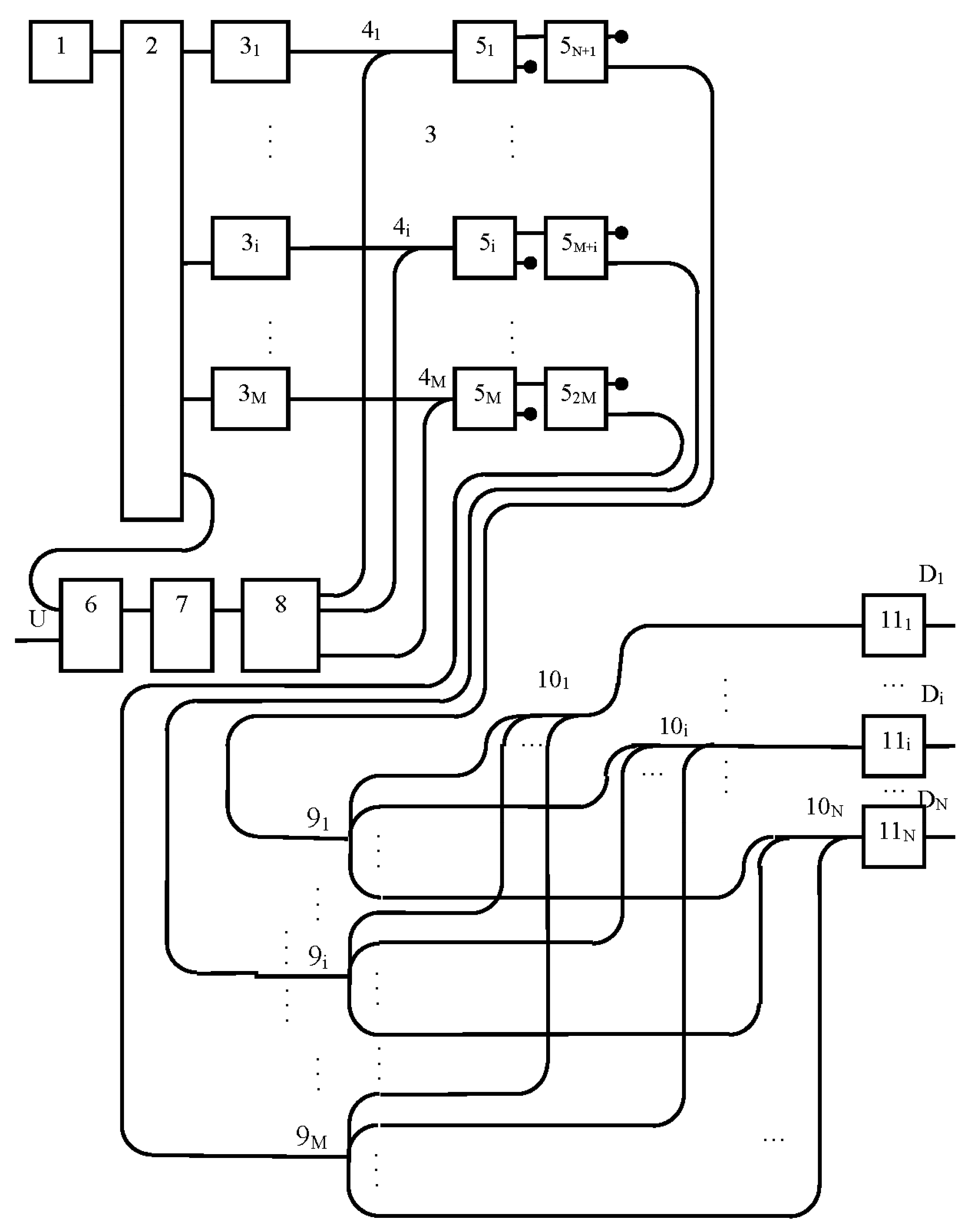
2. The Optical ADC Principle

The functional scheme of the considered optical ADC, focused on the possibility of integrated optical performance [18,20], is shown in Figure 1.
N-bit optical ADC contains a coherent radiation source 1, K-output optical splitter 2 (K = M + 1, M = 2N − 1, N—number of ADC discharges), M optical transparencies 3i (i = 1…M), M optical Y-unifiers 4i, two groups of M OBEs in each 5i and 5M+i, electro-optical amplitude modulator 6, optical phase modulator 7, M-output optical splitter 8, M N-output optical splitters 9i, N M-input optical unifiers 10j, and N photodetectors 11j (j = 1…N).
It should be noted that a significant number of optical splitters that are part of this ADC lead to strict requirements for their manufacturing, providing a maximum relative error of signal transmission, which in assessing the accuracy of the ADC can be neglected, of no more than 0.001%. To date, a similar level of technology for the production of optical splitters has been achieved by Michael S. Cohen (Qikertown, PA, USA) and Nanonics Imaging Ltd. (Jerusalem, Israel); splitters that have insertion loss less than 0.1 dB, flatness ratio offshoots 0.1 dB, back reflection less than −60 dB. When using optical splitters with less qualitative characteristics, correction of signal distortions can be carried out, for example, due to a corresponding change in the transmission coefficients of optical transparencies 3i (see Figure 1).
OBEs 5i (i = 1…2M) are optical elements that transmit an optical signal from the input to the first (direct) output, if the amplitude of the input optical signal is greater than or equal to the specified threshold value. Otherwise, the optical signal is transmitted to the second (inverse) output. OBEs may be made in the form of optical transistors [20], optically connected waveguides [18,20,21] and others [22,23].
The OBE threshold of the first group 5i (i = 1…M) is equal to N − 1/2M conventional units, and the threshold of OBEs of the second group 5M+i is equal to N + 1/2M conventional units. The light-absorbing outputs are the second (inverse) OBEs outputs of the first group, 5i, and the first (direct) OBEs outputs of the second group, 5M+i. The input of the optical ADC U is the control input of electro-optical amplitude modulator 6.
The scheme of connection of the functional elements of the optical ADC is shown in Figure 1; it should be noted that the outputs from the first to the M-th K-output optical splitter 2 are connected to the inputs of optical banners 31…3M, and (M + 1)-th. The output of optical splitter 2 is connected to the information input of electro-optical amplitude modulator 6.
A feature of the optical scheme of this ADC is also that the outputs of N-output optical splitters 9i are connected to the inputs of M-input optical unifiers 10j (j = 1…N) in such a way that in the presence of an optical signal at the input of i-th N-output optical splitter 9i, a positional binary code of the number “i” is formed at all N outputs of M-input optical splitters 10j. At the same time, some optical branching of N-output optical splitters 9i are light-absorbing or do not absorb light waves. This process is explained by the presence/absence of appropriate connections between the optical splits of N-output optical splitters 9i and the optical branches of M-input optical splitters 10j. The outputs of the M-input optical unifiers 10j are already optically connected to the inputs of the same-name photodetectors 11j, the outputs of which “D1…DN” are the outputs of the ADC.
Each optical splitter 9i has a number of outputs (branches) equal to the number of ones in a binary code at number “i”, and these outputs through the corresponding combiner 10j are connected to the inputs of sensors 11j, each of which corresponds to the same category of “Dj” of the output binary code. Thus, when an optical signal arrives at the input of splitter 9i at the ADC outputs, “1”s are formed at those positions of the binary code that correspond to the number “i” (“0”—at the rest).
The optical signal with the amplitude MK conventional units from the output of the coherent radiation source 1 enters the input of the K-output optical splitter 2. Due to the branching of the optical flow, K-output optical splitter 2 at each output generated optical signal with an amplitude of M conventional units, providing the amplitude of the optical signal at the output of the optical transparency 3i transfer ratio (N + i/M)/M is equal to N + i/M unit.
The optical signal from the K-th output of the K-output optical splitter 2 is fed to the information input of the electro-optical amplitude modulator 6. If the input of the device and, consequently, at the control input of the electro-optical amplitude modulator 6 is input signal UIN, the output of the electro-optical amplitude modulator 6 is formed an optical signal with the amplitude UM conventional units, where U = UIN/Umax (U < 1), UIN is the current input voltage, UMAX is the maximum input voltage (UMAX= M conventional unit).
From the output of the electro-optical amplitude modulator 6, the optical signal enters the input of the optical phase modulator 7. After passing the optical phase modulator 7, the optical signal changes the phase to π and enters the M-output optical splitter 8. After passing the M-output optical splitter 8, the optical signal decreases in amplitude by a factor of M and enters the second inputs of M optical Y-connectors 4i (i = 1…M) with amplitude U conventional units.
Since the addition of two coherent antiphase optical signals subtracts their amplitudes, the output of the first optical Y-unifier 41 signal amplitude will be: (N + 1/M) − U conventional units, at the output of the second optical Y-unifier 42, respectively: (N + 2/M) − U conventional units. At the output of the i-th optical Y-unifier 4i, the signal amplitude will be equal to (N + i/M) − U conventional units.
In order for the optical signal to pass from the output of the optical Y-unifier 4i through both OBEs: 5i and 5M+i, its amplitude must be greater than the threshold of operation of OBEs 5i and less than the threshold of operation of OBEs 5M+i. At any U, this condition will be met only for one pair of OBEs 5i and 5M+i and accordingly only one input of N-output optical splitter 9i will receive an optical signal.
Thus, at U = 1/M, the amplitude of the optical signal from the output of the first optical Y-unifier 41 is greater than the threshold of operation of OBEs 51: (N + 1/M) − U = N >N − 1/2M conventional units, therefore, the optical signal with the amplitude of the N conventional units will be held at the first output, and then fed to the input of OBEs 5M+1. Since the amplitude of the optical signal at the input OBEs 5M+1 is less than the threshold of its operation N < N + 1/2M conventional units, the optical signal will pass to its second output and then to the input of the N-output optical splitter 91.
The amplitude of the optical signal from the output of the second optical Y-unifier 42 is greater than the threshold of operation of OBEs 52: (N + 2/M) − U = N + 1/M > N − 1/2M conventional units, so the optical signal will pass to its first output and will go to the input of OBEs 5M+2. Since the amplitude of the optical signal at the input OBEs 5M+2 is greater than the threshold of its operation N + 1 > N + 1/2M conventional units, the optical signal will pass to its first output, which is absorbing.
The amplitude of the optical signal from the output of the optical Y-unifier 4M is greater than the threshold of operation of OBEs 5M: N + (M − 1)/M > N − 1/2M conventional units, so the optical signal will pass to its first output and go to the input of OBEs 52M. Since the amplitude of the optical signal at the input of the OBEs 52M is also greater than the threshold of its operation N + N – 1 > N + 1/2M conventional units, the optical signal will pass to its first output, which is absorbing.
Thus, at U = 1/M at the input of the device, the optical signal will be only at the input of the N-output optical splitter 91.
At U = i/M, the amplitude of the optical signal from the output of the i-th optical Y-unifier 4i is greater than the threshold of operation of OBEs 5i: (N + i/M) − U = N > N − 1/2M conventional units, therefore the optical signal with the amplitude of the N conventional units will be held at the first exit, and then fed to the input of OBEs 5M+i. Since the amplitude of the optical signal at the input of OBEs 5M+i is less than the threshold of its operation N < N + 1/2M conventional units, the optical signal will pass to its second output and then to the input of the N-output optical splitter 9i.
The amplitude of the optical signal from the output (i−1)-th of the optical Y-unifier 4i−1 is less than the threshold of operation of OBEs 5i − 1: (N + (i − 1)/M) − U = N − 1/M < N − 1/2M conventional unit. The optical signal will therefore pass to its second output, which is the absorbing.
The amplitude of the optical signal from the output (i + 1)-th of the optical Y-unifier 4i+1 is greater than the threshold of operation of OBEs 5i + 1: (N + (i + 1)/M) − U = N + 1/M > N − 1/2M conventional unit, so the optical signal will pass to its first output and will go to the input of OBEs 5M + i + 1. Since the amplitude of the optical signal at the input OBEs 5M + I + 1 is greater than its threshold N + 1/M > N + 1/2M conventional unit, the optical signal will pass to its first output, which is absorbing.
Thus, at U = i/M at the input of the device, the optical signal will be only at the input of the N-output optical splitter 9i.
Since only those outputs of N-output optical splitters 91…9M are connected to the inputs of M-input optical unifiers 101…10N, which allow to form a binary code of the number “i”, as a result, optical signals will appear only on the outputs of M-input optical unifiers 101…10N corresponding to the position binary code of the number “i”. The optical signals from the outputs of the M-input optical unifiers 101…10N are then fed to the inputs of the photodetectors 111…11N, forming a positional binary code {D1…DN} at the output of the ADC. This code is a binary analogue of the input signal U.

3. Conclusions

When analog voltage U is applied to the input of the device, a corresponding positional binary code is formed at the output of the device. The speed of this ADC is determined mainly by the response time of the electro-optical amplitude modulator (5–10 ns) and photo detectors (100 ps), which allows the conversion of signals with frequency up to 2 × 10⁸ Hz. This speed completely satisfies the requirements for signal conversion in rapid seed analyzers, where the ADC is used as one of the main functional blocks [2,3,4].
Moreover, if the output signals of this ADC are further used not in electronic, but in optical circuits for computing and processing information [23,24,25,26], then the output photo detectors 111…11N can be excluded from the conversion process, which will lead to an increase in the speed of the ADC to potentially possible for optical information processing circuits.

Author Contributions

Conceptualization, S.S., A.N. and V.I.; methodology, S.S. and V.K.; formal analysis, S.S. and V.K.; investigation, S.S. and A.N.; writing—original draft preparation S.S., V.K., A.N. and V.I.; writing—review and editing, S.S., A.N. and V.I.; supervision, S.S.

Funding

This research received no external funding.

Conflicts of Interest

The authors declare no conflict of interest.

References

  1. Novikov, A.I.; Novikova, T.P. Non-destructive quality control of forest seeds in globalization: Problems and prospects of output innovative products. In Proceedings of the Globalization and Its Socio-Economic Consequences, Zilina, Slovakia, 10–11 October 2018; University of Zilina: Rajecke Teplice, Slovakia, 2018; pp. 1260–1267. [Google Scholar]
  2. Albekov, A.U.; Drapalyuk, M.V.; Morkovina, S.S.; Vovchenko, N.G.; Novikov, A.I.; Sokolov, S.V.; Novikova, T.P. Express Analyzer of Seed Quality. RU Patent 2675056, 14 December 2018. [Google Scholar]
  3. Albekov, A.U.; Drapalyuk, M.V.; Morkovina, S.S.; Vovchenko, N.G.; Novikov, A.I.; Sokolov, S.V.; Novikova, T.P. Device for Seeds Sorting. RU Patent 2682854, 21 March 2019. [Google Scholar]
  4. Albekov, A.U.; Drapalyuk, M.V.; Morkovina, S.S.; Novikov, A.I.; Vovchenko, N.G.; Sokolov, S.V.; Novikova, T.P. Seed Sorting Device. RU Patent 2687509, 14 May 2019. [Google Scholar]
  5. Novikov, A.I. Visible wave spectrometric features of scots pine seeds: The basis for designing a rapid analyzer. IOP Conf. Ser. Earth Environ. Sci. 2019, 226, 012064. [Google Scholar] [CrossRef]
  6. Novikov, A.I.; Saushkin, V.V. Infrared range spectroscopy: The study of the pine seed coat parameters. For. Eng. J. 2018, 8, 30–37. (In Russian) [Google Scholar]
  7. Novikov, A.I.; Ivetić, V.; Drapalyuk, M.V.; Sokolov, S.V. VIS-NIR wave spectrometric features of acorns (Quercus robur L.) for machine grading. IOP Conf. Ser. Earth Environ. Sci. (under review).
  8. Sokolov, S.V.; Novikov, A.I. New optoelectronic systems of seeds rapid analysis in forestry production. For. Eng. J. 2019, 9, 5–13. (In Russian) [Google Scholar]
  9. Mukasa, P.; Wakholi, C.; Mo, C.; Oh, M.; Joo, H.-J.; Kwon Suh, H.; Cho, B.-K. Determination of viability of retinispora (hinoki cypress) seeds using FT-NIR spectroscopy. Infrared Phys. Technol. 2019, 78, 62–68. [Google Scholar] [CrossRef]
  10. Schelin, M.; Tigabu, M.; Eriksson, I.; Sawadogo, L.; Christer Odén, P. Predispersal seed predation in Acacia macrostachya, its impact on seed viability, and germination responses to scarification and dry heat treatments. New For. 2004, 27, 251–267. [Google Scholar] [CrossRef]
  11. Xia, Y.; Xu, Y.; Li, J.; Zhang, C.; Fan, S. Recent advances in emerging techniques for non-destructive detection of seed viability: A review. Artif. Intell. Agric. 2019, 1, 35–47. [Google Scholar] [CrossRef]
  12. Ambrose, A.; Lohumi, S.; Lee, W.-H.; Cho, B.K. Comparative nondestructive measurement of corn seed viability using Fourier transform near-infrared (FT-NIR) and Raman spectroscopy. Sens. Actuators B Chem. 2016, 224, 500–506. [Google Scholar] [CrossRef]
  13. Clark, R.L.; McFarland, H.A. Studies of the optical-properties of cottonseed as related to seed viability 1. Trans. ASAE 1979, 22, 1178–1180. [Google Scholar] [CrossRef]
  14. Novikov, A.I. Forest seeds rapid analysis: The choice of the effective quality indicator. In Proceedings of the Proceeding in Ecological and Biological Bases of Increasing Productivity and Sustainability of Natural and Artificially Renewed Forest Ecosystems, Voronezh, Russia, 4–6 October 2018; Voronezh State University of Forestry and Technologies named after G.F. Morozov: Voronezh, Russia, 2018; pp. 559–567. [Google Scholar]
  15. Tigabu, M.; Daneshvar, A.; Jingjing, R.; Wu, P.; Ma, X.; Odén, P.C. Multivariate Discriminant Analysis of Single Seed Near Infrared Spectra for Sorting Dead-Filled and Viable Seeds of Three Pine Species: Does One Model Fit All Species? Forests 2019, 10, 469. [Google Scholar] [CrossRef]
  16. Sokolov, S.V.; Kamenskij, V. Optical spatial-frequency analog-digital converter. J. Instrum. Eng. 2013, 56, 35–38. (In Russian) [Google Scholar]
  17. Tietze, U.; Schenk, K. Semiconductor Circuitry; DMK Press: Moscow, Russia, 2008. (In Russian) [Google Scholar]
  18. Semenov, A.S.; Smirnov, V.L.; Shmalko, A.V. Integrated Optics for Information Transmission and Processing Systems; Radio and Communication: Moscow, Russia, 1990. (In Russian) [Google Scholar]
  19. Sokolov, S.V.; Shcherban, I.V.; Cibrienko, V.V. Optical Analog-to-Digital Converter. RU Patent 2177165, 24 May 2000. [Google Scholar]
  20. Akaev, A.A.; Maiorov, S.A. Optical Methods of Information Processing; High School: Moscow, Russia, 1988. (In Russian) [Google Scholar]
  21. Athale, R.A.; Collins, W.C. Optical matrix–matrix multiplier based on outer product decomposition. Appl. Opt. 1982, 21, 2089–2090. [Google Scholar] [CrossRef] [PubMed]
  22. Bai, J.; Chandraker, M.; Ng, T.-T.; Ramamoorthi, R. A dual theory of inverse and forward light transport. Computer Vision—ECCV 2010. Lecture Notes in Computer Science. In Proceedings of the European Conference on Computer Vision, Heraklion, Crete, Greece, 5–11 September 2010; Daniilidis, K., Maragos, P., Paragios, N., Eds.; Springer: Berlin/Heidelberg, Germany, 2010; Volume 6312, pp. 294–307. [Google Scholar]
  23. Guilfoyle, P.S.; Stone, R.V.; Zeise, F.F. Digital Optical Interconnects for Photonic Computing. Available online: https://doi.org/10.1117/12.174532 (accessed on 2 May 1994).
  24. Goodman, J.W. Introduction to Fourier Optics; Roberts and Company Publishers: Englewood, CO, USA, 2005. [Google Scholar]
  25. Leith, E.N. The evolution of information optics. IEEE J. Sel. Top. Quantum Electron. 2000, 6, 1297–1304. [Google Scholar] [CrossRef]
  26. Psaltis, D.; Athale, R.A. High accuracy computation with linear analog optical systems: A critical study. Appl. Opt. 1986, 25, 3071–3077. [Google Scholar] [CrossRef] [PubMed]
Figure 1. Function diagram of the analog-to-digital converter.
Inventions 04 00061 g001

