
Jitter Measurements of 1 cm2 LGADs for Space Experiments

 ,
,  , , , , and
Abstract
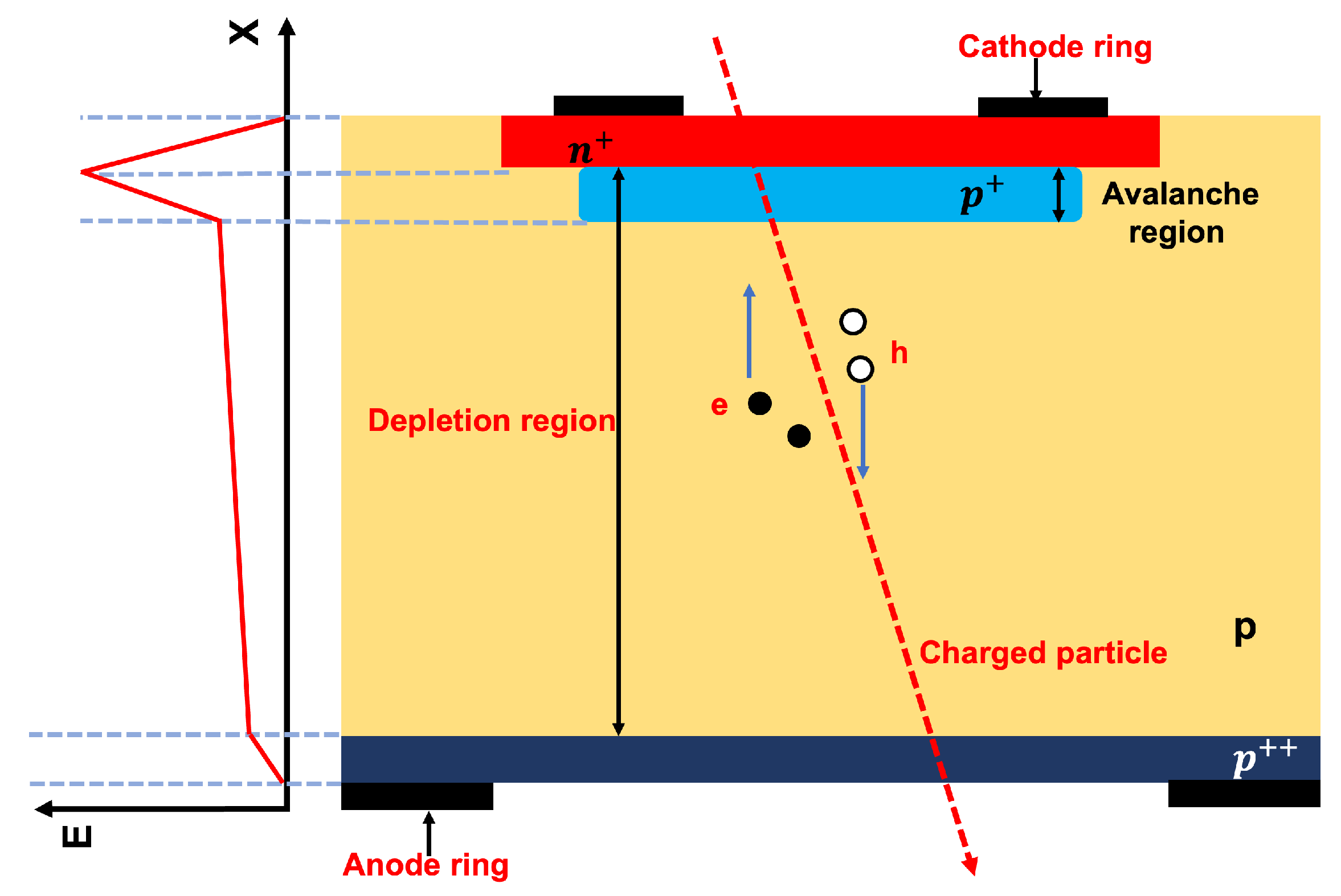
:1. Introduction
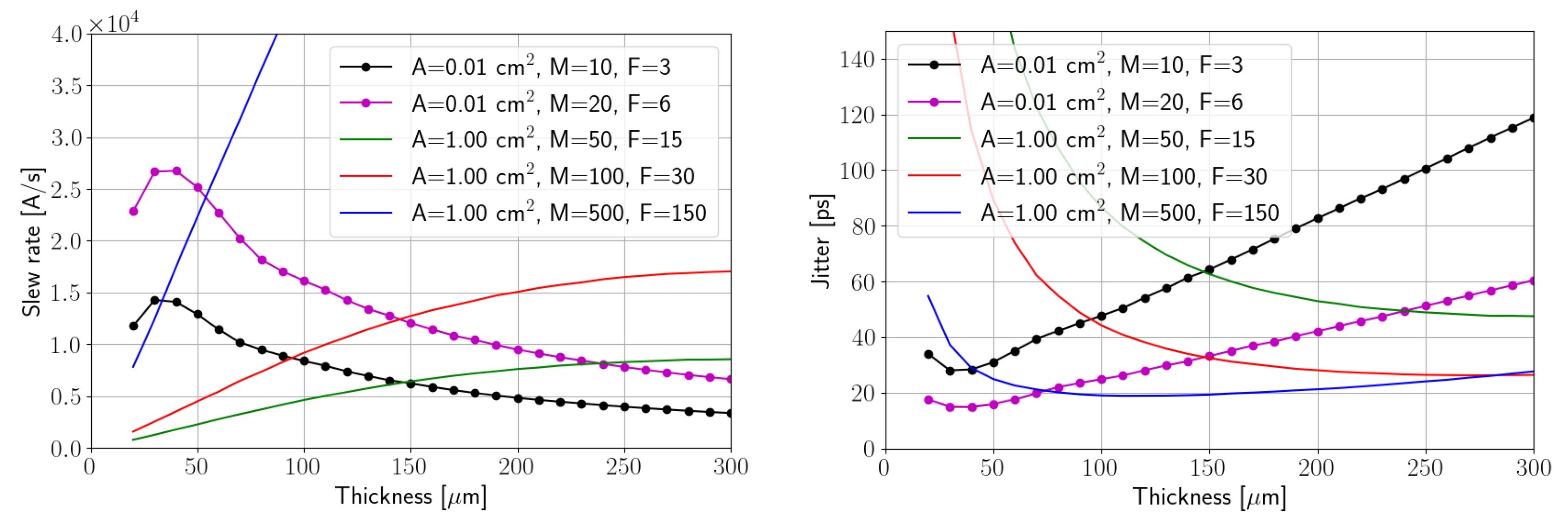
2. Scaling Channel Size: LTspice Simulation
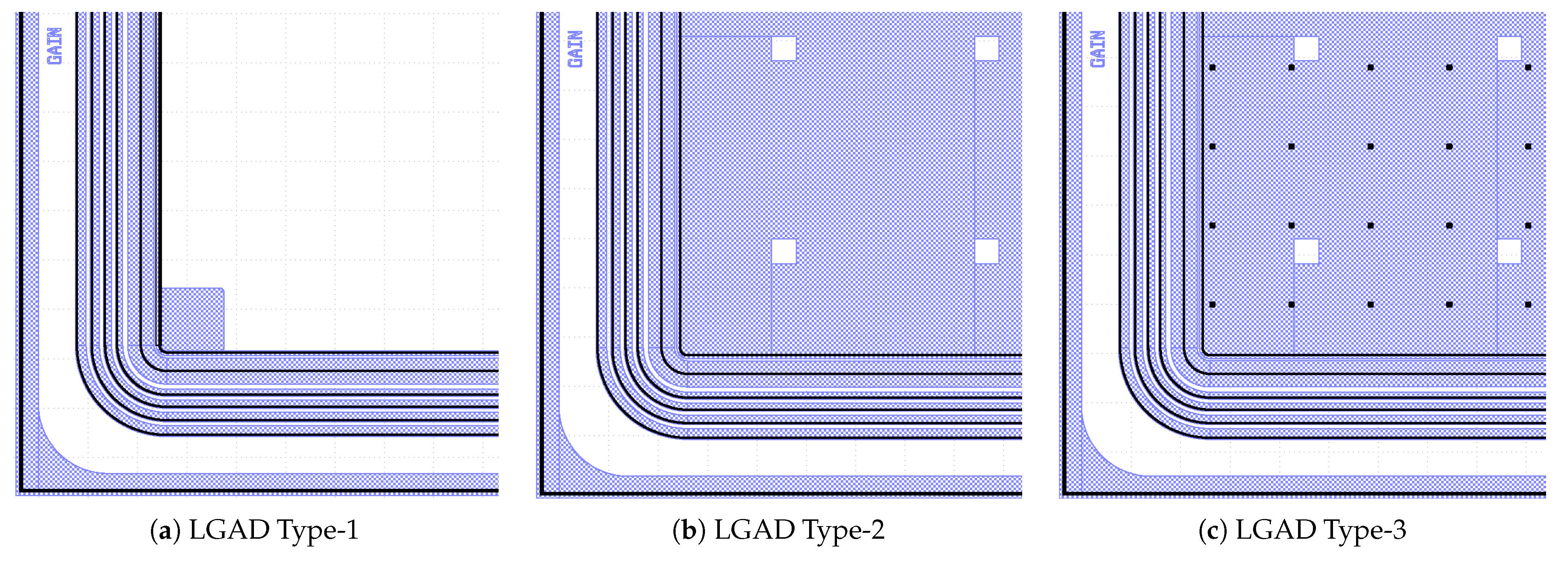
3. LGADs Fabrication
4. Laboratory Measurements
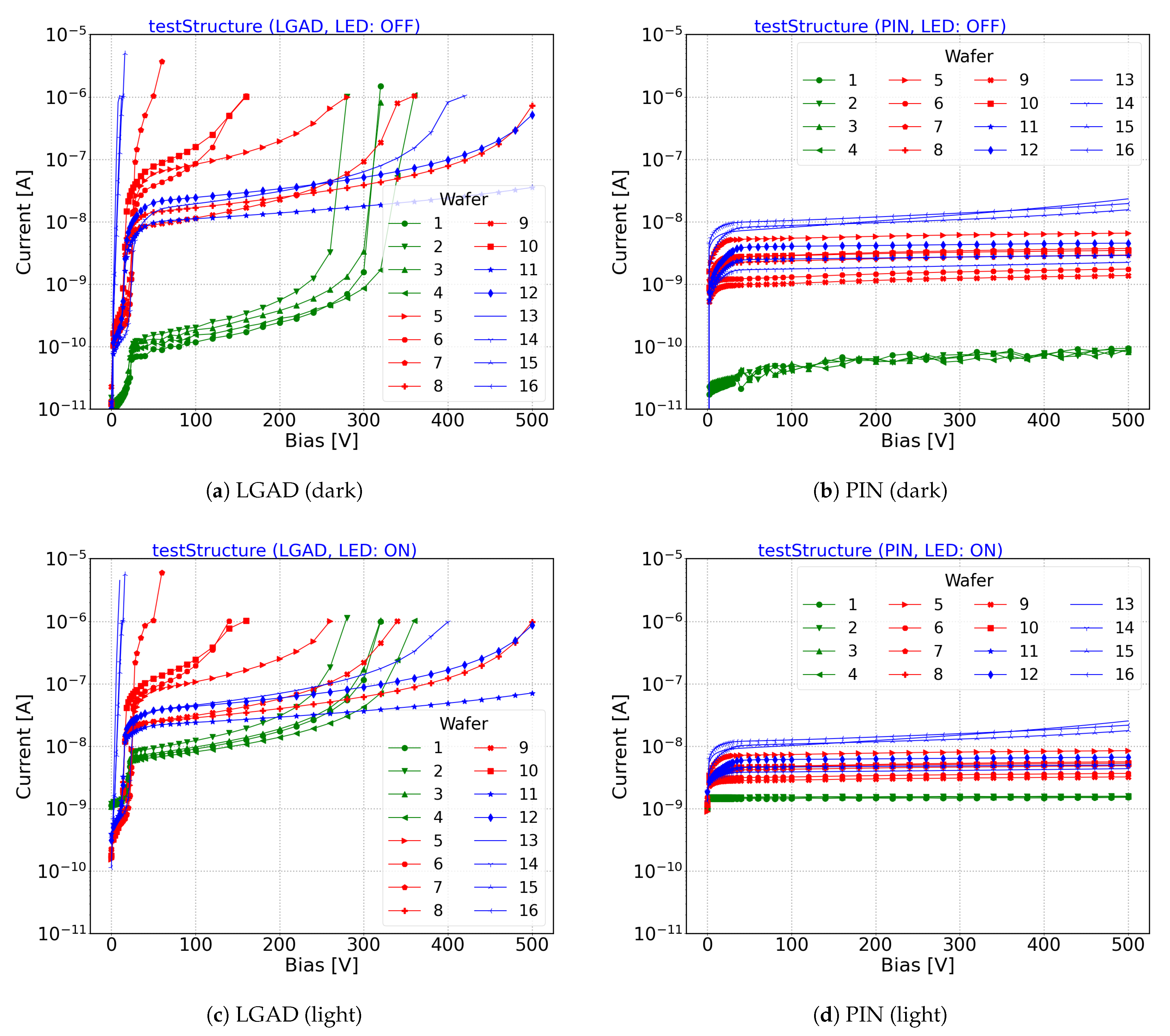
4.1. Leakage Current
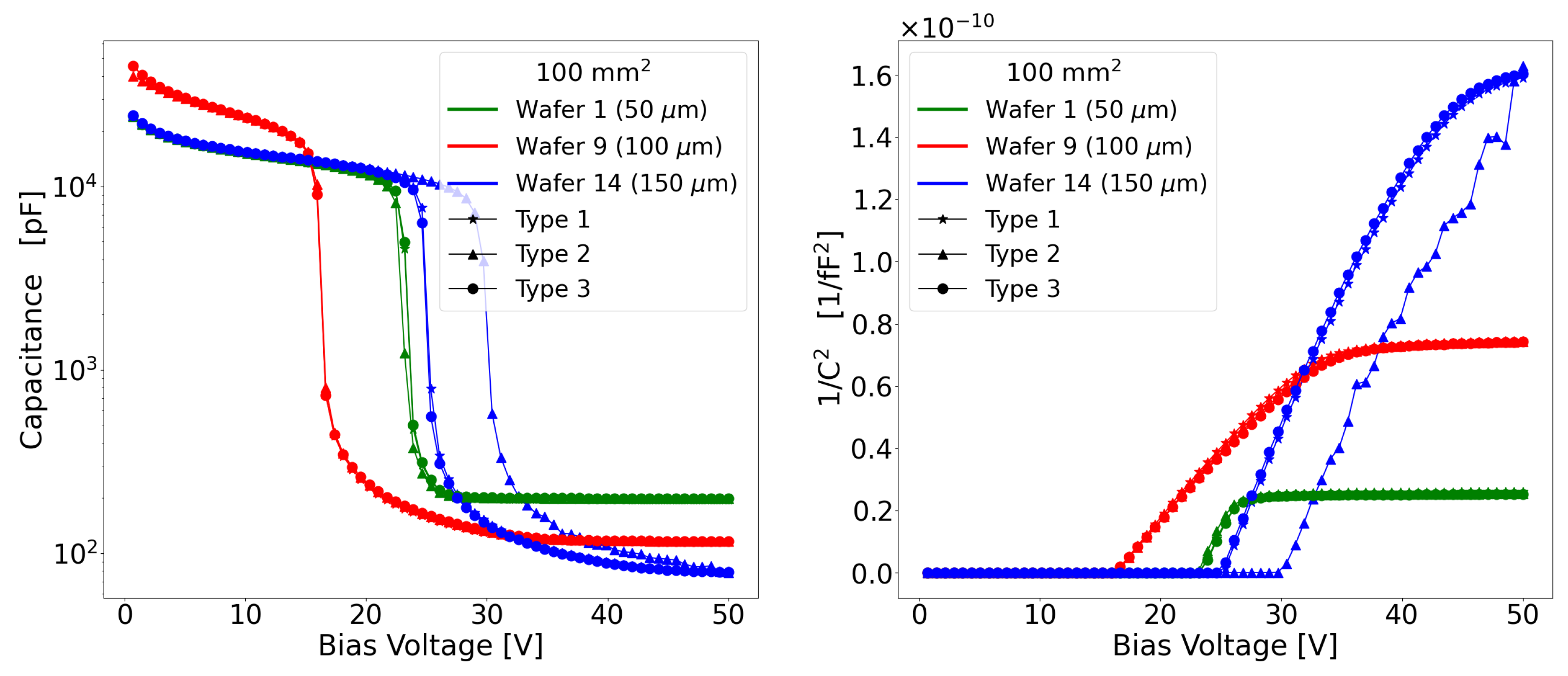
4.2. Capacitance
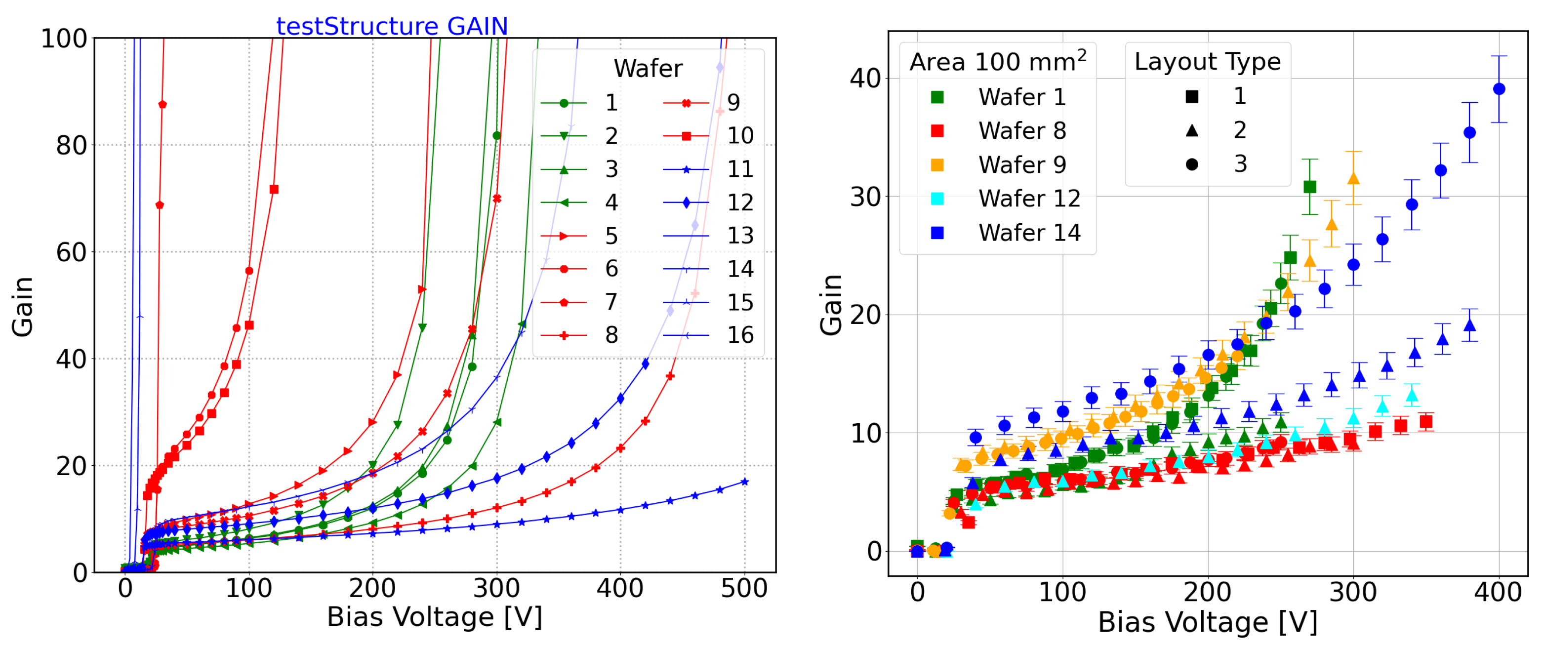
4.3. Gain
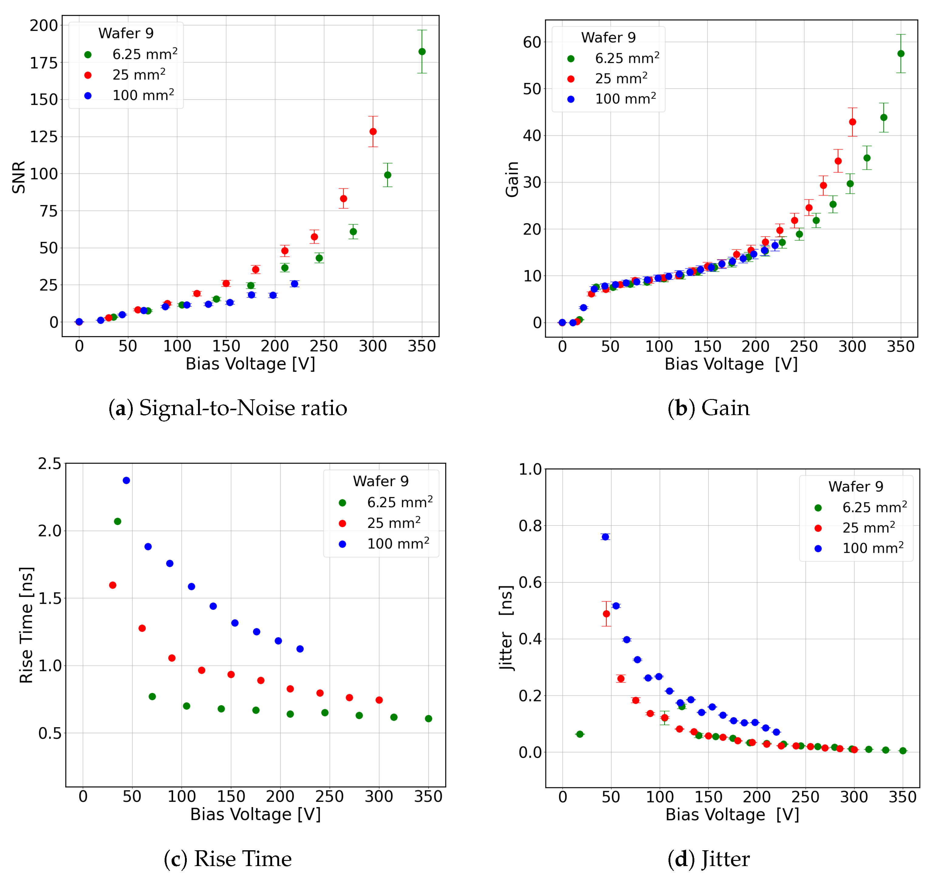
4.4. Time Resolution Study with Laser
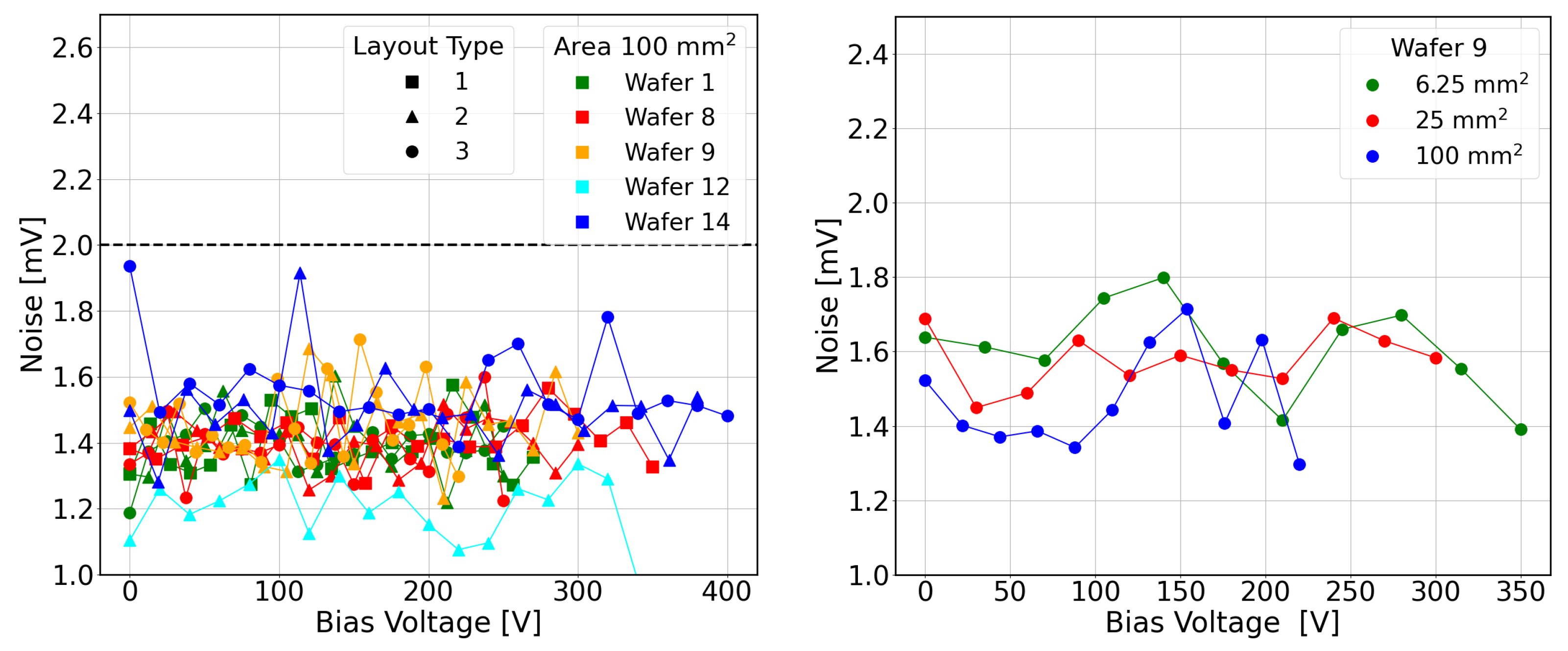
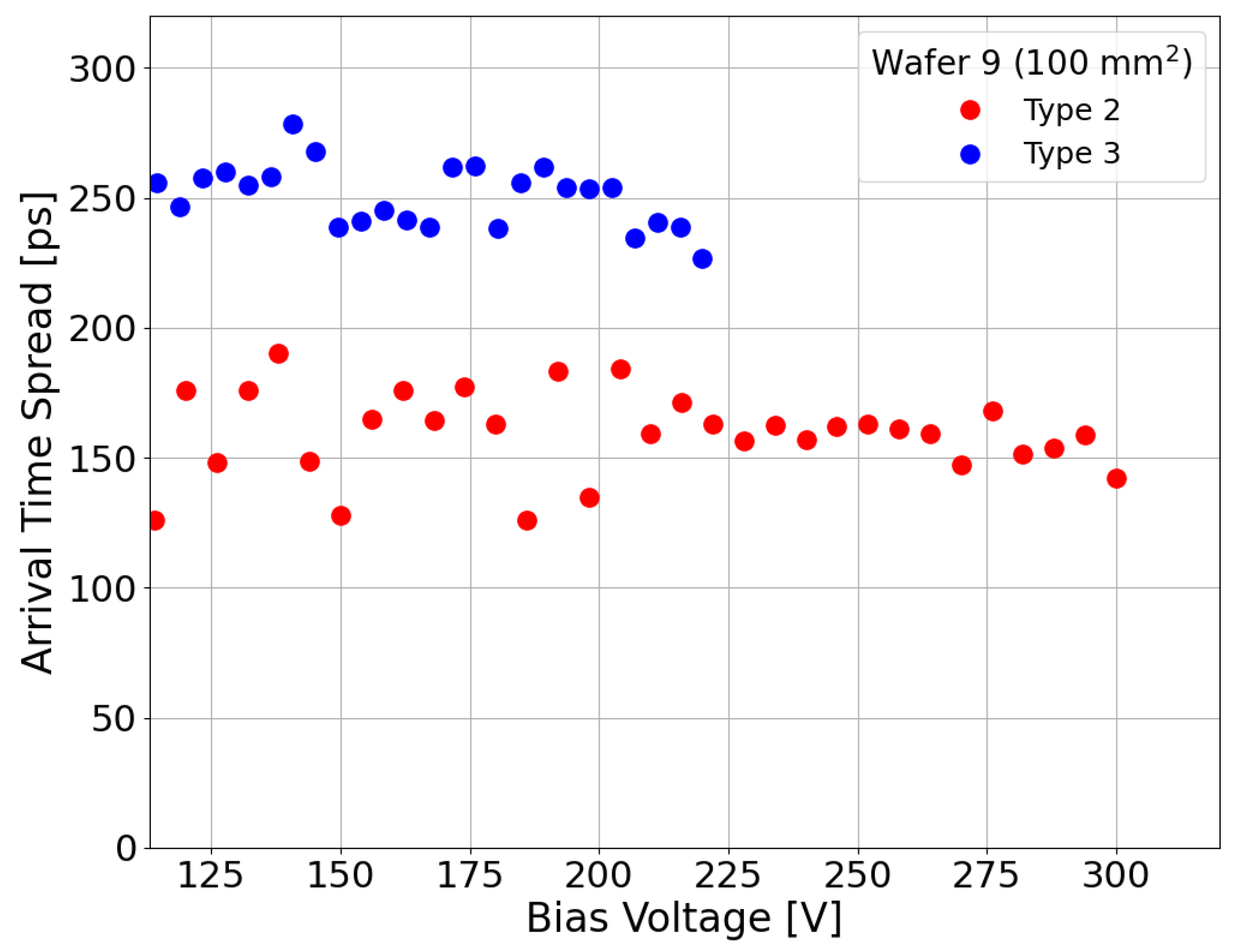
4.5. Uniformity
5. Summary and Conclusions
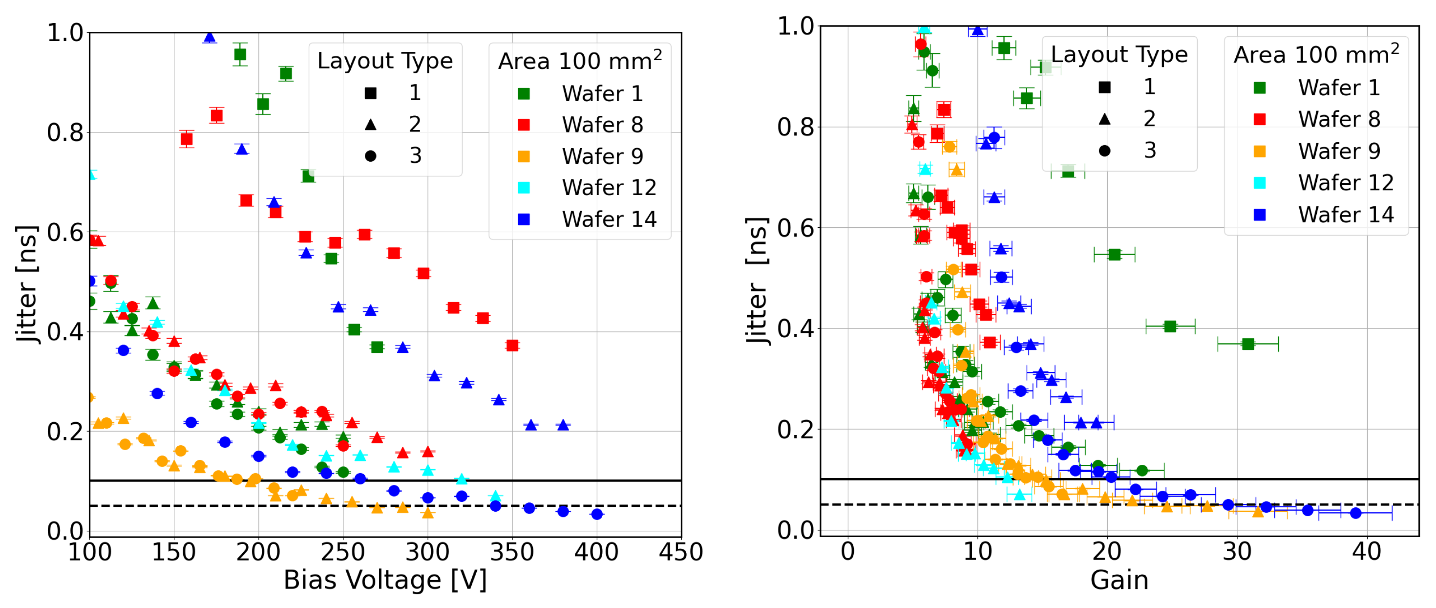
- Electrical measurements (IV) for all the wafers with different gain layer designs indicate that the best gain layer designs to use see a dose of 1.46 and implantation energy of 0.5 for both 100 and 150 µm thicknesses, and a dose of 1.04 with an energy of 1 for 150 µm sensors. The other gain layer designs either go into an early breakdown or have too low a gain.
- A gain value of approximately 40 is achieved at 400 V for wafer 14. However, the LED measurements suggest that a gain of 100 is achievable at a bias voltage greater than 400 V, but the gain curve becomes steeper. If the gain curve is too steep, a small fluctuation in the operating voltage of the sensor will result in a different gain, making the operating condition of the device unstable.
- From the measurements using an IR laser with an intensity set to 1 MIP, a jitter of ∼35 ps can be obtained on LGAD sensors with a 100 mm2 area, with different design configurations.
- The uniformity of response of the sensors was measured using an IR laser. This effect’s contribution to the sensors’ time resolution is estimated to be 44 ps.
Author Contributions
Funding
Institutional Review Board Statement
Informed Consent Statement
Data Availability Statement
Acknowledgments
Conflicts of Interest
Abbreviations
| CCRs | Charged Cosmic Rays |
| CFD | Constant Fraction Discrimination |
| HEP | High-Energy Physics |
| LED | Light Emitting Diode |
| LGADs | Low-Gain Avalanche Diodes |
| MIP | Minimum Ionizing Particle |
| PIN | P-intrinsic-N |
| SLAPP | Space LGADs for Astroparticle Physics |
| SNR | Signal-to-Noise Ratio |
| TCT | Transient Current Technique |
References
- Aguilar, M.; Alcaraz, J.; Allaby, J.; Alpat, B. The Alpha Magnetic Spectrometer (AMS) on the International Space Station: Part I—Results from the test flight on the space shuttle. Phys. Rep. 2002, 366, 331–405. [Google Scholar] [CrossRef]
- Aguilar, M.; Ali Cavasonza, L.; Ambrosi, G.; Arruda, L. The Alpha Magnetic Spectrometer (AMS) on the international space station: Part II—Results from the first seven years. Phys. Rep. 2021, 894, 1–116. [Google Scholar] [CrossRef]
- Tavani, M.; Barbiellini, G.; Argan, A.; Boffelli, F. The AGILE Mission. Astron. Astrophys. 2009, 502, 995–1013. [Google Scholar] [CrossRef]
- Atwood, W.B.; Abdo, A.A.; Ackermann, M.; Althouse, W. The Large Area Telescope on the Fermi Gamma-ray Space Telescope Mission. Astrophys. J. 2009, 697, 1071–1102. [Google Scholar] [CrossRef]
- Picozza, P.; Galper, A.; Castellini, G.; Adriani, O. PAMELA—A payload for antimatter matter exploration and light-nuclei astrophysics. Astropart. Phys. 2007, 27, 296–315. [Google Scholar] [CrossRef]
- Chang, J.; Ambrosi, G.; An, Q.; Asfandiyarov, R. The DArk Matter PARTICLE Explorer mission. Astropart. Phys. 2017, 95, 6–24. [Google Scholar] [CrossRef]
- Alcaraz, J.; Alpat, B.; Ambrosi, G. A silicon microstrip tracker in space: Experience with the AMS silicon tracker on STS-91. Il Nuovo Cimento A (1971–1996) 1999, 112, 1325–1343. [Google Scholar] [CrossRef]
- Duranti, M.; Vagelli, V.; Ambrosi, G.; Barbanera, M.; Bertucci, B.; Catanzani, E.; Donnini, F.; Faldi, F.; Formato, V.; Graziani, M.; et al. Advantages and Requirements in Time Resolving Tracking for Astroparticle Experiments in Space. Instruments 2021, 5, 20. [Google Scholar] [CrossRef]
- Aplin, S.; Boronat, M.; Dannheim, D.; Duarte, J.; Gaede, F.; Ruiz-Jimeno, A.; Sailer, A.; Valentan, M.; Vila, I.; Vos, M. Forward tracking at the next e+e collider part II: Experimental challenges and detector design. J. Instrum. 2013, 8, T06001. [Google Scholar] [CrossRef]
- Pellegrini, G.; Fernández-Martínez, P.; Baselga, M.; Fleta, C.; Flores, D.; Greco, V.; Hidalgo, S.; Mandić, I.; Kramberger, G.; Quirion, D.; et al. Technology developments and first measurements of Low Gain Avalanche Detectors (LGAD) for high energy physics applications. Nucl. Instrum. Meth. 2014, A, 12–16. [Google Scholar] [CrossRef]
- Cartiglia, N.; Staiano, A.; Sola, V.; Arcidiacono, R.; Cirio, R.; Cenna, F.; Ferrero, M.; Monaco, V.; Mulargia, R.; Obertino, M.; et al. Beam test results of a 16ps timing system based on ultra-fast silicon detectors. Nucl. Instrum. Meth. 2017, 850, 83–88. [Google Scholar] [CrossRef]
- Schael, S.; Atanasyan, A.; Berdugo, J.; Bretz, T. AMS-100: The next generation magnetic spectrometer in space—An international science platform for physics and astrophysics at Lagrange point 2. Nucl. Instrum. Methods Phys. Res. Sect. A Accel. Spectrom. Detect. Assoc. Equip. 2019, 944, 162561. [Google Scholar] [CrossRef] [PubMed]
- Kramberger, G.; Carulla, M.; Cavallaro, E.; Cindro, V.; Flores, D.; Galloway, Z.; Grinstein, S.; Hidalgo, S.; Fadeyev, V.; Lange, J.; et al. Radiation hardness of thin Low Gain Avalanche Detectors. Nucl. Instrum. Methods Phys. Res. Sect. A Accel. Spectrom. Detect. Assoc. Equip. 2018, 891, 68–77. [Google Scholar] [CrossRef]
- Analog Devices LTspice Official Website. Available online: https://www.linear.com/LTspice (accessed on 14 March 2022).
- Bichsel, H. Straggling in thin silicon detectors. Rev. Mod. Phys. 1988, 60, 663–699. [Google Scholar] [CrossRef]
- Dalla Betta, G.F.; Pancheri, L.; Boscardin, M.; Paternoster, G.; Piemonte, C.; Cartiglia, N.; Cenna, F.; Bruzzi, M. Design and TCAD simulation of double-sided pixelated low gain avalanche detectors. Nucl. Instrum. Methods Phys. Res. Sect. A Accel. Spectrom. Detect. Assoc. Equip. 2015, 796, 154–157. [Google Scholar] [CrossRef]
- Cividec Instrumentation. Available online: https://cividec.at/index.php?module=public.product&idProduct=34&scr=0 (accessed on 21 September 2022).
- Teich, M.; Matsuo, K.; Saleh, B. Excess noise factors for conventional and superlattice avalanche photodiodes and photomultiplier tubes. IEEE J. Quantum Electron. 1986, 22, 1184–1193. [Google Scholar] [CrossRef]
- Scharf, C.; Klanner, R. Measurement of the drift velocities of electrons and holes in high-ohmic <100> silicon. Nucl. Instrum. Methods Phys. Res. Sect. A Accel. Spectrom. Detect. Assoc. Equip. 2015, 799, 81–89. [Google Scholar] [CrossRef]
- SILVACO TCAD: Semiconductor Process and Device Simulation. Available online: https://silvaco.com/tcad/ (accessed on 4 November 2022).
- Bisht, A. Development of Low Gain Avalanche Detectors for Astroparticle Physics Experiments in Space. Ph.D. Thesis, Univeristà degli Studi di Trento, Trento, Italy, 2023. [Google Scholar]
- Heller, R.; Abreu, A.; Apresyan, A.; Arcidiacono, R.; Cartiglia, N.; DiPetrillo, K.; Ferrero, M.; Hussain, M.; Lazarovitz, M.; Lee, H.; et al. Combined analysis of HPK 3.1 LGADs using a proton beam, beta source, and probe station towards establishing high volume quality control. NIMA 2021, 1018, 165828. [Google Scholar] [CrossRef]
- Large Scanning TCT Setup, Particulars. Available online: http://particulars.si/index.php (accessed on 7 June 2023).
- Currás Rivera, E.; Moll, M. Study of Impact Ionization Coefficients in Silicon with Low Gain Avalanche Diodes. IEEE Trans. Electron Devices 2023, 70, 2919–2926. [Google Scholar] [CrossRef]
- Siviero, F.; Arcidiacono, R.; Borghi, G.; Boscardin, M.; Cartiglia, N.; Vignali, M.C.; Costa, M.; Dalla Betta, G.-F.; Ferrero, M.; Ficorella, F.; et al. Optimization of the gain layer design of ultra-fast silicon detectors. Nucl. Instrum. Methods Phys. Res. Sect. A Accel. Spectrom. Detect. Assoc. Equip. 2022, 1033, 166739. [Google Scholar] [CrossRef]


| Area (cm2) | Gain (M) | Excess Noise Factor (F) |
|---|---|---|
| 0.01 | 10 | 3 |
| 20 | 6 | |
| 1 | 10 | 3 |
| 100 | 30 | |
| 500 | 150 |
| Thickness (µm) | Wafer | Dose | Gain Dose | Gain Energy |
|---|---|---|---|---|
| 50 | 1 | 1 | 0.98 | 1 |
| 2 | 1 | 1 | 1 | |
| 3 | 3 | 1 | 1 | |
| 4 | 3 | 0.98 | 1 | |
| 100 | 5 | 1 | 1.04 | 1 |
| 6 | 1 | 1.08 | 1 | |
| 7 | 1 | 1.12 | 1 | |
| 8 | 1 | 1.4 | 0.5 | |
| 9 | 1 | 1.46 | 0.5 | |
| 10 | 1 | 1.52 | 0.5 | |
| 150 | 11 | 1 | 1.4 | 0.5 |
| 12 | 1 | 1.46 | 0.5 | |
| 13 | 1 | 1.52 | 0.5 | |
| 14 | 1 | 1.04 | 1 | |
| 15 | 1 | 1.08 | 1 | |
| 16 | 1 | 1.12 | 1 |
Disclaimer/Publisher’s Note: The statements, opinions and data contained in all publications are solely those of the individual author(s) and contributor(s) and not of MDPI and/or the editor(s). MDPI and/or the editor(s) disclaim responsibility for any injury to people or property resulting from any ideas, methods, instructions or products referred to in the content. |
© 2024 by the authors. Licensee MDPI, Basel, Switzerland. This article is an open access article distributed under the terms and conditions of the Creative Commons Attribution (CC BY) license (https://creativecommons.org/licenses/by/4.0/).
Share and Cite
Bisht, A.; Cavazzini, L.; Centis Vignali, M.; Caso, F.; Hammad Ali, O.; Ficorella, F.; Boscardin, M.; Paternoster, G. Jitter Measurements of 1 cm2 LGADs for Space Experiments. Instruments 2024, 8, 27. https://doi.org/10.3390/instruments8020027
Bisht A, Cavazzini L, Centis Vignali M, Caso F, Hammad Ali O, Ficorella F, Boscardin M, Paternoster G. Jitter Measurements of 1 cm2 LGADs for Space Experiments. Instruments. 2024; 8(2):27. https://doi.org/10.3390/instruments8020027
Chicago/Turabian StyleBisht, Ashish, Leo Cavazzini, Matteo Centis Vignali, Fabiola Caso, Omar Hammad Ali, Francesco Ficorella, Maurizio Boscardin, and Giovanni Paternoster. 2024. "Jitter Measurements of 1 cm2 LGADs for Space Experiments" Instruments 8, no. 2: 27. https://doi.org/10.3390/instruments8020027