Article

Development of High-Voltage Electrodes for Neutron Scattering Sample Environment Devices

1
Faculty of Mechanical and Electrical Engineering, Kunming University of Science and Technology, Kunming 650500, China
2
Institute of High Energy Physics, Chinese Academy of Sciences, Beijing 100049, China
3
Spallation Neutron Source Science Centre, Dongguan 523803, China
*
Authors to whom correspondence should be addressed.
Instruments 2024, 8(2), 26; https://doi.org/10.3390/instruments8020026
Submission received: 12 February 2024 / Revised: 25 March 2024 / Accepted: 27 March 2024 / Published: 28 March 2024

Abstract

:
The sample environment is essential to neutron scattering experiments as it induces the sample under study into a phase or state of particular interest. Various sample environments have been developed, yet the high-voltage electric field has rarely been documented. In this study, Bruce electrodes with various sectional geometries and chamber sizes were examined by using simulation modeling based on ANSYS Maxwell. A large uniform field region where samples would sit could be achieved in the planar region for all specifications, but the size of the region and the field strength varied with the gap distance between electrodes. The edging effect was inherently observed even for bare electrodes, about 1.7% higher in the sinusoidal region than the planar region, and was significantly deteriorated when a chamber was applied. This effect, however, presented an exponential decrease as the minimum distance between the electrode edge and the chamber shell increased. A compromise between the spatial confinement and the achievable field (strength and uniform region) could be reached according to the unique applicability of neutron instruments. This research provides a theoretical basis for the subsequent design and manufacturing of high-voltage sample environment devices.

1. Introduction

The neutron scattering technique has been playing an important role in understanding the changes in nanostructure and dynamics of materials at the atom level correlated to their physicochemical properties. It is particularly powerful in the study of advanced materials under various extreme conditions owing to the high penetration of neutrons, such as low temperature, gas treatment, high pressure, high temperature, and strong magnetic field [1,2,3]. It has been demonstrated that more than 95% of neutron scattering experiments were performed with some kind of sample environments [4]. The development of sample environments in various neutron sources around the world has been reported in review articles [5], the information about the systematical development and application of high-voltage electric field devices for neutron scattering experiments, however, has rarely been mentioned [6]. This is mainly because of the contact issue and breakdown concerns, especially when the electrodes have to be confined within a tiny sample space and/or coupled with other conditions normally required for neutron scattering measurements.
The electric field has been identified as one of the most important external forces for modulating the physicochemical properties of materials [7,8], controlling the structure, anisotropy, and performance of composite materials [9], preparing superconducting materials [10,11,12], exploring the magnetic and electrical properties of materials for various electronic devices [13,14], and developing new hydrogen storage materials [15] and biomedicines [16,17]. It has therefore attracted the interest of scientists in studying the changes in nanostructure and atomic dynamics under a high-voltage electric field by in situ using neutron scattering techniques.
An electric field device using needle-shaped electrodes developed by Lucy K. Saunders et al. [18] required complicated experimental operations and sample installations. The local Joule heat and even breakdown occurred when a high voltage was applied due to the inhomogeneous field strength. The identical problems were also observed in a special electric field device developed by T. Yu. Vergenteva et al. [19] for single-crystal diffraction experiments. A DC electric field from two parallel plates was applied for examining phase transitions in soft matter systems but the field uniformity was not considered at all [20]. Very recently, a temperature-controlled electric field device was developed for small-angle neutron scattering experiments [21]. The device may work well for some materials/measurements but will be significantly limited when a much higher field strength is required due to the thin layer and edging effect.
Field uniformity and strength are crucial to the development of high-voltage electric field devices, particularly for large-scale neutron instruments such as the small-angle neutron scattering (SANS) instrument and neutron reflectometer (NR), which mainly focus on the study of the composition and nanostructure (size and anisotropy) of materials, ranging from one to several hundred nanometers by using either a transmission or a reflection mode. In those cases, the overall goal of an electric field device is to generate an as high and uniform electric field as possible while minimizing local field enhancement effects on any other part of the electrode assembly relative to the central ideal electric field region [22]. The uniformity is critical not only along the gap axis between the electrodes but also along the surface of each electrode plate within a specified area. Theoretically, an ideal uniform field can be produced by two electrodes with parallel planes of infinite size. However, the space required for ongoing SANS/NR experiments is strictly limited, and as a consequence, the size of the device (including electrodes and shielding chamber) will crucially affect field uniformity, thereby limiting its practicability. The edging effect, on the other hand, will significantly limit the achievable field strength and therefore should be strictly avoided or minimized. Previous researchers have developed various electrode profiles to avoid the edging effect, ranging from simple planar to more complex elliptical [23], Rogowski [24], and Bruce [25] profiles, but the applicability of those profiles, particularly the compromise between field uniformity and strength and the spatial confinement for neutron scattering experiments, has not yet been examined.
The finite element method (FEM) has been extensively used in electric field analysis due to its flexibility and simplicity, allowing the estimation of fields on thin and highly curved electrode surfaces using various dielectric materials [26,27,28,29,30]. It calculates the field strength and potential distribution in a high-voltage electric field by discretizing the electrode domain and thereby even solving problems with complex geometries [31]. In this research, a two-dimensional FEM model was developed from the real geometric dimension for the calculation of the field strength and potential distribution of high-voltage electrodes with various geometries and chamber sizes by using ANSYS Maxwell software. The electrode specifications and the corresponding sample chamber size were defined for the further development of the high-voltage sample environment for neutron scattering experiments, providing theoretical guidance for the subsequent manufacture and assembly of high-voltage electric field devices.

2. Electric Field Modeling

The equation satisfied by the curl of the electric field intensity and the scattering of the electric displacement vector is the differential form of the fundamental equation of the electrostatic field [32]:
· D = ρ
where D is the electric displacement vector and ρ is the bulk density of free charges. In an isotropic dielectric, the auxiliary equation is:
D = ε · E
where ε is the permittivity of the dielectric, also known as permittivity, and E is the electric field. Substituting Equation (2) into (1), one can obtain:
D = · ( ε E ) = ε · E + E · ε = ρ
In a homogeneous dielectric, ε = 0. In addition, the electric field strength E = φ can be substituted into Equation (3) to obtain:
ε 2 φ = ρ
where φ is the electric potential. It can be therefore concluded that Equation (4) is the Poisson equation of the electrostatic field. When there is no charge distribution in the field, ρ = 0, then Equation (4) becomes:
ε 2 φ = 0
In a high-voltage device, the space charge does not exist or is negligible (ρ = 0), so the dielectric equation to be solved is actually Equation (5), where 2 is the Laplace operator and in the Cartesian coordinate system it is:
2 φ = 2 φ x 2 + 2 φ y 2 + 2 φ z 2
The computer can solve the partial differential equation of Formula (6) and obtain the potential distribution of the conductor in a space or a plane area by using FEM via setting the boundary conditions. Various physical properties of the electrostatic field can also be obtained after post-processing the finite element software. As a consequence, the distribution of potential and field intensity in the solution area can be calculated by using the known free charge distribution if the potential on the boundary is given. This type of problem is usually called the first type of boundary value problem, also known as the Diliheri problem [32], which can be expressed as:
ε 2 φ = 0
φ | Γ = φ 0

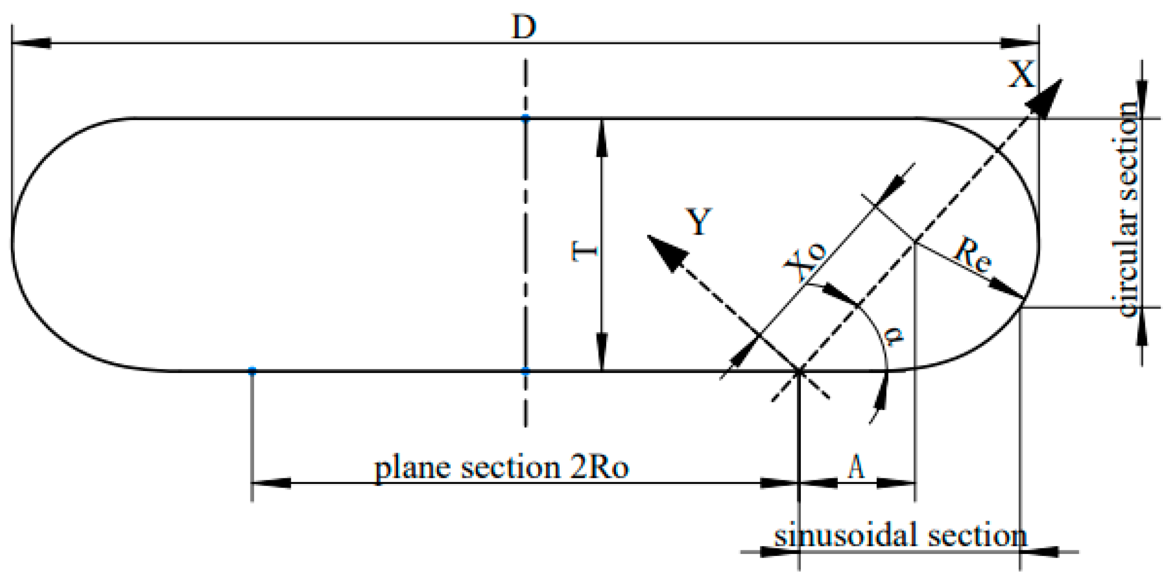
3. Electrode Profile

Based on the previously developed electrode profiles [33], the Bruce electrode composed of three sections produces a uniform field within a large plane area compared to the planar and elliptical profiles and requires relatively smaller space than the Rogowski (90° and 120°) profiles. The first part starts from the linear section with a radius of R0 (Figure 1). The second part is sinusoidal with a radial extension distance of A (distance from the endpoint of the plane area to the center of the circular part), terminated in a circular part with a radius of Re. Each section needs to tangentially merge into the next. The smoothness and specifications of each section, however, need to be further confirmed and improved through simulations. It has to be mentioned that field uniformity also significantly relies on the ratio between the overall diameter (D) and gap distance of electrodes (d) [22].
To guarantee a smooth transition between the numerous components from the Bruce profile, Re and X0 must be defined as follows [33]:
X 0 = A cos α
R e = 2 π · X 0 · tan α
where α is the characteristic angle of the sinusoidal curve. The total radius R and electrode thickness T of the Bruce electrode can be expressed as:
R = R 0 + A + R e = R 0 + A + 2 π A cos α tan α
T = A · tan α + R e = A · tan α ( 1 + 2 π 1 cos α )
To ensure the sample region where subjects a uniform electric field is big enough, yet still acceptable by the spatial confinement, the radius of plane area (R0) was selected as 40 mm for the subsequent simulations. Previous studies on the surface field distribution of electrodes confirmed that a uniform field intensity distribution could be obtained when the electrode thickness was maintained equal to or more than twice the nominal gap spacing [33]. Therefore, the gap spacing (d) in the simulations is always half of the electrode thickness (T) for saving space. From Equations (11) and (12), one can see that R and T are both highly related to A and α. The smaller the characteristic angle in the sinusoidal region, the smaller the T and R, leading to a smaller interval. Otherwise, a much bigger gap distance between the electrodes will be required when the characteristics angle of the sinusoidal section is increased. The space for integrating other modules or coupling with other conditions will be significantly limited in that case. Five potential electrodes with various geometries were examined with respect to the uniformity and strength of the electric field (Table 1).

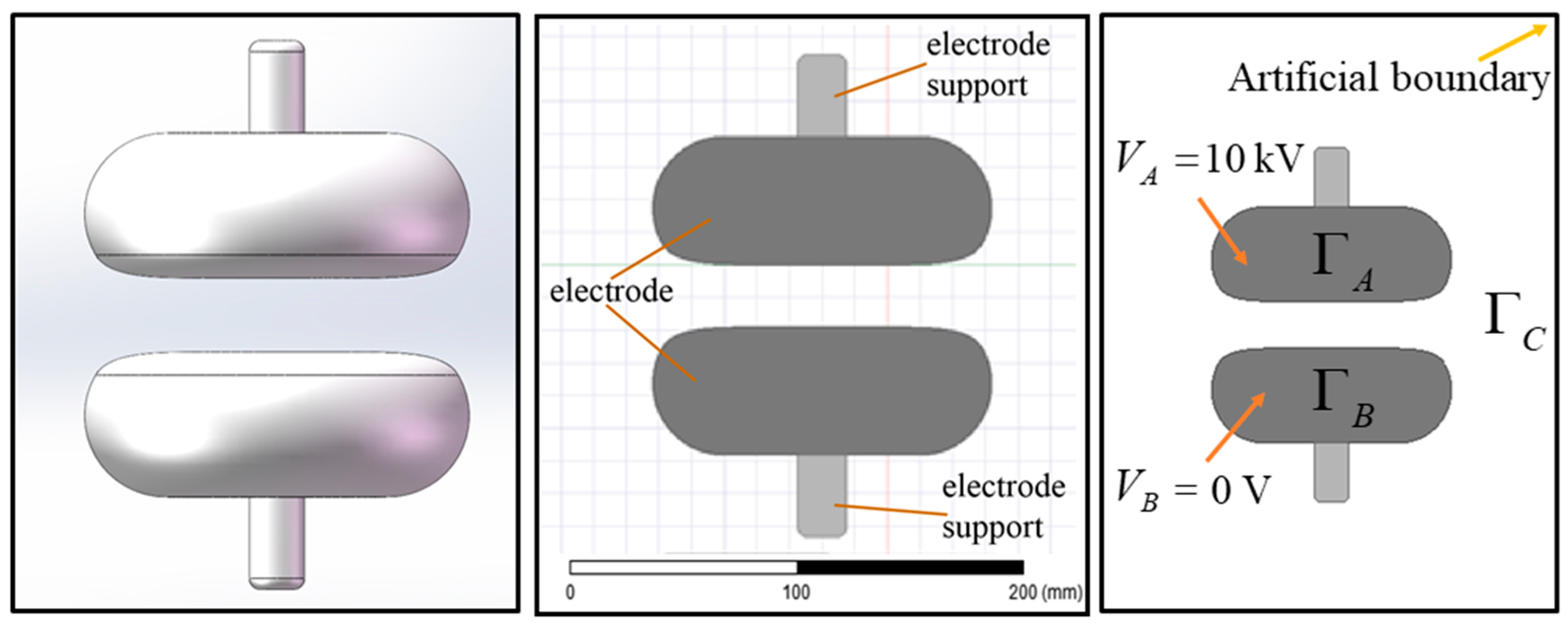
4. Electric Field Simulation

ANSYS Maxwell is a high-end interactive tool for electromagnetic simulation using FEM. After obtaining definitive results, Maxwell solves the electromagnetic field problems by applying Maxwell’s equations in a finite region with suitable boundary settings as well as user-specified parameters [27]. All simulations in this study were performed using Maxwell 2D, with the solver classified as an electrical solution type. Precise modeling was performed initially by using SolidWorks to create a 3D model (Figure 2, left) of the simulated electrode according to the functional relationship of the electrode profile, which was then imported into ANSYS Maxwell software to create a 2D electrode model around the z-axis (Figure 2, middle).
The computational domain for the simulation was set to be a 592 × 416 mm box (Figure 2, right). The boundary conditions used for the simulation were as follows: anode φ | Γ A = 10 kV (targeted value); cathode ground φ | Γ B = 0 V; and the voltage at infinity was an artificial boundary. The high-voltage electrode composed of a Bruce electrode and electrode support possessed a symmetrical geometry. The anode and cathode were built up from aluminum with a relative permittivity ( ε r ) of 1 and a bulk conductivity of 38 × 106 Siemens/m due to a much higher breakdown voltage. Polyether ether ketone (PEEK) with an ε r of 3.1 and a bulk conductivity of 10 × 107 Siemens/m was applied as the electrode support because of its high temperature resistance and good insulation performance. All parameters of the applied materials in the simulation are listed in Table 2.

5. Results and Discussion

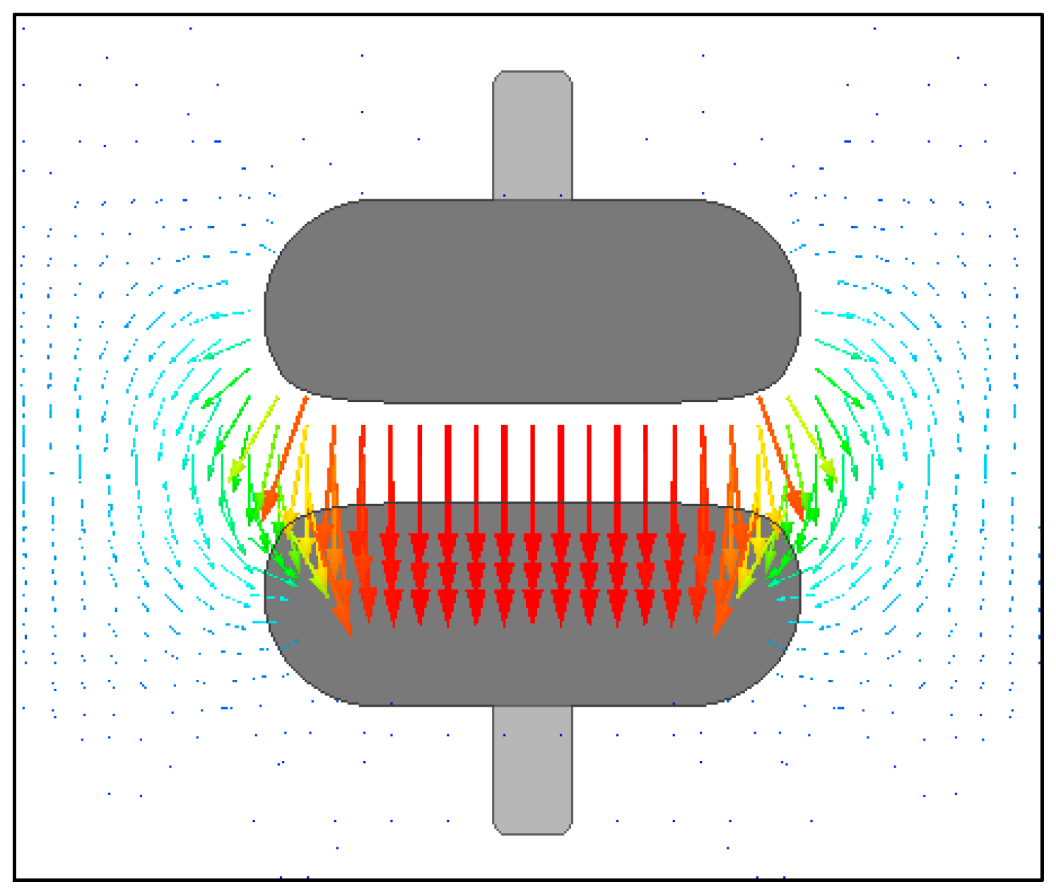
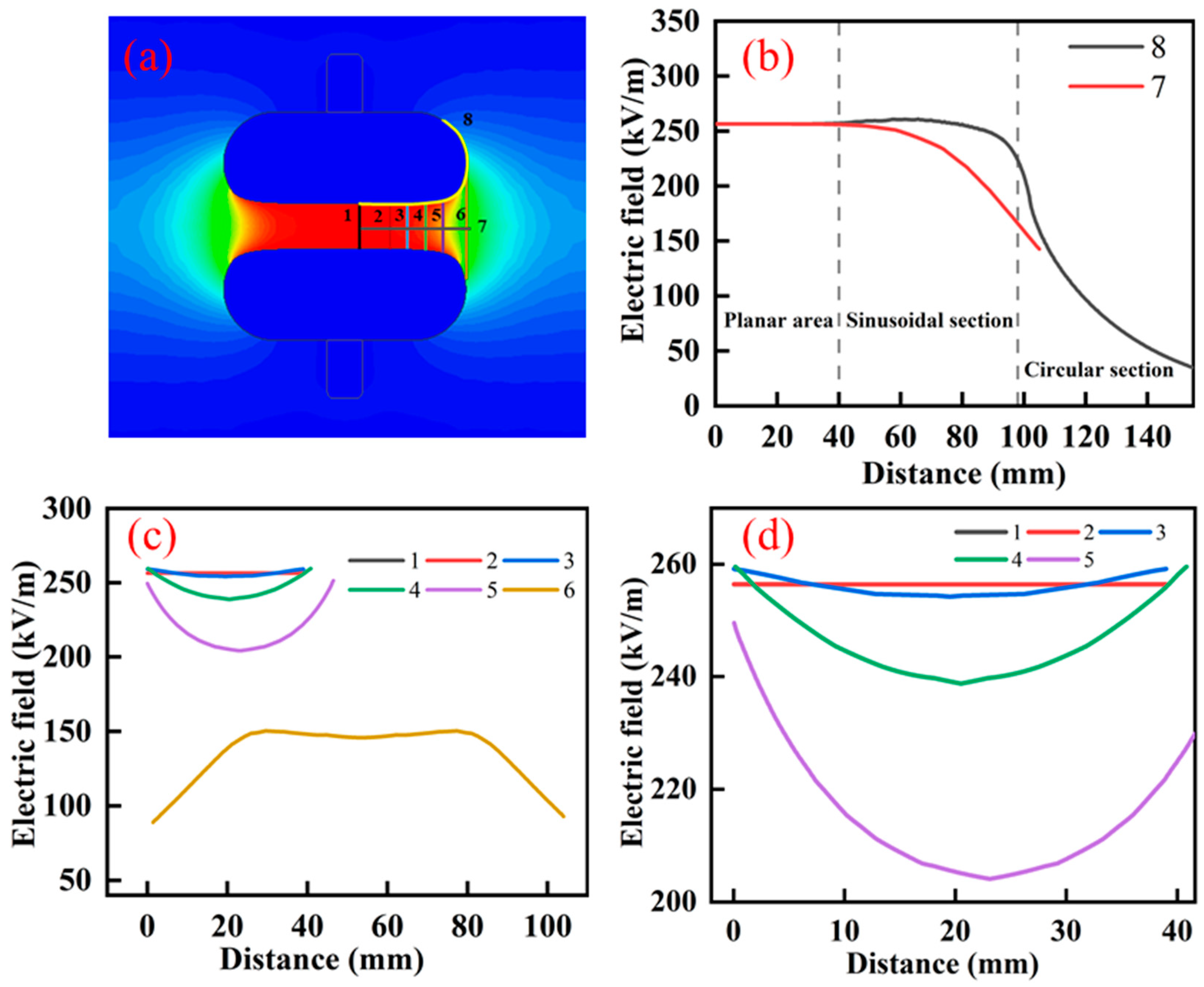
5.1. Electric Field Distribution

The electric field vectors can be clearly outlined to give an insight into the motion of the electric field and then describe the estimated magnitude and strength when a voltage is applied. It can be seen that at any point (Figure 3), the field vector determines the field direction from that point. The movement of the electric field is always from anode to cathode and the field strength varies point by point with the strongest points found between the electrodes in red.

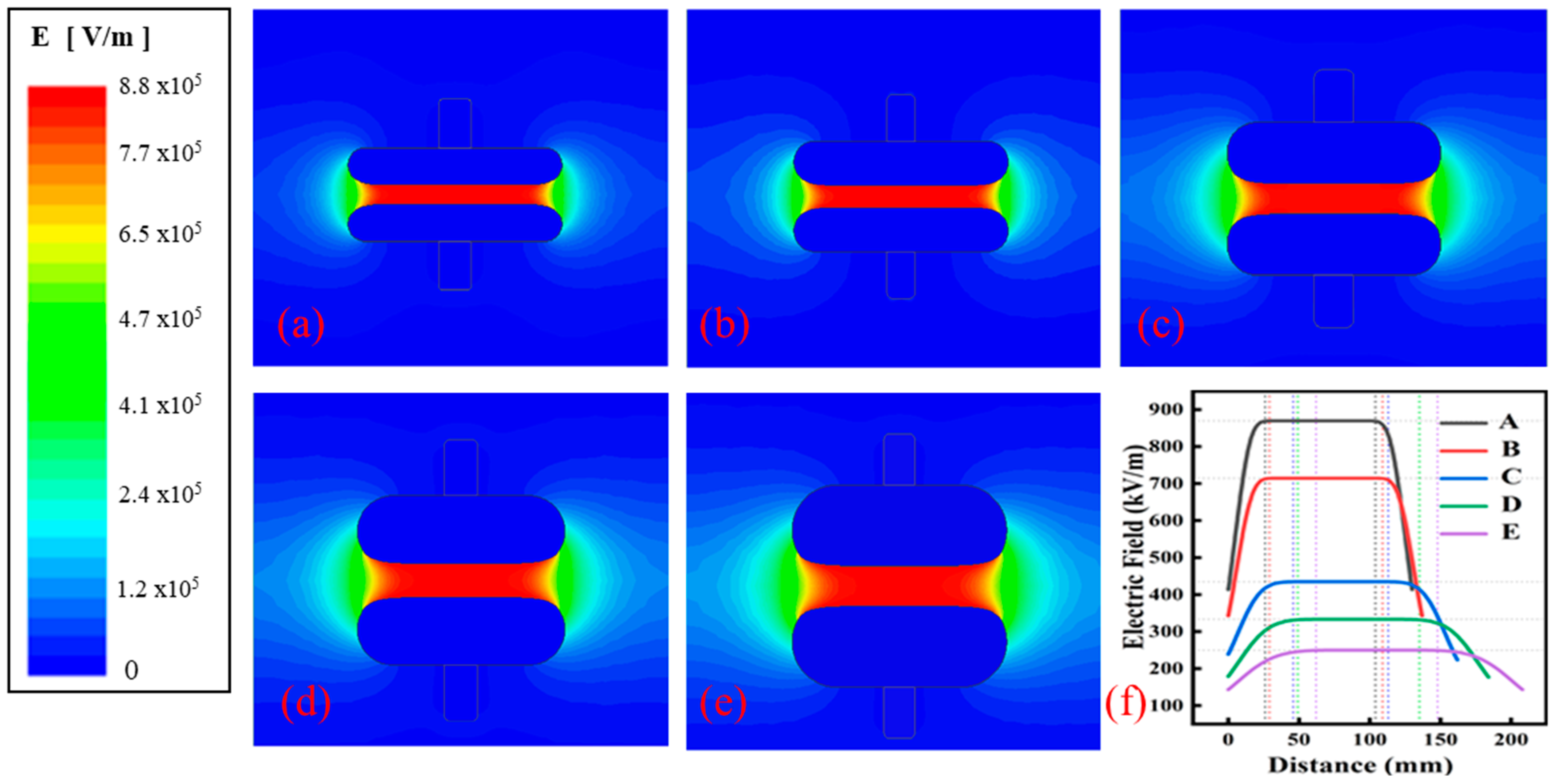
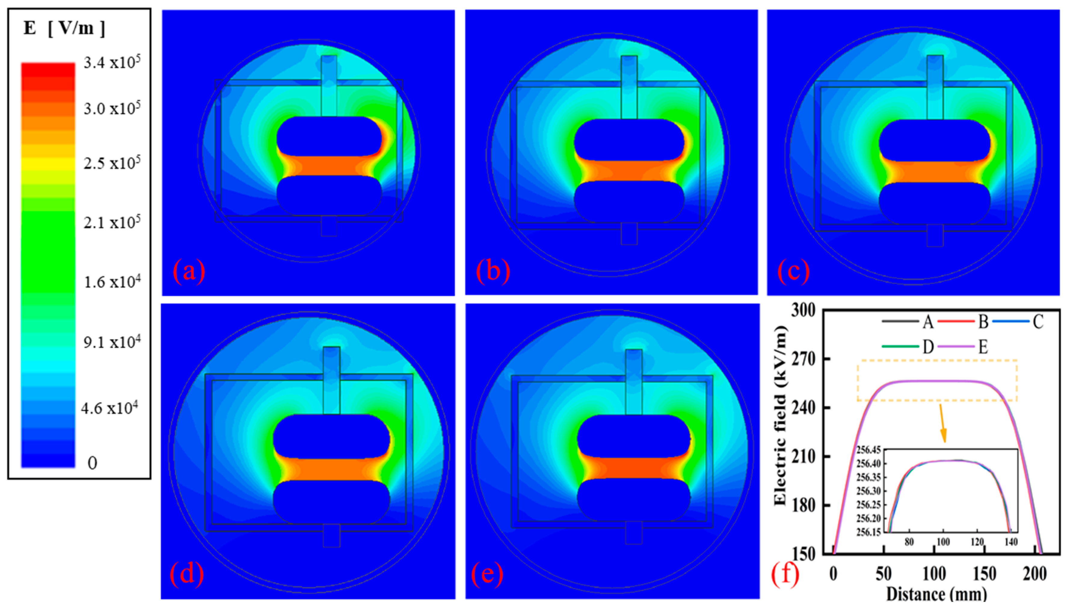
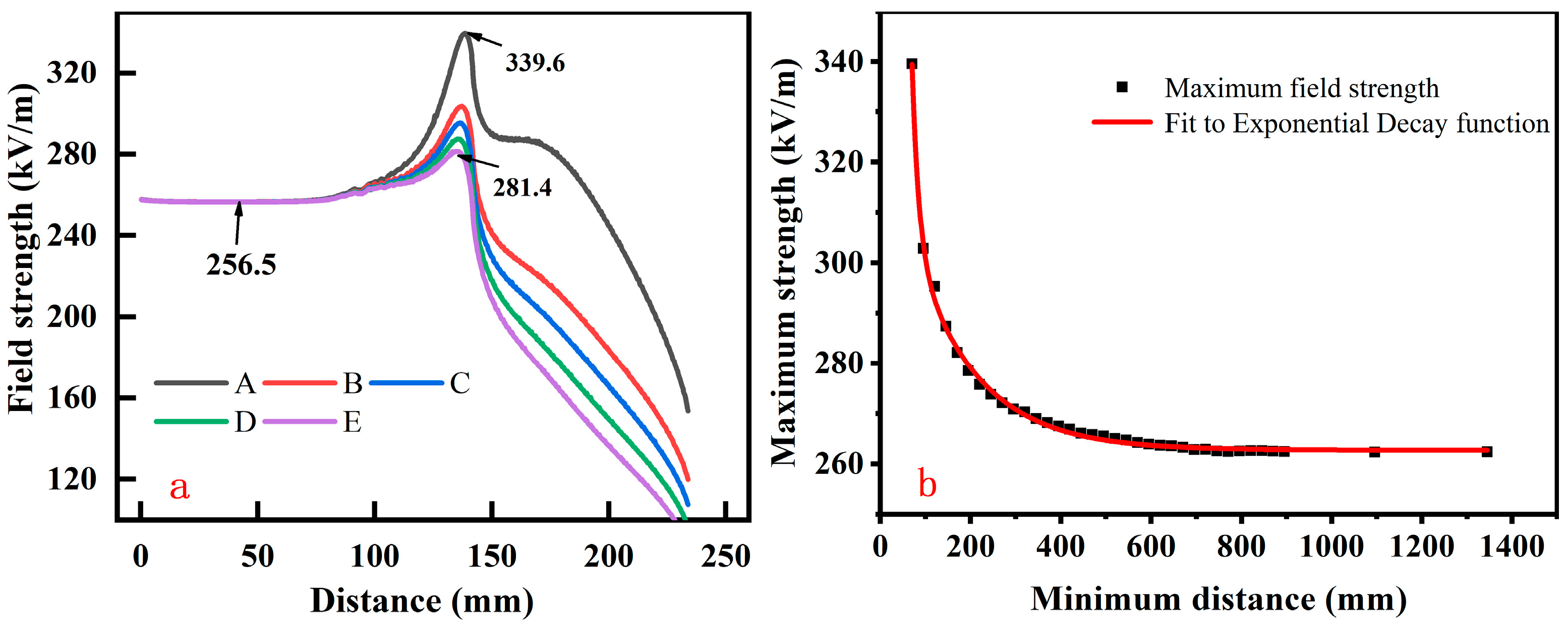
5.2. Effect of Electrode Geometries on Field Intensity and Uniformity

By setting the same voltage excitation value (10 kV), boundary conditions and network division for electrostatic simulations, the field strength distribution varies with the geometry of an electrode imported into ANSYS Maxwell (Figure 4). The highest electric field is undoubtedly found between the electrodes in red, though the strength is highly dependent on the gap spacing. By plotting the field strength along a line shown in Model E for all models (Figure 4f), it can be seen that the maximum field strength generated is 8.84 × 10⁵ V/m (Model A), and as the electrode gap distance increases, the field strength gradually decreases to 2.89 × 10⁵ V/m (Model E). A homogenous field along the line can be achieved within a specified region in each model, but the region size and the achievable strength vary with the geometry.
The uniformity of the field strength along and normal to the electrode gap axis of Model E in various sections/positions was examined to further confirm the region where the sample would sit (Figure 5a). Line 1 is exactly located in the middle of the electrode, lines 2 and 3 are located in the planar area, lines 4 and 5 are placed in the sinusoidal section, and line 6 in the circular section. It can be clearly seen that within the planar region, the field intensity is almost identical from top to bottom (Lines 1, 2, and 3 in Figure 5c,d). In the sinusoidal curve region (Lines 4 and 5), however, the starting point and the end point present a higher field strength than that in the planar region, which is a little bit surprising and further confirms that the edging effect cannot be completely avoided in a non-ideal state. The circular section (Line 6) presents a much smaller field strength than other regions within the electrodes. The field strength along a line exactly on the electrode surface (Line 8 in Figure 5a,b) is plotted, confirming that the field intensity at the top and bottom positions in the sinusoidal region is higher by about 1.7% than in the planar region. This value could not produce a significant edging effect but should be considered carefully to ensure that the electrode could always be operated within a safe value. By examining the field strength along a line in the middle of the electrodes (Line 7), it can be concluded that the uniformity in the planar area could be guaranteed in both directions.
The gap distance is critical not only due to its effect on the field strength and uniformity but also because of the spatial constraint on sample dimensions and the affiliated modules generally required during neutron scattering experiments. In the current design, a movement control module and a heat exchange platform are assembled for accurate position control and temperature variations. Model E is selected for further assessment due to the bigger gap spacing between the electrodes, facilitating sample stage movement and temperature variation tests. If a higher field strength is instead favorable, other models might be good choices as there is always a trade-off problem between the gap spacing and the achievable field strength. Ideally, the electrode assembly should adopt a detachable design which might be convenient for changing over electrodes with different configurations when upgrading and manufacturing are performed in the future.

5.3. Effect of Chamber Size on Field Strength

In the uniform field discharge experiment arrangement, it was demonstrated that the distance between the electrode edge and the shield also affects field strength [22,33]. Five shields with different chamber diameters were examined according to the actual size required for neutron scattering experiments (Figure 6). It has to be mentioned that due to the existence of affiliated modules, the electrodes cannot be placed in the center of the chamber at all. The minimum distance between the electrode edge and the chamber shell is alternatively applied for a direct comparison.
The field intensity along the line between electrodes shown in Figure 4e remains uniform within the specified region when a chamber is applied (Figure 6). The edging effect, however, gets worse when the (upper) electrode edge is placed closer to the chamber shell (Figure 7a). By drawing a line along the upper electrode edge contour shown in Figure 5a, the edging effect can be further quantified, presenting an exponential decrease as a function of the minimum distance between the upper electrode edge and the chamber shell (Figure 7b).

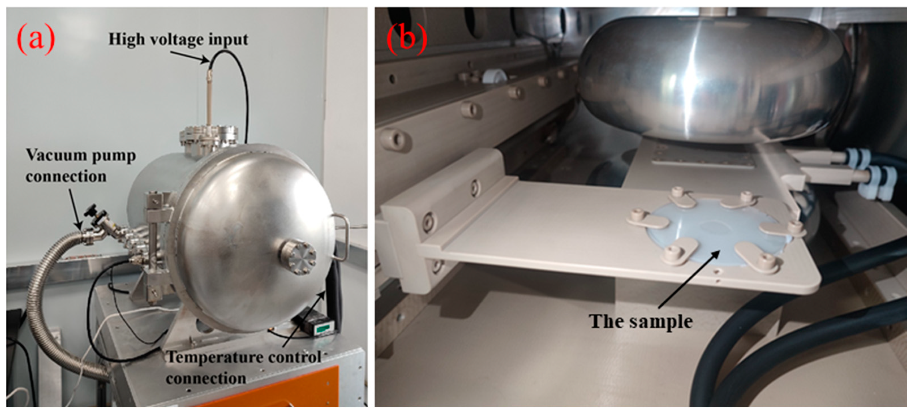
6. Electrode Applications for High-Voltage Sample Environmental Devices

A high-voltage electric field device (Figure 8) was machined and assembled based on the parameters from the simulations. To verify the reliability of the device in terms of the achievable field strength and uniform, power-on tests were performed by adjusting the gap spacing and the power supplied. Detailed information about the design, tests, and scientific applications will be presented separately.

7. Conclusions

The electric field strength and potential distribution of Bruce electrodes with various geometries and chamber diameters were examined based on FEM using ANSYS Maxwell for the development of high-voltage sample environment devices. Three functional sections of the electrode tangentially merge into each other, achieving a large uniform field region where samples will sit along both the electrode surface and the gap axis between the electrodes. The size of the uniform region and field strength highly rely on the gap distance between the electrodes. The edging effect cannot be avoided with the field strength in the sinusoidal region being higher (byabout 1.7%) than that in the uniform plain region, and will be significantly expanded if a chamber is applied. The expansion, however, possesses an exponential decrease as a function of the minimum distance between the electrode edge and the chamber shell, facilitating defining the minimum size of the device if an extremely high voltage is required. The compromise between the edging effect and the chamber size is applicable if the spatial confinement is critical for neutron instruments. This research provides a theoretical basis for the development of high-voltage electric field sample environment devices for in situ SANS or NR measurements.

Author Contributions

G.S.: methodology, investigation and writing—original draft. T.G. methodology and visualization. B.Y. data curation and investigation. X.Y. data curation and writing—review and editing. G.W. conceptualization, funding acquisition, project administration, supervision and writing—review and editing. All authors have read and agreed to the published version of the manuscript.

Funding

This work was supported by the Guangdong Basic and Applied Basic Research Foundation (2021B1515140015), the Natural Science Foundation of Beijing Municipality (Grant No.: 2212051) and the Yunnan Fundamental Research Projects (Grant No. 202201BE070001-038).

Data Availability Statement

The data presented in this study are available on request from the corresponding author.

Acknowledgments

The authors would like to thank Guang Wang and Xiaojing Yang for their technical assistance.

Conflicts of Interest

The authors declare that they have no known competing financial interests or personal relationships that could have appeared to influence the work reported in this paper.

References

  1. Kompatscher, M.; Bär, M.; Hecht, J.; Muheim, C.; Kohlbrecher, J.; Kostorz, G.; Wagner, W. A high-temperature cell for in situ small-angle neutron scattering studies of phase separation in alloys. Nucl. Instrum. Methods Phys. Res. Sect. A Accel. Spectrometers Detect. Assoc. Equip. 2002, 495, 40–47. [Google Scholar] [CrossRef]
  2. Hu, H.; Zhang, C.; Dou, M.; Huang, Z.; Sun, Y.; Ye, F.; Yuan, B.; Bai, B.; Cheng, H.; Yang, S. Experimental and numerical investigation the radiant heating element in neutron scattering furnace. Nucl. Instrum. Methods Phys. Res. Sect. A Accel. Spectrometers Detect. Assoc. Equip. 2023, 1053, 168317. [Google Scholar] [CrossRef]
  3. Kandemir, T.; Wallacher, D.; Hansen, T.; Liss, K.-D.; d’Alnoncourt, R.N.; Schlögl, R.; Behrens, M. In situ neutron diffraction under high pressure—Providing an insight into working catalysts. Nucl. Instrum. Methods Phys. Res. Sect. A Accel. Spectrometers Detect. Assoc. Equip. 2012, 673, 51–55. [Google Scholar] [CrossRef]
  4. Kirichek, O. Sample environment for neutron scattering experiments at ISIS. Neutron News 2019, 30, 14–16. [Google Scholar] [CrossRef]
  5. Bailey, I. A review of sample environments in neutron scattering. Z. Für Krist.-Cryst. Mater. 2003, 218, 84–95. [Google Scholar] [CrossRef]
  6. Usher, T.-M.; Forrester, J.S.; McDonnell, M.; Neuefeind, J.; Page, K.; Peterson, P.F.; Levin, I.; Jones, J.L. Time-of-flight neutron total scattering with applied electric fields: Ex situ and in situ studies of ferroelectric materials. Rev. Sci. Instrum. 2018, 89, 092905. [Google Scholar] [CrossRef]
  7. Koch, C. Experimental evidence for magnetic or electric field effects on phase transformations. Mater. Sci. Eng. A 2000, 287, 213–218. [Google Scholar] [CrossRef]
  8. Xi, Y.; Pozzo, L.D. Electric field directed formation of aligned conjugated polymer fibers. Soft Matter 2017, 13, 3894–3908. [Google Scholar] [CrossRef]
  9. Hanzawa, K.; Sato, H.; Hiramatsu, H.; Kamiya, T.; Hosono, H. Electric field-induced superconducting transition of insulating FeSe thin film at 35 K. Proc. Natl. Acad. Sci. USA 2016, 113, 3986–3990. [Google Scholar] [CrossRef]
  10. Ma, L.; Lei, B.; Wang, N.; Yang, K.; Liu, D.; Meng, F.; Shang, C.; Sun, Z.; Cui, J.; Zhu, C. Electric-field-controlled superconductor–ferromagnetic insulator transition. Sci. Bull. 2019, 64, 653–658. [Google Scholar] [CrossRef]
  11. Shiogai, J.; Ito, Y.; Mitsuhashi, T.; Nojima, T.; Tsukazaki, A. Electric-field-induced superconductivity in electrochemically etched ultrathin FeSe films on SrTiO3 and MgO. Nat. Phys. 2016, 12, 42–46. [Google Scholar] [CrossRef]
  12. Xu, G.; Zhong, Z.; Bing, Y.; Ye, Z.-G.; Shirane, G. Electric-field-induced redistribution of polar nano-regions in a relaxor ferroelectric. Nat. Mater. 2006, 5, 134–140. [Google Scholar] [CrossRef]
  13. Kan, D.; Pálová, L.; Anbusathaiah, V.; Cheng, C.J.; Fujino, S.; Nagarajan, V.; Rabe, K.M.; Takeuchi, I. Universal behavior and electric-field-induced structural transition in rare-earth-substituted BiFeO3. Adv. Funct. Mater. 2010, 20, 1108–1115. [Google Scholar] [CrossRef]
  14. Zhou, J.; Wang, Q.; Sun, Q.; Jena, P.; Chen, X. Electric field enhanced hydrogen storage on polarizable materials substrates. Proc. Natl. Acad. Sci. USA 2010, 107, 2801–2806. [Google Scholar] [CrossRef] [PubMed]
  15. Yue-Hong, Y.; Hong-Ping, X. Theoretical study on the hydrogen storage properties of (MgO)(4) under external electric field. Acta Phys. Sin. 2019, 68, 163601. [Google Scholar] [CrossRef]
  16. Noruzi, K.; Swami, P.; Frejo, L.; Wright, J.; Wong, J.; Grande, D.; Datta-Chaudhuri, T. Effect of uniform capacitively coupled electric fields on matrix metabolism of osteoarthritic cartilage. Bioelectron. Med. 2022, 8, 14. [Google Scholar] [CrossRef] [PubMed]
  17. López-Alonso, B.; Hernáez, A.; Sarnago, H.; Naval, A.; Güemes, A.; Junquera, C.; Burdío, J.M.; Castiella, T.; Monleón, E.; Gracia-Llanes, J. Histopathological and ultrastructural changes after electroporation in pig liver using parallel-plate electrodes and high-performance generator. Sci. Rep. 2019, 9, 2647. [Google Scholar] [CrossRef]
  18. Saunders, L.K.; Yeung, H.-M.; Warren, M.R.; Smith, P.; Gurney, S.; Dodsworth, S.F.; Vitorica-Yrezabal, I.J.; Wilcox, A.; Hathaway, P.V.; Preece, G. An electric field cell for performing in situ single-crystal synchrotron X-ray diffraction. J. Appl. Crystallogr. 2021, 54, 1349–1359. [Google Scholar] [CrossRef]
  19. Vergentev, T.Y.; Dyadkin, V.; Chernyshov, D.Y. In situ cell for X-ray single-crystal diffraction experiment at electric field. J. Surf. Investig. X-Ray Synchrotron Neutron Tech. 2015, 9, 436–441. [Google Scholar] [CrossRef]
  20. Giacomelli, F.C.; da Silveira, N.P.; Nallet, F.; Cernoch, P.; Steinhart, M.; Stepanek, P. Cubic to hexagonal phase transition induced by electric field. Macromolecules 2010, 43, 4261–4267. [Google Scholar] [CrossRef]
  21. Hayward, D.W.; Magro, G.; Hörmann, A.; Prévost, S.; Schweins, R.; Richardson, R.M.; Gradzielski, M. A temperature-controlled electric field sample environment for small-angle neutron scattering experiments. Rev. Sci. Instrum. 2021, 92, 033903. [Google Scholar] [CrossRef] [PubMed]
  22. Harrison, J. A computer study of uniform-field electrodes. Br. J. Appl. Phys. 1967, 18, 1617. [Google Scholar] [CrossRef]
  23. Luo, D.; Hui, D.-D.; Wen, W.-L.; Li, L.-L.; Xin, L.-W.; Zhong, Z.-Y.; Ji, C.; Chen, P.; He, K.; Wang, X.; et al. Design of a femtosecond electron diffractometer with adjustable gaps. Acta Phys. Sin. 2020, 69, 052901. [Google Scholar] [CrossRef]
  24. Rogowski, W. Die elektrische Festigkeit am Rande des Plattenkondensators: Ein Beitrag zur Theorie der Funkenstrecken und Durchführungen. Arch. Für Elektrotechnik 1923, 12, 1–15. [Google Scholar] [CrossRef]
  25. Bruce, F. Calibration of uniform-field spark-gaps for high-voltage measurement at power frequencies. J. Inst. Electr. Eng.-Part II Power Eng. 1947, 94, 138–149. [Google Scholar] [CrossRef]
  26. Sant’Anna, G.M.; Roveri, D.S.; Bertan, H.H.; Mologni, J.F.; Braga, E.S.; Alves, M.A.R. Analysis of the electric field behavior in the vicinity of a triple junction, using finite elements method computational simulations. J. Electrost. 2015, 74, 96–101. [Google Scholar] [CrossRef]
  27. Naik, S.; Bag, B.; Chandrasekaran, K. Electrical Field Analysis of Different Structure Conductors using FEM. In Proceedings of the 2021 International Conference on Advances in Electrical, Computing, Communication and Sustainable Technologies (ICAECT), Bhilai, India, 19–20 February 2021; pp. 1–5. [Google Scholar] [CrossRef]
  28. Amin, N.; Ishak, M.; Hamid, M.; Abd Rahman, M. Partial discharge investigation on palm oil using needle—Plane electrode configuration and electric field distribution using ANSYS Maxwell. In Proceedings of the 2017 International Conference on High Voltage Engineering and Power Systems (ICHVEPS), Denpasar, Indonesia, 2–5 October 2017; pp. 440–445. [Google Scholar] [CrossRef]
  29. Wang, M.; Wang, Z.; Shi, Z.; Dong, C.; Liu, W.; Tao, L. Optimization simulation of electric field of electrode leads for electrical desalination based on finite element analysis. Mod. Chem. Ind. 2022, 51, 646–650. (In Chinese) [Google Scholar] [CrossRef]
  30. Zhang, T.; Li, M.; Yang, B. Finite element analysis and simulation research on three-dimensional electric field of capacitive angular displacement sensor. Comput. Simul. 2003, 20, 45–47. [Google Scholar] [CrossRef]
  31. Sima, W.; Yang, Q.; Sun, C.; Guo, F. Potential and electric-field calculation along an ice-covered composite insulator with finite-element method. IEE Proc.-Gener. Transm. Distrib. 2006, 153, 343–349. [Google Scholar] [CrossRef]
  32. Wang, Z.; Quan, Y. Engineering Electromagnetic; Tsinghua University Press: Beijing, China, 2021; p. 383. Available online: https://www.tup.tsinghua.edu.cn (accessed on 7 February 2024).
  33. Trinh, N.G. Electrode design for testing in uniform field gaps. IEEE Trans. Power Appar. Syst. 1980, PAS-99, 1235–1242. [Google Scholar] [CrossRef]
Figure 1. Sectional schematic diagram of the Bruce electrode [32].
Instruments 08 00026 g001
Figure 2. SolidWorks 3D modeling (Left), ANSYS Maxwell 2D model (Middle), and the calculation domain (Right) for the simulation of electrodes.
Instruments 08 00026 g002
Figure 3. Electric field vectors between and around the electrodes.
Instruments 08 00026 g003
Figure 4. Field strength distribution of (a) Model A, (b) Model B, (c) Model C, (d) Model D, and (e) Model E, and (f) the variation in field strength along the black line in Model E for all five models.
Instruments 08 00026 g004
Figure 5. (a) Selected positions of Model E (39 mm gap spacing) for field strength comparisons; (b) field strength along the surface of the top electrode and the center of the gap between the electrodes, respectively; (c) field strength along the gap axis (from top to bottom) in various sections; and (d) the zoomed version of (c).
Instruments 08 00026 g005
Figure 6. Field strength distribution between the electrodes of Model E when a chamber with a diameter (minimum distance between upper electrode edge and chamber shell) of (a) 450 (70), (b) 500 (95), (c) 550 (120), (d) 600 (145), and (e) 650 (170) mm is applied, and (f) the strength curves of the electrodes obtained along the black line in Figure 4e.
Instruments 08 00026 g006
Figure 7. (a) Field intensity distribution along the line on the upper electrode surface shown in Figure 5a and (b) plot of maximum field strength as a function of the minimum distance between upper electrode edge and chamber shell.
Instruments 08 00026 g007
Figure 8. The layout of the device outside (a) and inside (b).
Instruments 08 00026 g008
Table 1. Specifications of Bruce electrode geometries. Notes: R0: Radius of the plane area; α: Characteristic angle of the sinusoidal section; A: Distance from the plane section to the center of the circle section; D: Overall diameter of electrodes; T: Electrode thickness; Re: Circle radius; d: Electrode nominal gap spacing.
ModelR0/mmα/°A/mmD/mmT/mmRe/mmd/mm
A404015130231011.5
B4045151372813.514
C405019162452222.5
D405520184603230
E406020208784439
Table 2. Parameters of materials for FEM modeling.
ParametersAnode
(Aluminum)
Cathode
(Aluminum)
VacuumElectrode Support
(PEEK)
Vacuum Chamber
(Stainless Steel)
Relative permittivity ( ε r )1113.11
Conductivity (Siemens/m)38 × 10638 × 106010 × 10711 × 105
Disclaimer/Publisher’s Note: The statements, opinions and data contained in all publications are solely those of the individual author(s) and contributor(s) and not of MDPI and/or the editor(s). MDPI and/or the editor(s) disclaim responsibility for any injury to people or property resulting from any ideas, methods, instructions or products referred to in the content.

