Article

Inkjet-Printed Interdigitated Capacitors for Sensing Applications: Temperature-Dependent Electrical Characterization at Cryogenic Temperatures down to 20 K

1
Department of Engineering, University of Messina, 98166 Messina, Italy
2
Department of Industrial, Electronic and Mechanical Engineering, Roma Tre University, 00146 Roma, Italy
3
BIOMORF Department, University of Messina, 98125 Messina, Italy
*
Author to whom correspondence should be addressed.
Instruments 2023, 7(3), 20; https://doi.org/10.3390/instruments7030020
Submission received: 17 May 2023 / Revised: 16 July 2023 / Accepted: 17 July 2023 / Published: 19 July 2023

Abstract

:
Microwave transducers are widely used for sensing applications in areas such as gas sensing and microfluidics. Inkjet printing technology has been proposed as a promising method for fabricating such devices due to its capability to produce complex patterns and geometries with high precision. In this work, the temperature-dependent electrical properties of an inkjet-printed single-port interdigitated capacitor (IDC) were investigated at cryogenic temperatures down to 20 K. The IDC was designed and fabricated using inkjet printing technology, while its reflection coefficient was measured using a vector network analyzer in a cryogenic measurement setup and then transformed into the corresponding admittance. The resonant frequency and quality factor (Q-factor) of the IDC were extracted as functions of the temperature and their sensitivity was evaluated. The results showed that the resonant frequency shifted to higher frequencies as the temperature was reduced, while the Q-factor increased as the temperature decreased. The trends and observations in the temperature-dependent electrical properties of the IDC are discussed and analyzed in this paper, and are expected to be useful in future advancement of the design and optimization of inkjet-printed microwave transducers for sensing applications and cryogenic electronics.

1. Introduction

In recent years, microwave transducers have gained widespread use in various fields, including sensing applications [1,2,3], dielectric materials characterization [4,5,6], microfluidics [7,8,9], and metrological applications [10,11,12]. The high sensitivity and fast response time of these devices make them suitable for measuring small changes in physical, chemical, and biological parameters. Microwave transducers designed in microstrip or coplanar technology have been widely adopted due to their features of easy fabrication, low cost, and low power requirements [13]. These devices inherit compatibility with wireless technology, as they operate in radio frequency bands, and offer the advantage of contactless measurements, which are highly desirable or even essential in various sensing applications [14,15,16]. Various geometries for microwave transducers have been proposed in the literature, such as disk resonators [17], ring resonators [18], split-ring resonators [19], spirals [1], rectangular patches [20], and interdigitated capacitors (IDCs) [3], with each geometry offering specific advantages for particular applications. Among the different geometries, IDCs have been widely studied and employed in sensing applications from low frequencies to the microwave range [3,21,22,23].
The concept of interdigital electrodes was first introduced by Nikola Tesla in 1891 [24], when he used parallel rectangular plates known as fingers to increase the total capacitance of an electrical condenser. This principle is used today in the fabrication of modern capacitors [25]. The theoretical expression for the estimation of the capacitance between coplanar strips was introduced in 1924 [26]. However, it was not until the 1960s that interdigital electrodes started to be extensively used for sensing applications [25]. Their simple design and ease of fabrication using such different technologies as screen printing, computer numerical control (CNC) micromachining, and inkjet printing, are among of the key advantages of IDCs.
The small size of IDCs makes them suitable for sensing applications and integration into microfluidic devices. In microfluidic systems, IDCs can be used as sensing elements to monitor the conductivity of the liquid under test or its dielectric properties, detecting and quantifying chemical and biological species [21,22,27,28]. These features make IDCs suitable for medical diagnostics and lab-on-a-chip applications [8,29].
In gas sensing, IDCs are frequently combined with a sensing material with dielectric properties that change in the presence of the target gas [3]. The surface of the IDC is coated with a sensing layer that reacts with the gas, causing changes in the electrical properties of the material, such as its effective complex permittivity. These changes can then be detected by the IDC as a variation in the total equivalent capacitance and this value can be related to the gas target concentration through a proper calibration procedure. IDCs have been employed in the microwave range to develop gas sensors for various gases, including oxygen [3], ammonia [30], and ethanol [31], among others.
Inkjet printing technology has emerged as a cost-effective and high-resolution alternative to more traditional fabrication techniques. It offers a contactless, maskless, and flexible approach to the deposition of conductive ink on substrates. Inkjet printing has been used in a wide range of applications, such as flexible electronics [32,33], on-paper devices [34], and microwave transducers [35]; however, one of the major limitations of this technology is related to the properties of the ink and how they can vary with time or operating conditions. For instance, the performance of inkjet-printed devices can be affected by factors such as the relative humidity or temperature [36], which can result in changes to the ink properties and lead to decreased device performance. Despite this issue, few studies have been conducted on the performance of inkjet-printed microwave transducers under extreme conditions, particularly at cryogenic temperatures. In this context, studying the behavior of inkjet-printed microwave transducers over a range of operating temperatures, particularly at cryogenic temperatures, can provide valuable insights into the performance and reliability of such devices. Moreover, a thorough understanding of the temperature-dependent electrical properties of microwave transducers can be helpful for optimization of the design and performance of high-performance microwave sensors.
In this study, we have focused on investigating the temperature-dependent electrical properties of an inkjet-printed interdigitated capacitor over a wide temperature range from 20 K to 300 K. The substrate material used for fabrication of the IDC was glass-reinforced epoxy laminate (FR4), which was characterized in terms of its electromagnetic properties. The obtained characterization results were used for the design of the prototype by employing computer-aided design (CAD) simulation software. The IDC prototype was fabricated by printing it onto the FR4 substrate using a Voltera V-One printer along with a commercial conductive ink, the Conductor 2 ink produced by Voltera [37]. A single-port IDC was designed using coplanar technology and its electrical properties were evaluated using a vector network analyzer (VNA), for which the device was placed inside a cryogenic measurement system. The aim of the study was to provide a more comprehensive understanding of the electrical behavior of inkjet-printed IDCs at cryogenic temperatures.
The rest of the article is organized into four sections: Section 2 below comprises three subsections detailing the characterization of the FR4 material, the design and fabrication of the IDC prototype, and the cryogenic test setup; Section 3 outlines the main results obtained from the tests; then the article concludes with Section 4, which provides a summary of the main findings and their significance.

2. Materials and Methods

This section of the paper provides a detailed account of the materials and methods employed to investigate the temperature-dependent electrical properties of the inkjet-printed interdigitated capacitor. The section is divided into three subsections, each of which outlines a specific aspect of the investigation. The first subsection focuses on the characterization of the FR4 material used as a substrate for the IDC under test. The dielectric constant and loss tangent of the FR4 material were determined through experimental measurements, and were subsequently used in the device design process. This process is discussed in the second subsection, which provides a comprehensive description of the IDC prototype, including its geometric parameters and fabrication process through inkjet printing technique. The design of the IDC prototype was carried out using Matlab software; the details of this design process are included in this subsection as well. The third and final subsection provides a detailed description of the cryogenic measurement system used to perform the temperature-dependent electrical measurements of the IDC prototype. The measurement system was designed to operate over a wide temperature range and equipped with a VNA to measure the electrical properties of the IDC at different operating conditions.

2.1. Material Characterization

The initial step in the IDC design process involves the characterization of the electromagnetic properties of the substrate material being used. In this case, it was a commercial FR4 provided by the Voltera company. The dielectric constant values of FR4 substrates differ significantly depending on the material’s anisotropy and resin content [38]. Therefore, direct measurement is necessary for an appropriate device simulation. The response of a dielectric material to electromagnetic fields is defined by the complex dielectric permittivity  ε 0 ε ˜ = ε 0 ( ε i ε ) , where  ε 0  is the dielectric constant of vacuum  ε = Re ( ε ˜ ) ε = Im ( ε ˜ ) , the ratio  tan δ = ε / ε  is known as the loss tangent, and  i = 1  [39]. Therefore, in order to design the resonator geometry parameters accurately it is essential to measure the complex dielectric permittivity of the FR4 substrate used for the IDC substrate.
Microwave measurement techniques employed for material characterization can be categorized into two main groups [40], resonant and non-resonant. The former is well known for its high sensitivity, while the latter, although possessing lower sensitivity and accuracy, provides the significant benefit of being wideband [40]. At the operational frequencies of the designed IDC, the dielectric characteristics of the FR4 are only slightly frequency-dependent [41]; thus, the wideband nature of transmission/reflection measurement techniques does not offer a significant advantage. In contrast, the high sensitivity of resonant methods can be particularly useful for achieving accurate IDC design. Therefore, a dielectric-loaded resonator was exploited to characterize the FR4 substrate, as shown in [6,42] and depicted in Figure 1.
The measurement technique used in this work is known as the volume perturbation technique [40]. In this method, a portion of the internal volume of an electromagnetic resonant structure is first replaced with a reference material and then with the material being investigated. By examining the variation in the quality factor Q and resonance frequency  f 0 , it is possible to estimate the electromagnetic properties of the unknown material [40]. Air is utilized as the reference material here due to its dielectric constant being approximately  ε ˜ 1 i 0 . It has been demonstrated in previous studies [6,40,42] that  Δ f 0  is proportional to  ε , while  Δ ( Q 1 )  is proportional to the loss tangent  tan δ . Here,  Δ x  indicates the variation in the parameter x with respect to a reference value (in this case, air).
To avoid a significant reduction in Q and resulting loss of sensitivity due to expected large losses of FR4, only a small volume of the resonator was replaced with this material. The optimization of the sample volume with respect to its expected electromagnetic properties is discussed in detail in [42]. In this study, an FR4 fragment with dimensions  15.0 × 15.0 × 1.6 mm 3  was loaded into the resonator, as shown in Figure 1. For evaluation of the measurement repeatability, the reflection and transmission scattering (S-) parameters of the resonator were measured twenty times, with the sample being dismounted for each measurement. Q and  f 0  were determined by fitting the acquired S-parameters using the method described in [43]. It was determined that a single measurement per mounting was sufficient, as a statistical analysis of multiple measurements indicated that the uncertainties on Q and  f 0  were comparable to those obtained through the fitting procedure and analyzing the fit residuals from a single measurement [43].
To obtain the reference measurement, we replaced the same volume of the FR4 sample with air. In this configuration, a ring with the same thickness as the sample under investigation was printed and inserted into the resonator instead of the sample itself. This allowed the resonator geometry to be maintained while introducing a controlled volume of air. Using the FR4 sample, a quality factor of  Q s a m p l e = 2413.8 ( 17 )  and a resonance frequency of  f 0 , s a m p l e = 12.381122 ( 21 )  GHz were obtained, where the values in parentheses represent the numerical value of the experimental standard deviations,  s ( Q s a m p l e )  and  s ( f 0 , s a m p l e ) , respectively, for the corresponding last digits of the reported results. The twenty repeated measurements with the air reference sample resulted in a quality factor of  Q a i r = 4998 ( 13 )  and a resonance frequency of  f 0 , a i r = 12.434475 ( 15 )  GHz.
The relative change in resonance frequency ( Δ f 0 / f 0 , a i r = ( f 0 , s a m p l e f 0 , a i r ) / f 0 , a i r ) was compared with the calibration curves of dielectric permittivity ( ε ( Δ f 0 / f 0 , a i r ) ) and  η ( Δ f 0 / f 0 , a i r ) , with  η  being the sample filling factor [40] obtained through electromagnetic simulations of the resonating structure [42]. The calibration curves shown in Figure 2 were used to determine  ε  and  η . The loss tangent ( tan δ ) was then calculated as  tan δ Δ ( Q 1 ) / η  as described in [42].
The FR4 substrate under analysis yielded  ε = 4.75 ( 8 )  and  tan δ = 1.73 ( 6 ) × 10 2 , which are consistent with values reported in the literature [44]. The reported standard uncertainties were evaluated by propagating the distribution of simulated and measured quantities using the Monte Carlo method in compliance with [45,46]. The simulated  f 0  and  η  were assumed to have a normal distribution with 1% relative standard deviation. In each trial of the Monte Carlo simulation, the calibration curves  ε ( Δ f 0 / f 0 , a i r )  and  η ( Δ f 0 / f 0 , a i r )  were re-evaluated and fitted with a second-order polynomial, providing the uncertainties on the fitting parameters reported in the caption of Figure 2. The measured  f 0 , s a m p l e  and  f 0 , a i r  and their standard deviations allowed  ε  and  η  (as well as their uncertainties) to be obtained, from which  tan δ  (and its uncertainty) was calculated using the measured Q and  s ( Q ) . In all,  10 6  Monte Carlo trials were performed [45].

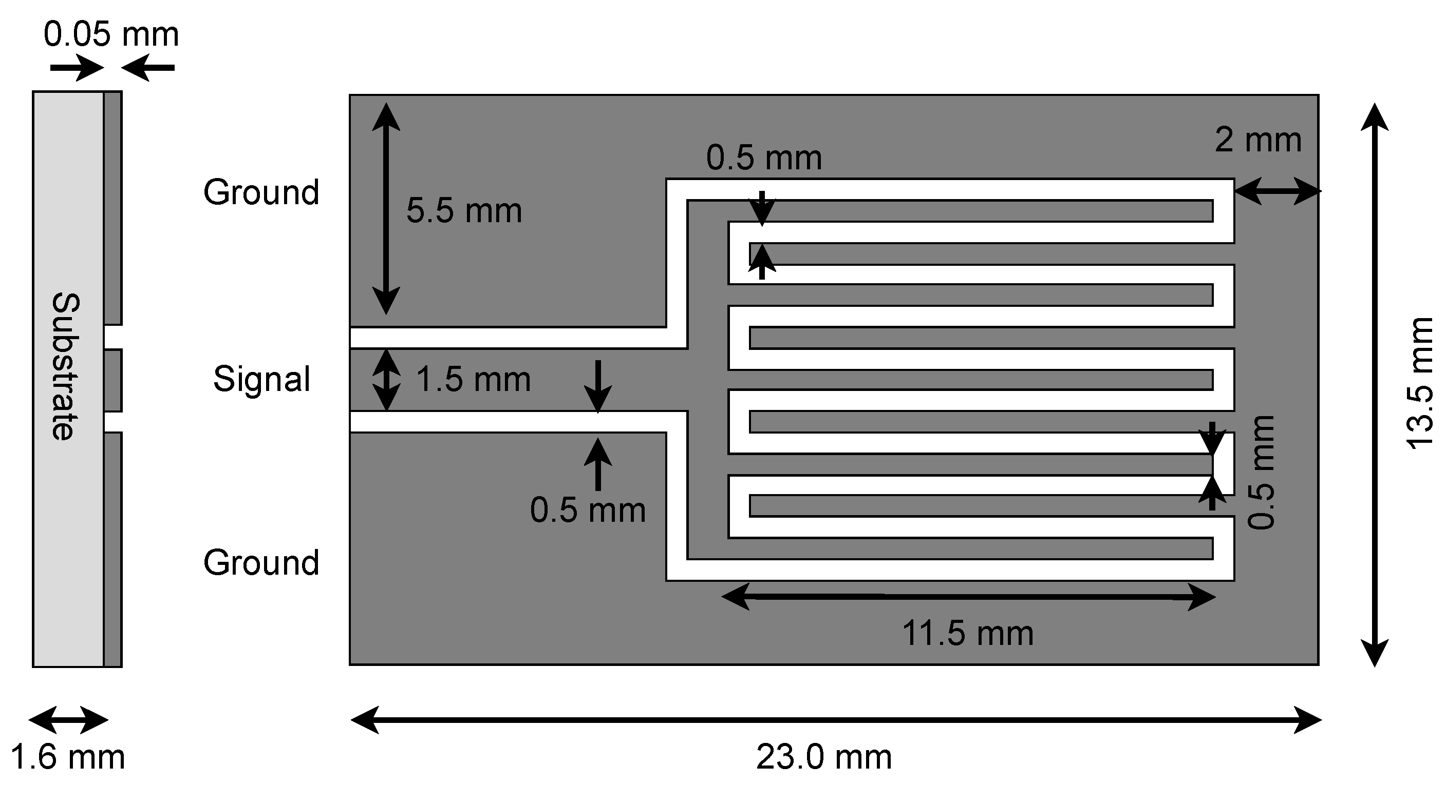
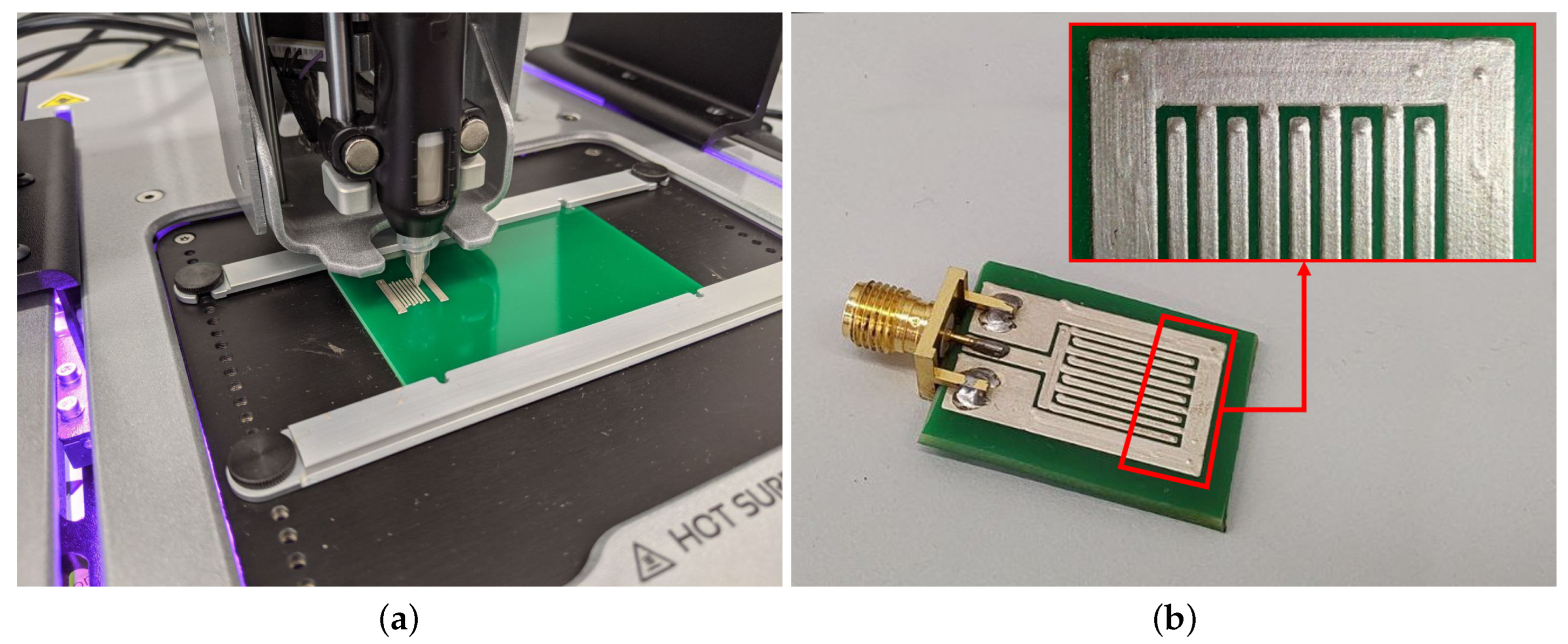
2.2. Inkjet Printed Interdigitated Capacitor: Design and Fabrication

The device under investigation is a one-port coplanar interdigitated capacitor. The design was carried out using MATLAB as a computer-aided design tool. In particular, the Antenna toolbox was used for accurate 3D modeling of the device in order to simulate its electrical response over a frequency range spanning from 100 MHz to 6 GHz. The device was made up of a 1.6-mm-thick FR4 substrate surrounded by a conductive layer. The material properties for the FR4 substrate were set according to the results obtained by the material characterization described in the previous subsection ( ε r  = 4.75;  tan δ  = 0.0173), while the conductive layer properties were set according to the nominal specification of the conductive ink used, i.e., a nominal thickness of 50 µm and a nominal resistivity of  1.265 × 10 7 Ω · m [37].
A 2d drawing of the device is shown in Figure 3. The length, width, and spacing of the fingers are 11.5 mm, 0.5 mm, and 0.5 mm, respectively, while the coplanar feedline’s slot, signal, and finite ground widths are 0.5 mm, 1.5 mm, and 5.5 mm, respectively. The device geometry was selected based on the printer’s resolution (about 225 µm for the selected ink) and need to maintain an overall size less than 1 inch square, i.e.,  2.54 × 2.54  mm 2 . Moreover, the IDC geometry was tuned by means of computer simulations in order to ensure a first resonance at about 1 GHz for the potential use of the IDC in sensing applications [47].
The Voltera V-One inkjet printing machine was used to fabricate the device. This printer is based on direct ink writing (DIW) dispensing technology with an open-loop ink pressure control. It allows tracks with a minimum width of 0.2 mm to be printed, and its resolution is 10 µm × 10 µm × 1 µm, for the x, y, and z axes, respectively. A silver-based conductive ink, “Conductor 2” by Voltera [37], was deposited on the FR4 substrate to create the IDC pattern selected during the design process. The main properties of the employed ink are summarized in Table 1.
The printing process can introduce imperfections if the printer setup is not properly optimized. The best setup parameters depend on several factors, including the properties of the conductive ink (such as density and viscosity), the pressure at which the ink is ejected, the nozzle dimensions, the substrate used (including planarity and roughness), and the device geometry. To ensure high-quality printing results and minimize non-uniformity in the IDC geometry, a calibration procedure was performed before the printing process to properly set all the printer parameters. After the conductive ink had been deposited on the FR4 substrate the prototype was cured in an oven at 200 °C for 30 min. The curing process is crucial, as it triggers the chemical reactions in the ink that allow the metallic particles to fuse together to form a conductive matrix. According to the Voltera FAQ webpage [48], the cured ink exhibits properties similar to standard copper up to 5 GHz. As the last fabrication step, the board was polished, cleaned with isopropyl alcohol, and a sub-miniature version A (SMA) connector was soldered to the end of the coplanar feedline to allow for connection with the VNA used for device characterization. To ensure the best results, in compliance with the manufacturer’s recommendation [37] a soldering temperature of approximately 180 °C was used. Figure 4 shows a photo of the completed IDC prototype.
In this work, the device was characterized in terms of the admittance parameter Y, which was calculated from the reflection coefficient (i.e.,  S 11 ) measured with the VNA and converted using the appropriate formula [49].
Figure 5 presents a comparison of the simulated and measured admittance comprising both the real and imaginary parts across a frequency range spanning from 100 MHz to 6 GHz. The plot exhibits multiple resonances wherein the real part of the admittance reaches a local maximum while the imaginary part is null. Despite a slight frequency shift of approximately 200 MHz towards the lower frequencies in the fabricated prototype, the measured results are in good agreement with the simulations. This deviation can be attributed to inevitable fabrication tolerances and trace spread after printing.
To evaluate the reproducibility of IDC fabrication, three samples were printed on an FR4 substrate using the same Voltera V-One printer, each after separately performing the printer calibration procedure. The results in terms of admittance were then compared, as shown in Figure 6. As can be seen, the comparison revealed variations among the samples in the first and second resonance. The reproducibility was evaluated in terms of standard deviation, which was found to be 16 MHz and 33 MHz for the first and second resonances, respectively. These results indicate that the fabrication process was consistent and reproducible, with only relatively small variations observed between the different samples. Furthermore, the results demonstrate the effectiveness of the printer calibration procedure in minimizing variations during the printing process.

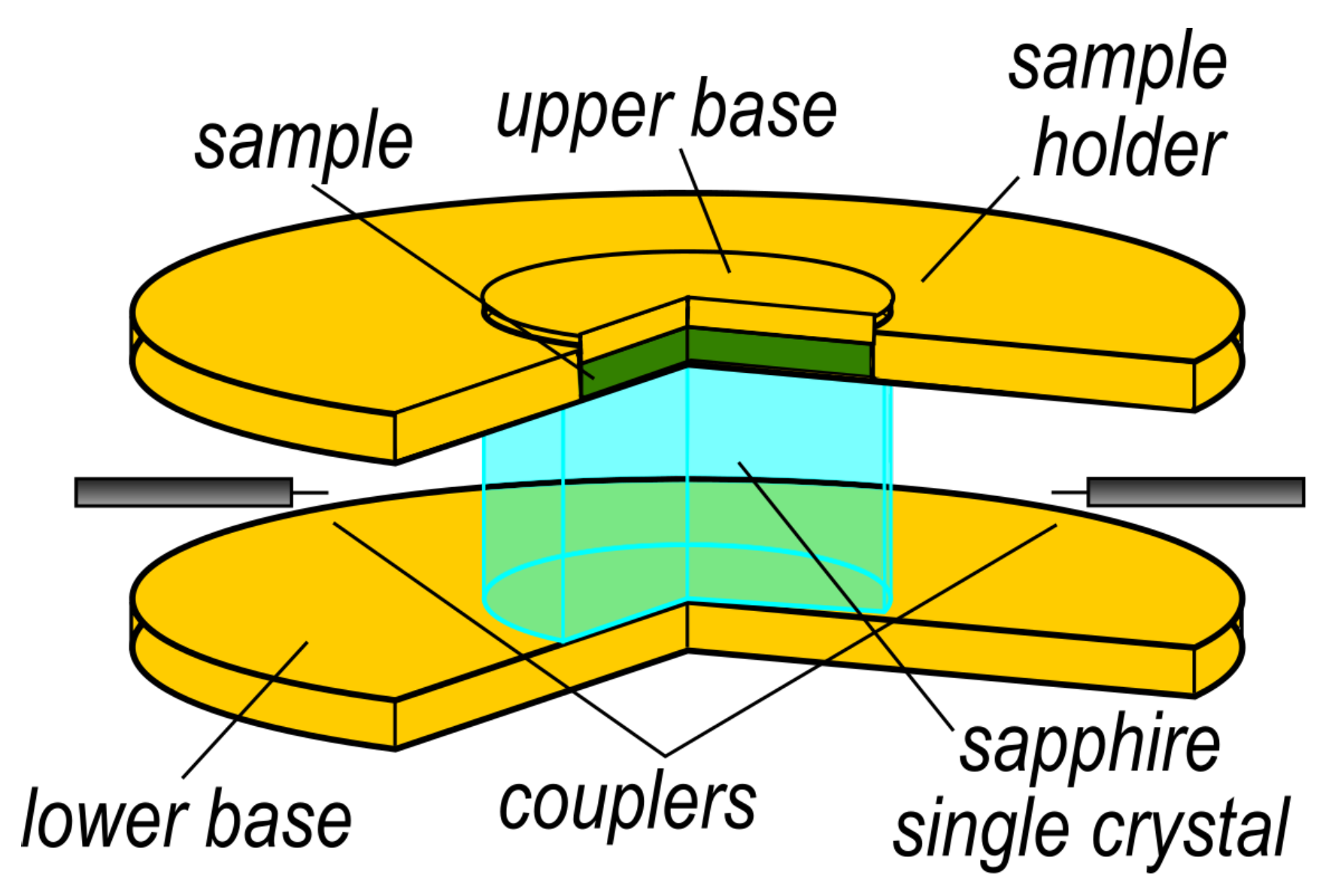
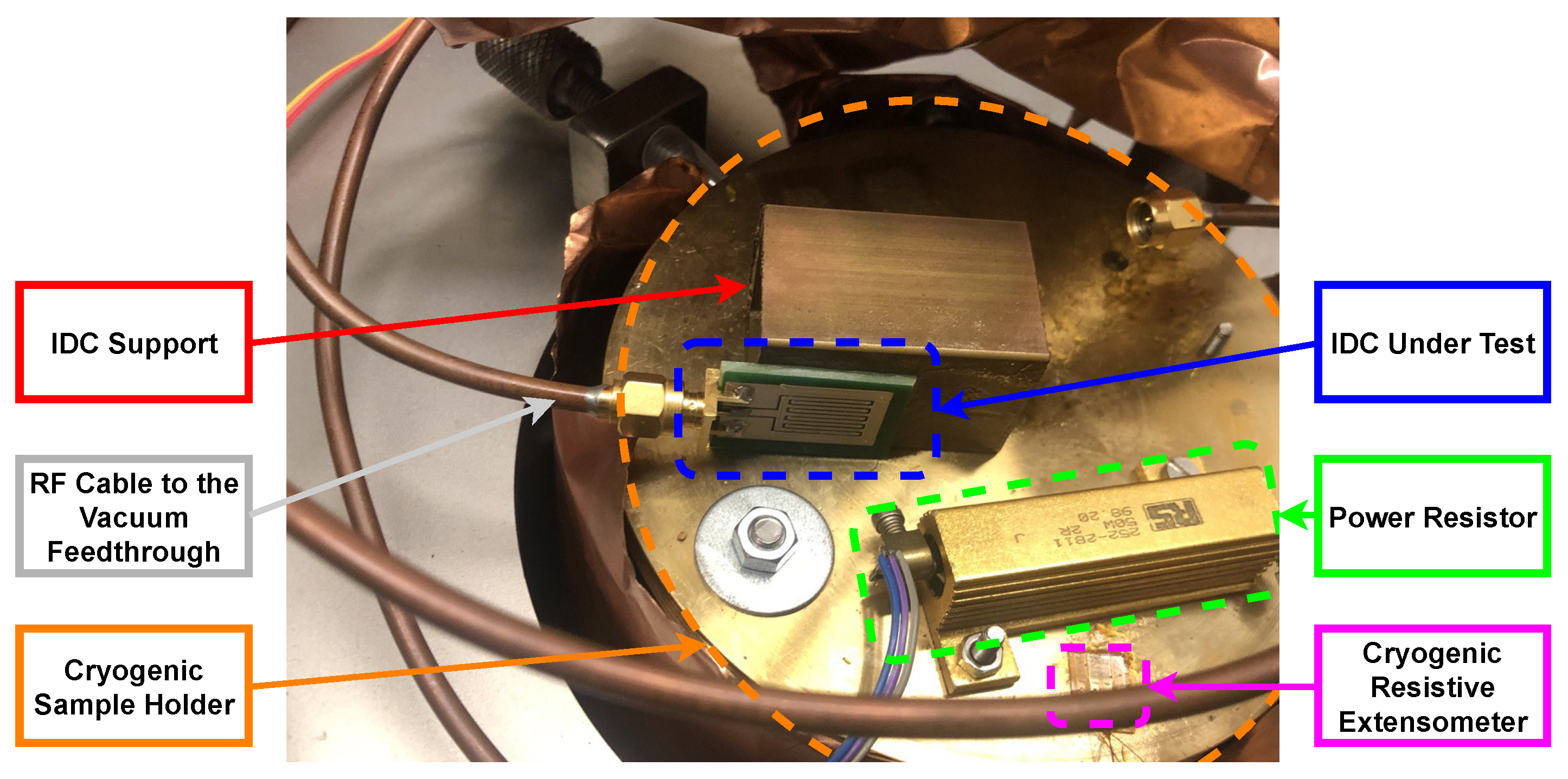
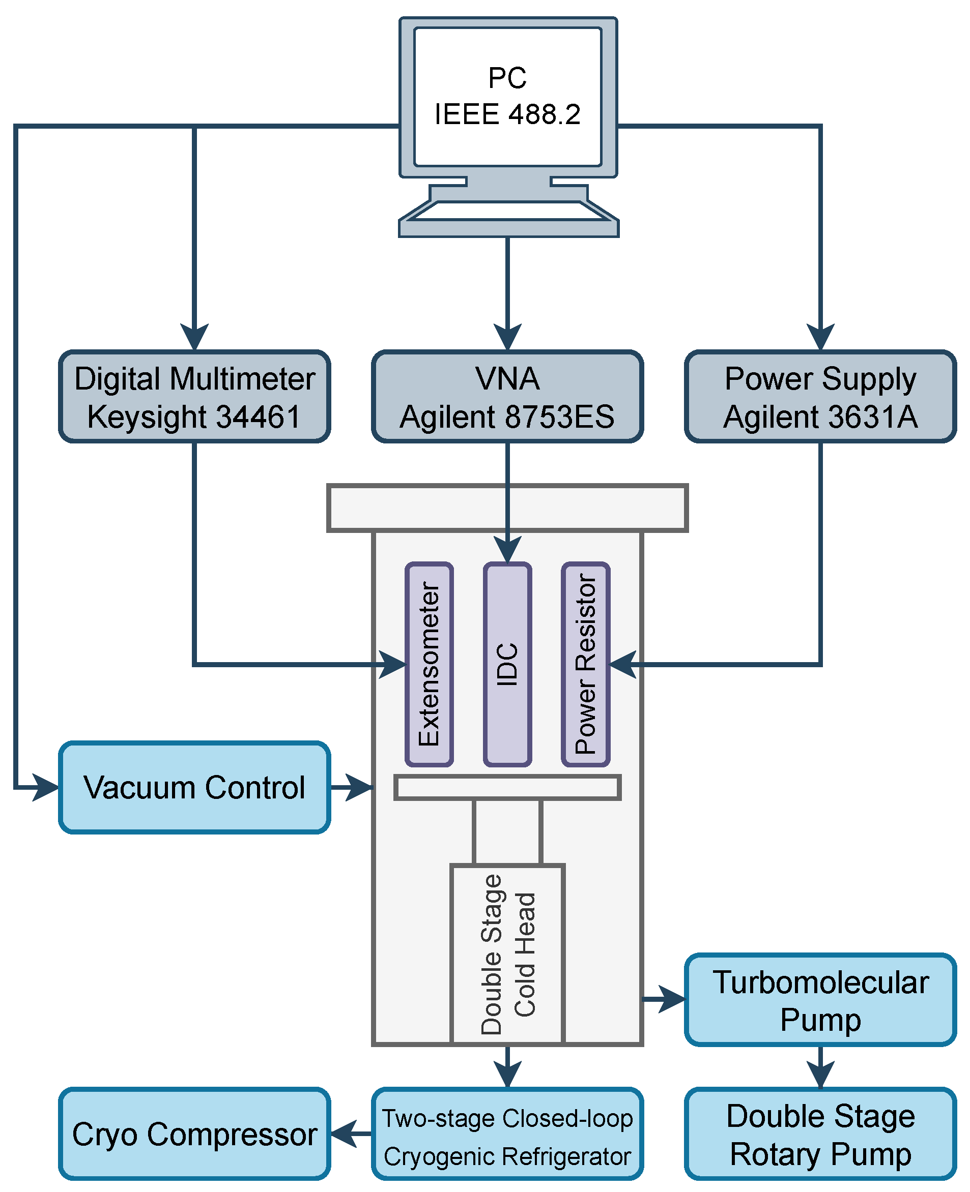
2.3. Experimental Setup
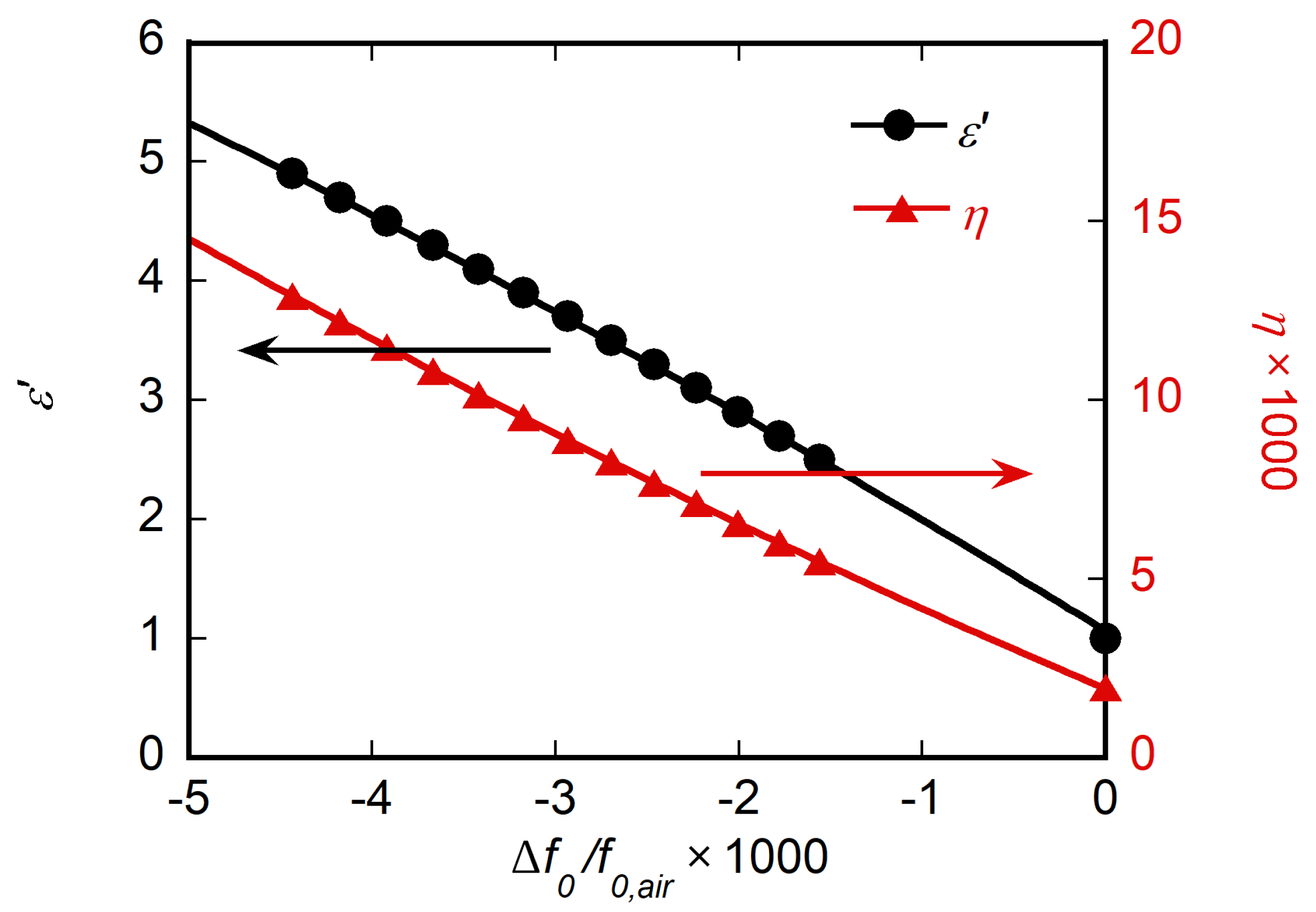
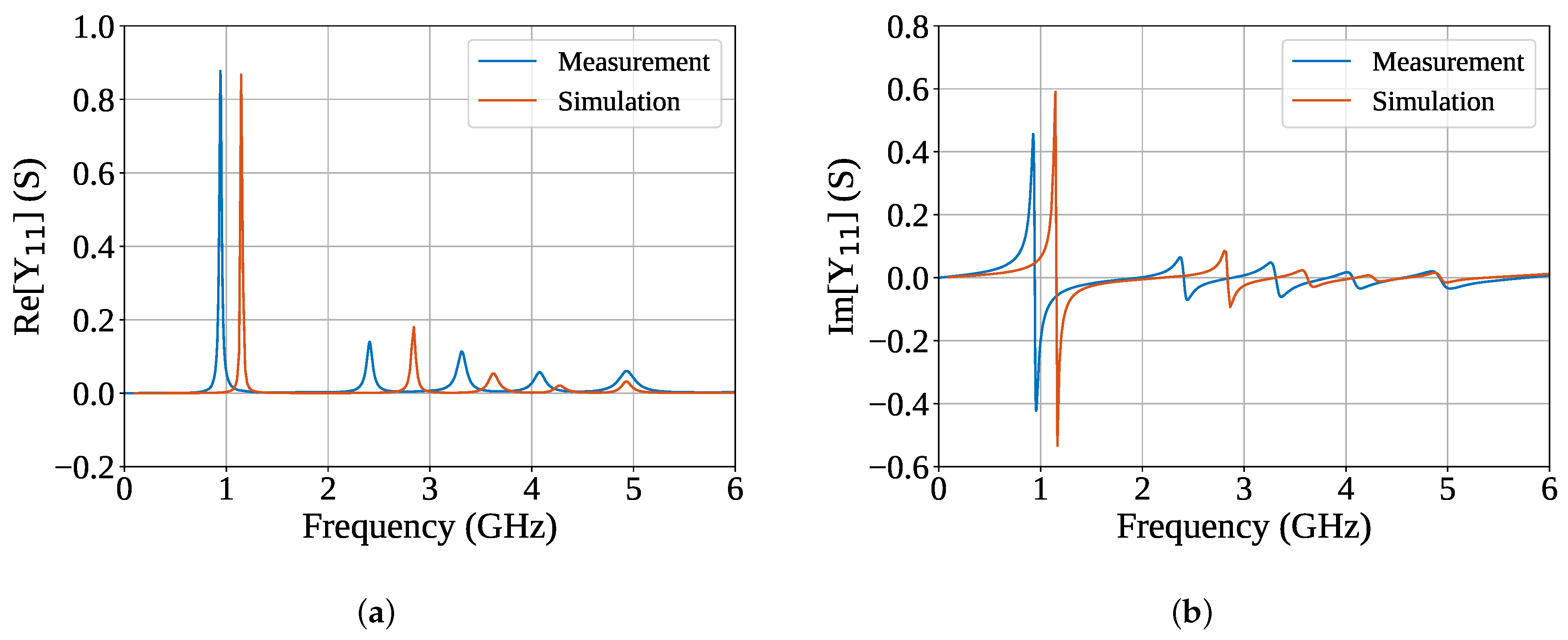
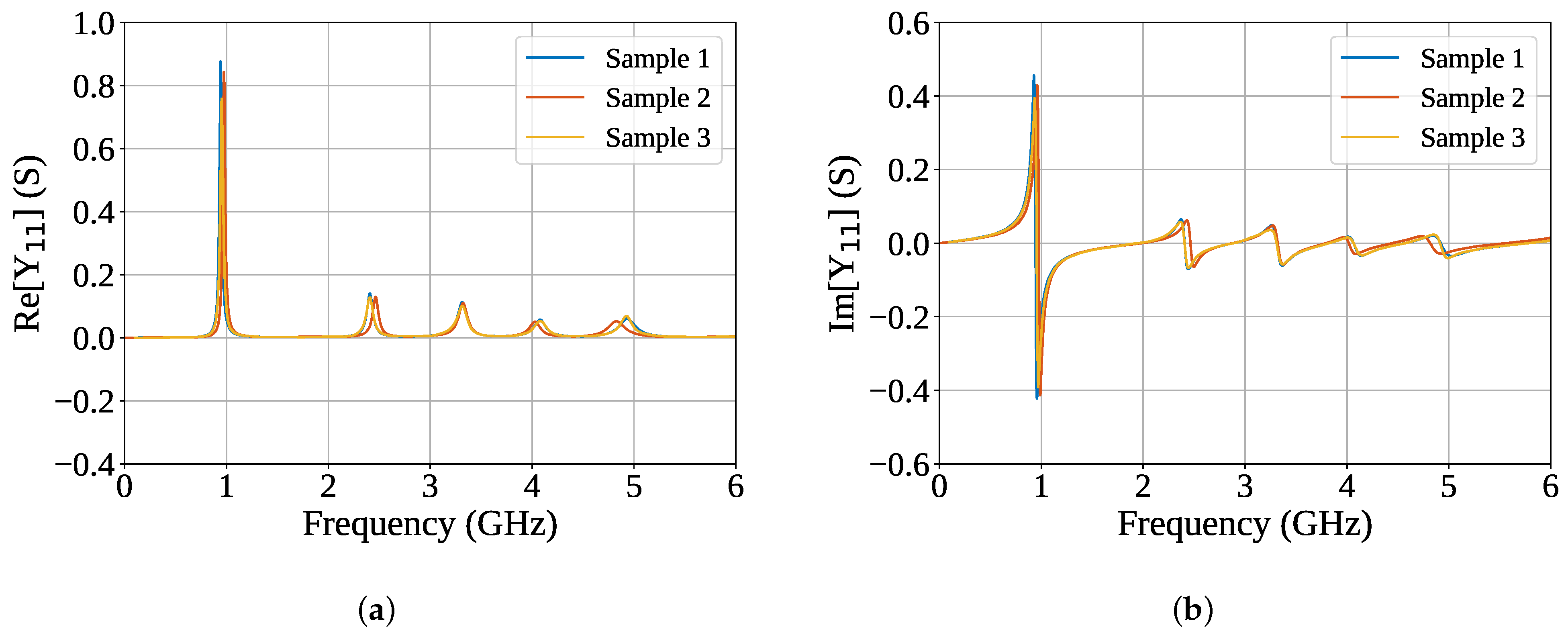
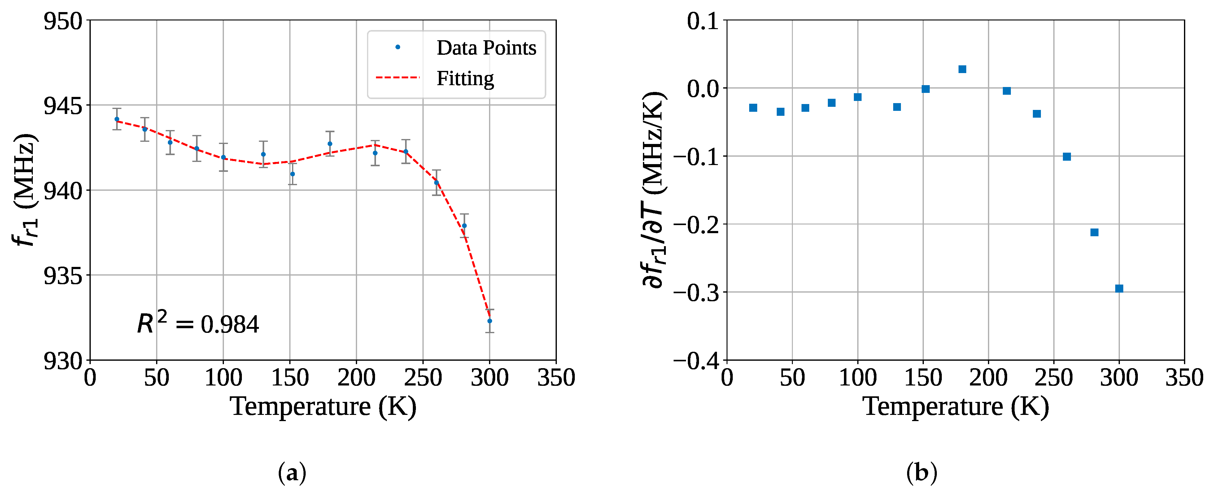
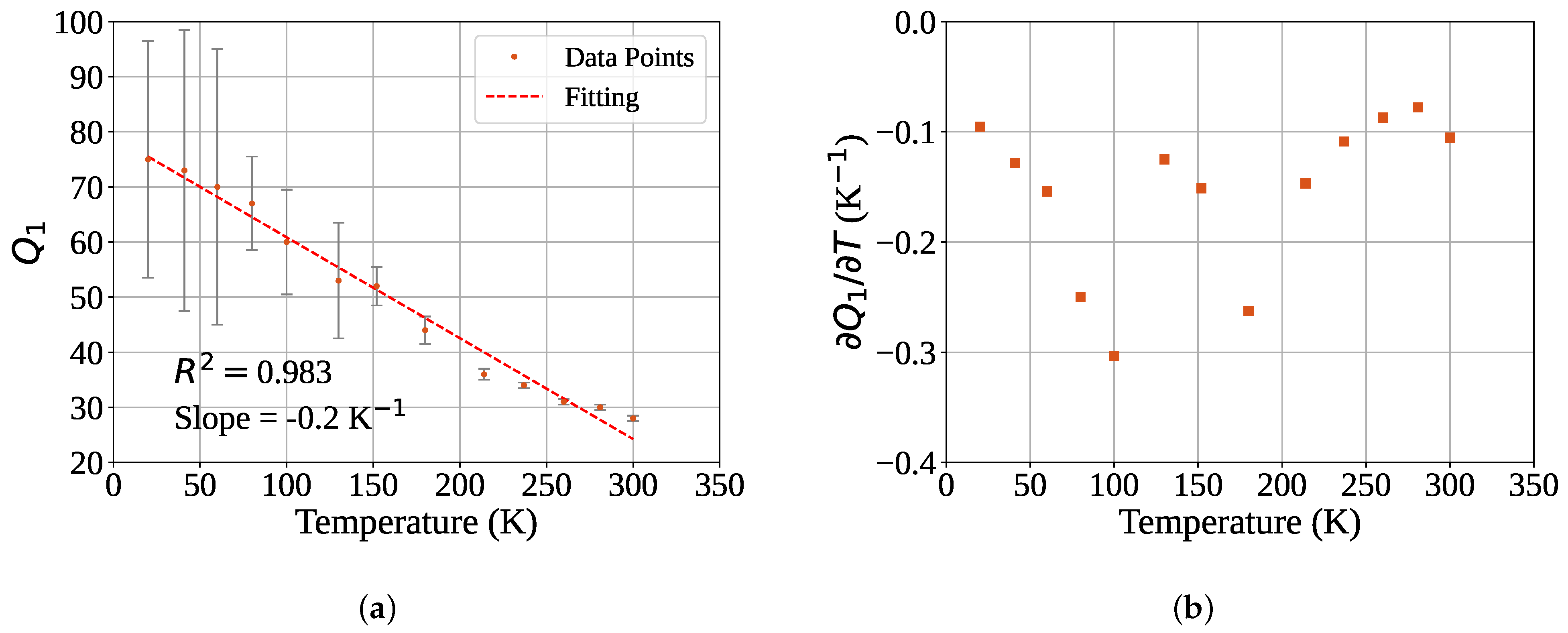
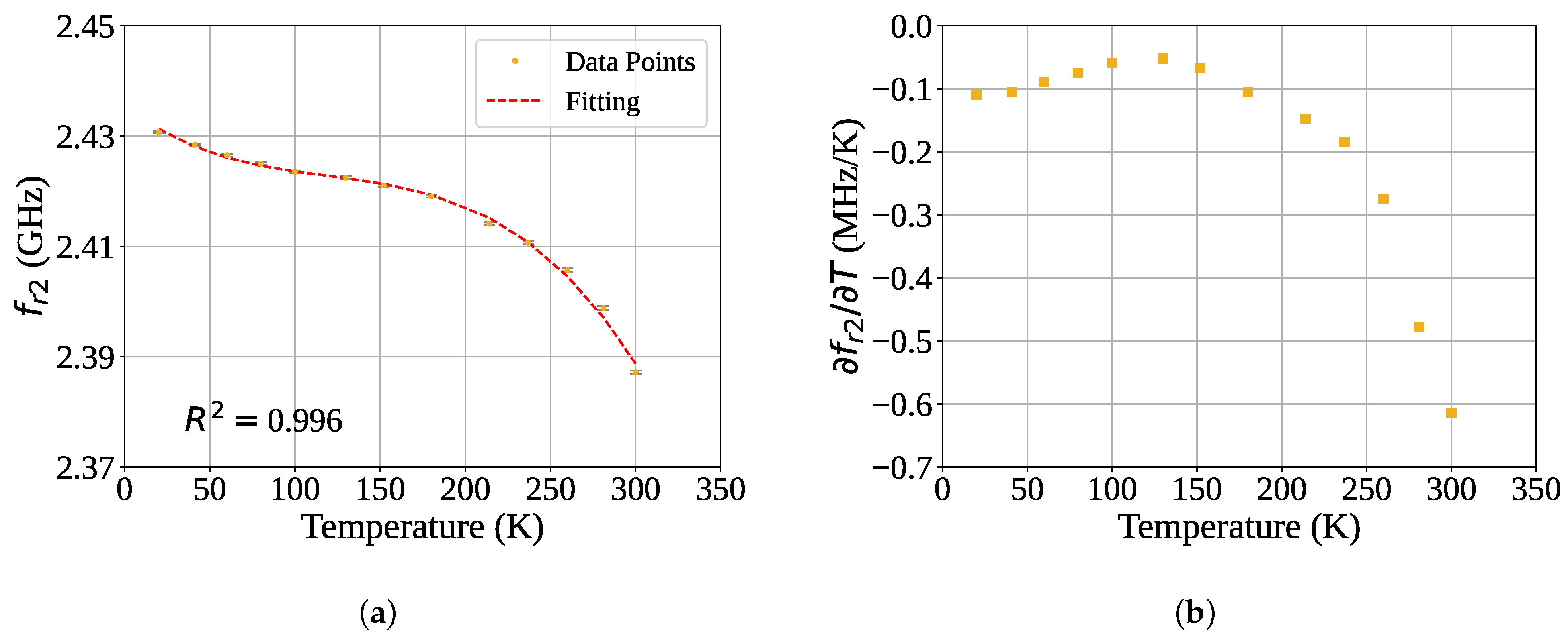
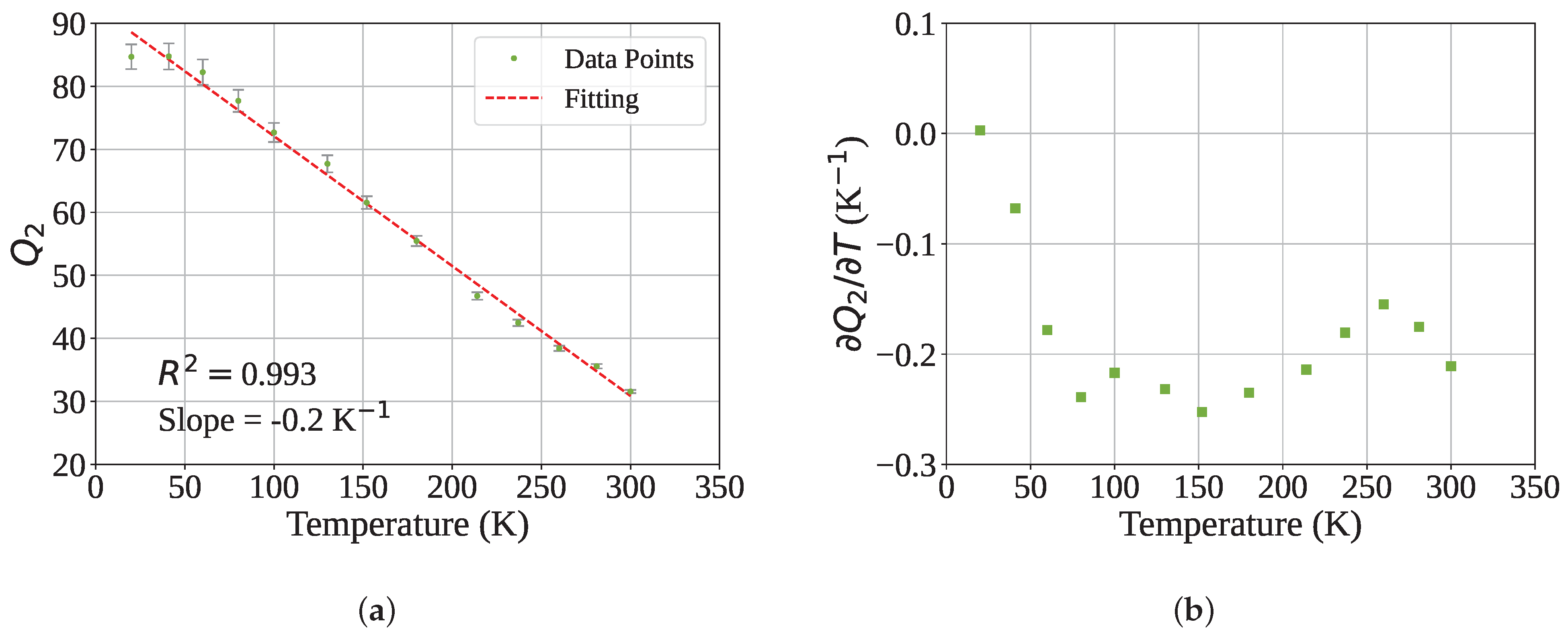
For its frequency- and temperature-dependent electrical characterization, the IDC was placed on a cryogenic thermal chuck inside of a stainless-steel chamber, as shown in Figure 7. The measurement setup included a cryogenic unit, a vacuum system, and an electrical characterization system. The cryogenic unit was used to cool the thermal chuck, acting as a two-stage closed-loop cryogenic refrigerator. The employed cryogenic system was a dual-stage CTI-Cryogenics recirculation helium system with a nominal temperature bottom limit of 10 K. To achieve the desired vacuum level, a Varian vacuum system consisting of a double-stage rotary pump and a turbomolecular pump was used. The vacuum level was monitored through thermocouple-based and cold cathode sensors. Figure 8 shows a schematic representation of the experimental setup. The electrical characterization system included an Agilent 3631A power supply connected to a power resistor that acted as an actuator for the chuck temperature control. A Keysight 34461 digital multimeter was used to measure the resistance of a cryogenic resistive extensometer, allowing the thermal chuck temperature to be evaluated. A VNA Agilent 8753ES was used to measure the IDC reflection coefficient. A frequency range from 100 MHz to 6 GHz was selected in this study, for a total of 1601 acquired points. Prior to the measurement process, a full two-port calibration procedure was performed on the VNA with a commercially available calibration kit using a short-open-load-through (SOLT) procedure. All components of the experimental setup were connected to a desktop computer through the IEEE 488.2 general-purpose interface bus (GPIB). This allowed the configuration of each instrument, as well as the chuck temperature, to be set using custom-made software.

3. Results

After the IDC had been placed inside the cryogenic chamber and a high vacuum level achieved, the reflection coefficient was measured from room temperature (i.e., 300 K) down to 20 K. The reflection coefficient was then converted into the corresponding admittance using the conversion formula [49]. This study primarily focuses on the first two resonances in the Y parameter, i.e., those at 932 MHz and 2.388 GHz. Both resonances are affected by temperature change, with a frequency shift towards lower frequencies observed as the temperature decreases. The peaks sharpness increases as well, corresponding to an increase in the Q-factor. In order to more accurately estimate the resonant parameters (i.e., the resonant frequency and Q-factor), a fitting procedure based on a Lorentzian function [50] was applied to the admittance parameter.
The first studied resonance occurred at 932 MHz (at 300 K). Figure 9 and Figure 10 show that the resonant frequency (i.e.,  f r 1 ) and Q-factor ( Q 1 ) are both temperature-dependent. As the temperature decreases, the resonant frequency shifts towards lower values while the Q-factor improves.
It should be noted that the error bars displayed in the figures correspond to the standard uncertainty of the measurements derived from both the Agilent 8753ES VNA and the fitting procedure. The measurement uncertainty of the VNA was determined using the VNA Uncertainty Calculator software from Keysight. As the temperature decreases, the sharpness of the peaks increases, which can negatively impact the accuracy of the fitting procedure. In fact, when the total number of acquired points is kept constant (at the maximum allowed by the VNA, i.e., 1601) and measurement conditions and VNA settings are both held constant as well, the peaks are inevitably described by a lower number of points due to a higher Q-factor. As a result, wider error bars are obtained.
For this resonance, the resonant frequency value does not exhibit a linear relationship with the temperature. Specifically, a linear trend is observed from 20 K to 100 K, followed by a constant range between 100 K and 250 K, then a sharp drop in resonant frequency for higher temperature values. This trend can be modeled with a fourth-order polynomial function, yielding an  R 2  value greater than 0.98. The sensitivity of  f r 1  with respect to temperature as determined by  f r 1 / T  is shown in Figure 9b. In contrast, the Q-factor shows a more linear trend with temperature ( R 2  approximately equal to 0.98), and its values and sensitivity with temperature (−0.2 K 1 ) are plotted in Figure 10b.
The second resonance, referred to as  f r 2 , is characterized by a monotonic trend from 2.435 GHz at 20 K to 2.388 GHz at 300 K. The relationship between  f r 2  and temperature can be accurately modeled with a third-order polynomial function with  R 2  > 0.99. The sensitivity of  f r 2  to temperature ranges from −0.1 MHz/K at 20 K to −0.58 MHz/K at 300 K. The resonant frequency and its sensitivity to temperature are illustrated in Figure 11. Figure 12 displays the Q-factor of the second resonance as a function of the temperature in the cryogenic chamber. The trend can be approximated as linear with good accuracy ( R 2  > 0.99), and exhibits a sensitivity of approximately −0.2 K 1 .
It can be observed that the resonances shift towards higher values as the temperature decreases towards cryogenic levels. This can be attributed to the thermal expansion effect of both the ink and the substrate, which results in a decrease in their size at lower temperatures, leading to a commensurate increase in the resonant frequency [51]. Another factor that may contribute to the resonant frequency shift is the temperature coefficient of the FR4 dielectric constant. The value of the dielectric constant decreases with lower temperatures [51], resulting in an increase in the resonant frequency. In fact, the IDC’s capacitance is proportional to the effective dielectric constant between the fingers. By considering the inductive contribution of the IDC as constant ( L e q ) with the temperature change, the equivalent capacitance ( C e q ) decreases with the FR4 dielectric constant, thereby increasing the resonant frequency; this can be expressed as  f r = 1 / ( 2 π L e q C e q )  [9].
Furthermore, an increase in the Q-factor is observed at cryogenic temperatures. The Q-factor is generally linked to Ohmic losses and dielectric losses [52]. Therefore, an increase in the Q-factor may be related to a rise in ink conductivity at cryogenic temperatures and/or a decrease in FR4 dielectric losses.

4. Conclusions

The study presented in this article aimed to investigate the frequency-dependent and temperature-dependent electrical properties of an inkjet-printed interdigitated capacitor. After proper characterization of the employed substrate material, a prototype was designed and fabricated by means of an inkjet printer by depositing a silver-based commercial ink on a commercial FR4 substrate. The goal of this research was to gain a better understanding of the behavior of inkjet-printed IDCs at cryogenic temperatures. This is relevant to a variety of different fields, and is especially applicable to sensing applications. In order to achieve this goal, the IDC was placed in a cryogenic chamber and the resonant parameters (i.e., resonant frequencies and Q-factors) were evaluated over a temperature range of 300 K to 20 K. For improved accuracy in the estimation of these parameters, a fitting procedure based on a Lorentzian function was applied. Our experimental results demonstrate that the resonant frequency of the IDC shifted towards higher values as the temperature decreased to cryogenic levels. Additionally, the Q-factor of the IDC increased at cryogenic temperatures. This behavior can be ascribed to changes in the physical properties of both the conductive ink and the substrate as the temperature changes (e.g., thermal expansion, conductivity, and permittivity).
This study investigated the characteristics of an inkjet-printed IDC fabricated on a low-cost FR4 substrate. In future research, it would be valuable to expand this investigation to include inkjet-printed devices using higher-performance substrates more typical for use in the microwave frequency range. This would allow for an assessment of the ink’s reliability on different substrates and at different frequency ranges. Additionally, it would be beneficial to conduct material characterization before and after cryogenic testing in order to identify any irreversible changes in the ink material. Finally, future investigations could explore the sensitivity of devices to additional external perturbations such as the presence of contaminants. A particular focus could be the impact of humidity on device performance, which could further enrich understanding of these devices’ behavior under different environmental conditions.

Author Contributions

Conceptualization, N.D. and E.S.; methodology, N.D.; software, G.G. and K.T; validation, G.C. and M.L.; formal analysis, G.G., A.A. and K.T.; investigation, G.G., A.A. and K.T.; data curation, G.C. and M.L.; writing—original draft preparation, G.G. and A.A.; writing—review and editing, G.G., A.A., M.L., G.C., K.T., E.S. and N.D.; supervision, E.S. and N.D. All authors have read and agreed to the published version of the manuscript.

Funding

This work has been partially funded by European Union (NextGeneration EU), through the MUR-PNRR project SAMOTHRACE (ECS00000022).

Institutional Review Board Statement

Not applicable.

Informed Consent Statement

Not applicable.

Data Availability Statement

Not applicable.

Conflicts of Interest

The authors declare no conflict of interest.

References

  1. Bailly, G.; Harrabi, A.; Rossignol, J.; Michel, M.; Stuerga, D.; Pribetich, P. Microstrip spiral resonator for microwave-based gas sensing. IEEE Sens. Lett. 2017, 1, 4500404. [Google Scholar] [CrossRef]
  2. Gugliandolo, G.; Aloisio, D.; Campobello, G.; Crupi, G.; Donato, N. On the design and characterisation of a microwave microstrip resonator for gas sensing applications. Acta Imeko 2021, 10, 54–61. [Google Scholar] [CrossRef]
  3. Gugliandolo, G.; Naishadham, K.; Crupi, G.; Donato, N. Design and characterization of a microwave transducer for gas sensing applications. Chemosensors 2022, 10, 127. [Google Scholar] [CrossRef]
  4. Alimenti, A.; Torokhtii, K.; Pompeo, N.; Silva, E. High precision and contactless dielectric loaded resonator for room temperature surface resistance measurements at microwave frequencies. In Proceedings of the 2022 IEEE International Instrumentation and Measurement Technology Conference (I2MTC), Ottawa, ON, Canada, 16–19 May 2022; pp. 1–6. [Google Scholar]
  5. Alimenti, A.; Torokhtii, K.; Vidal García, P.; Pompeo, N.; Silva, E. Design and Test of a New Dielectric-Loaded Resonator for the Accurate Characterization of Conductive and Dielectric Materials. Sensors 2023, 23, 518. [Google Scholar] [CrossRef] [PubMed]
  6. Alimenti, A.; Pittella, E.; Torokhtii, K.; Pompeo, N.; Piuzzi, E.; Silva, E. A dielectric loaded resonator for the measurement of the complex permittivity of dielectric substrates. IEEE Trans. Instrum. Meas. 2023, 72, 6001009. [Google Scholar] [CrossRef]
  7. Bao, X.; Ocket, I.; Crupi, G.; Schreurs, D.; Bao, J.; Kil, D.; Puers, B.; Nauwelaers, B. A planar one-port microwave microfluidic sensor for microliter liquids characterization. IEEE J. Electromagn. RF Microw. Med. Biol. 2018, 2, 10–17. [Google Scholar] [CrossRef]
  8. Bao, X.; Ocket, I.; Bao, J.; Liu, Z.; Puers, B.; Schreurs, D.M.P.; Nauwelaers, B. Modeling of coplanar interdigital capacitor for microwave microfluidic application. IEEE Trans. Microw. Theory Tech. 2019, 67, 2674–2683. [Google Scholar] [CrossRef]
  9. Crupi, G.; Bao, X.; Babarinde, O.J.; Schreurs, D.M.P.; Nauwelaers, B. Biosensor using a one-port interdigital capacitor: A resonance-based investigation of the permittivity sensitivity for microfluidic broadband bioelectronics applications. Electronics 2020, 9, 340. [Google Scholar] [CrossRef] [Green Version]
  10. Cuccaro, R.; Gavioso, R.; Benedetto, G.; Madonna Ripa, D.; Fernicola, V.; Guianvarc’h, C. Microwave determination of water mole fraction in humid gas mixtures. Int. J. Thermophys. 2012, 33, 1352–1362. [Google Scholar] [CrossRef]
  11. Corbellini, S.; Ramella, C.; Yu, L.; Pirola, M.; Fernicola, V. Whispering gallery mode thermometry. Sensors 2016, 16, 1814. [Google Scholar] [CrossRef] [Green Version]
  12. Gugliandolo, G.; Tabandeh, S.; Rosso, L.; Smorgon, D.; Fernicola, V. Whispering gallery mode resonators for precision temperature metrology applications. Sensors 2021, 21, 2844. [Google Scholar] [CrossRef] [PubMed]
  13. Gugliandolo, G.; Naishadham, K.; Crupi, G.; Campobello, G.; Donato, N. Microwave transducers for gas sensing: A challenging and promising new frontier. IEEE Instrum. Meas. Mag. 2022, 25, 42–51. [Google Scholar] [CrossRef]
  14. Gocen, C.; Palandoken, M. Machine Learning Assisted Novel Microwave Sensor Design for Dielectric Parameter Characterization of Water–Ethanol Mixture. IEEE Sens. J. 2021, 22, 2119–2127. [Google Scholar] [CrossRef]
  15. Carnerero-Cano, J.; Galindo-Romera, G.; Martínez-Martínez, J.J.; Herraiz-Martínez, F.J. A contactless dielectric constant sensing system based on a split-ring resonator-loaded monopole. IEEE Sens. J. 2018, 18, 4491–4502. [Google Scholar] [CrossRef]
  16. Javed, A.; Arif, A.; Zubair, M.; Mehmood, M.Q.; Riaz, K. A low-cost multiple complementary split-ring resonator-based microwave sensor for contactless dielectric characterization of liquids. IEEE Sens. J. 2020, 20, 11326–11334. [Google Scholar] [CrossRef]
  17. Aloisio, D.; Donato, N. Development of gas sensors on microstrip disk resonators. Procedia Eng. 2014, 87, 1083–1086. [Google Scholar] [CrossRef]
  18. Bogner, A.; Steiner, C.; Walter, S.; Kita, J.; Hagen, G.; Moos, R. Planar microstrip ring resonators for microwave-based gas sensing: Design aspects and initial transducers for humidity and ammonia sensing. Sensors 2017, 17, 2422. [Google Scholar] [CrossRef]
  19. Pittella, E.; Schiavoni, R.; Monti, G.; Masciullo, A.; Scarpetta, M.; Cataldo, A.; Piuzzi, E. Split Ring Resonator Network and Diffused Sensing Element Embedded in a Concrete Beam for Structural Health Monitoring. Sensors 2022, 22, 6398. [Google Scholar] [CrossRef]
  20. Tchafa, F.M.; Huang, H. Microstrip patch antenna for simultaneous strain and temperature sensing. Smart Mater. Struct. 2018, 27, 065019. [Google Scholar] [CrossRef]
  21. Bao, X.; Ocket, I.; Kil, D.; Bao, J.; Puers, R.; Nauwelaers, B. Liquid measurements at microliter volumes using 1-port coplanar interdigital capacitor. In Proceedings of the 2017 First IEEE MTT-S International Microwave Bio Conference (IMBIOC), Gothenburg, Sweden, 15–17 May 2017; pp. 1–4. [Google Scholar]
  22. Bao, X.; Ocket, I.; Bao, J.; Doijen, J.; Zheng, J.; Kil, D.; Liu, Z.; Puers, B.; Schreurs, D.; Nauwelaers, B. Broadband dielectric spectroscopy of cell cultures. IEEE Trans. Microw. Theory Tech. 2018, 66, 5750–5759. [Google Scholar] [CrossRef]
  23. Chehelcheraghi, M.; Franssens, V.; Ocket, I.; Nauwelaers, B. Real-Time kHz to GHz Monitoring of Incubated Yeast Cell Growth Using Interdigitated Capacitors. In Proceedings of the 2018 IEEE/MTT-S International Microwave Symposium-IMS, Philadelphia, PA, USA, 10–15 June 2018; pp. 1144–1147. [Google Scholar]
  24. Tesla, N. Electrical Condenser. U.S. Patent US567818A, 15 September 1896. [Google Scholar]
  25. Mamishev, A.V.; Sundara-Rajan, K.; Yang, F.; Du, Y.; Zahn, M. Interdigital sensors and transducers. Proc. IEEE 2004, 92, 808–845. [Google Scholar] [CrossRef] [Green Version]
  26. Love, A.E.H. Some electrostatic distributions in two dimensions. Proc. Lond. Math. Soc. 1924, 2, 337–369. [Google Scholar] [CrossRef]
  27. Bao, X.; Wang, Z.; Bao, J.; Gugliandolo, G.; Yuan, H.; Zhao, Z.; Li, J.; Donato, N.; Crupi, G.; Nauwelaers, B.; et al. Salt Content Detection Using a Microwave Sensor. In Proceedings of the 2022 IEEE International Workshop on Metrology for the Sea; Learning to Measure Sea Health Parameters (MetroSea), Milazzo, Italy, 3–5 October 2022; pp. 479–483. [Google Scholar]
  28. Bao, X.; Crupi, G.; Ocket, I.; Bao, J.; Ceyssens, F.; Kraft, M.; Nauwelaers, B.; Schreurs, D. Numerical modeling of two microwave sensors for biomedical applications. Int. J. Numer. Model. Electron. Netw. Devices Fields 2021, 34, e2810. [Google Scholar] [CrossRef]
  29. Wang, R.; Sun, H.; Jing, S.z.; Fan, Y. A Conformal Microwave Biosensor for Detecting Blood Viscosity. In Proceedings of the 2021 IEEE MTT-S International Microwave Workshop Series on Advanced Materials and Processes for RF and THz Applications (IMWS-AMP), Chongqing, China, 15–17 November 2021; pp. 25–27. [Google Scholar]
  30. Bailly, G.; Harrabi, A.; Rossignol, J.; Stuerga, D.; Pribetich, P. Microwave gas sensing with a microstrip interDigital capacitor: Detection of NH3 with TiO2 nanoparticles. Sens. Actuators B Chem. 2016, 236, 554–564. [Google Scholar] [CrossRef]
  31. Chen, W.; Stewart, K.; Mansour, R.; Penlidis, A. Novel undercoupled radio-frequency (RF) resonant sensor for gaseous ethanol and interferents detection. Sens. Actuators A Phys. 2015, 230, 63–73. [Google Scholar] [CrossRef]
  32. Yan, K.; Li, J.; Pan, L.; Shi, Y. Inkjet printing for flexible and wearable electronics. APL Mater. 2020, 8, 120705. [Google Scholar] [CrossRef]
  33. Gugliandolo, G.; Alimenti, A.; Torokhtii, K.; Pompeo, N.; Campobello, G.; Crupi, G.; Silva, E.; Donato, N. Design and test of an inkjet-printed microwave interdigital capacitor on flexible Kapton substrate. In Proceedings of the 2022 IMEKO TC4 Symposium, Brescia, Italy, 12–14 September 2022. [Google Scholar]
  34. Lee, H.; Shaker, G.; Naishadham, K.; Song, X.; McKinley, M.; Wagner, B.; Tentzeris, M. Carbon-nanotube loaded antenna-based ammonia gas sensor. IEEE Trans. Microw. Theory Tech. 2011, 59, 2665–2673. [Google Scholar] [CrossRef] [Green Version]
  35. Gugliandolo, G.; Vermiglio, G.; Cutroneo, G.; Campobello, G.; Crupi, G.; Donato, N. Inkjet-printed capacitive coupled ring resonators aimed at the characterization of cell cultures. In Proceedings of the 2022 IEEE International Symposium on Medical Measurements and Applications (MeMeA), Messina, Italy, 22–24 June 2022; pp. 1–5. [Google Scholar]
  36. Merilampi, S.L.; Virkki, J.; Ukkonen, L.; Sydänheimo, L. Testing the effects of temperature and humidity on printed passive UHF RFID tags on paper substrate. Int. J. Electron. 2014, 101, 711–730. [Google Scholar] [CrossRef]
  37. Voltera. Voltera Conductor 2 (1000388); Datasheet: Waterloo, ON, Canada, 2020. [Google Scholar]
  38. Koledintseva, M.Y.; Drewniak, J.L.; Hinaga, S. Effect of anisotropy on extracted dielectric properties of PCB laminate dielectrics. In Proceedings of the 2011 IEEE International Symposium on Electromagnetic Compatibility, Long Beach, CA, USA, 14–19 August 2011; pp. 514–517. [Google Scholar]
  39. Jackson, J.D. Classical Electrodynamics; American Association of Physics Teachers: Hoboken, NJ, USA, 1999. [Google Scholar]
  40. Chen, L.F.; Ong, C.; Neo, C.; Varadan, V.; Varadan, V.K. Microwave Electronics: Measurement and Materials Characterization; John Wiley & Sons: Hoboken, NJ, USA, 2004. [Google Scholar]
  41. Hsu, Y.W.; Shen, S.J.; Chen, C.A.; Qiu, S.H.; Chen, H.H. Broadband Measurement of Dielectric Constant on FR-4 PCB by Using Discontinuous Microstrip Lines. In Proceedings of the 2021 International Symposium on Antennas and Propagation (ISAP), Taipei, Taiwan, 19–22 October 2021; pp. 1–2. [Google Scholar]
  42. Alimenti, A.; Torokhtii, K.; Pompeo, N.; Piuzzi, E.; Silva, E. Characterisation of dielectric 3D-printing materials at microwave frequencies. Acta Imeko 2020, 9, 26–32. [Google Scholar] [CrossRef]
  43. Torokhtii, K.; Pompeo, N.; Silva, E.; Alimenti, A. Optimization of Q-factor and resonance frequency measurements in partially calibrated resonant systems. Meas. Sens. 2021, 18, 100314. [Google Scholar] [CrossRef]
  44. Djordjevic, A.R.; Biljié, R.M.; Likar-Smiljanic, V.D.; Sarkar, T.K. Wideband frequency-domain characterization of FR-4 and time-domain causality. IEEE Trans. Electromagn. Compat. 2001, 43, 662–667. [Google Scholar] [CrossRef]
  45. Joint Committee for Guides in Metrology. JCGM 101: Evaluation of Measurement Data—Supplement 1 to the Guide to the Expression of Uncertainty in Measurement—Propagation of Distributions Using a Monte Carlo Method; Technical Report; JCGM: Sèvres, France, 2008. [Google Scholar]
  46. Joint Committee for Guides in Metrology. JCGM 100: Evaluation of Measurement Data—Guide to the Expression of Uncertainty in Measurement; Technical Report; JCGM: Sèvres, France, 2008. [Google Scholar]
  47. Wang, C.; Ali, L.; Meng, F.Y.; Adhikari, K.K.; Zhou, Z.L.; Wei, Y.C.; Zou, D.Q.; Yu, H. High-accuracy complex permittivity characterization of solid materials using parallel interdigital capacitor-based planar microwave sensor. IEEE Sens. J. 2020, 21, 6083–6093. [Google Scholar] [CrossRef]
  48. Voltera. Questions about Our Products? 2022. Available online: https://www.voltera.io/faq (accessed on 4 May 2023).
  49. Pozar, D.M. Microwave Engineering; John Wiley & Sons: Hoboken, NJ, USA, 2011. [Google Scholar]
  50. Pompeo, N.; Torokhtii, K.; Leccese, F.; Scorza, A.; Sciuto, S.; Silva, E. Fitting strategy of resonance curves from microwave resonators with non-idealities. In Proceedings of the 2017 IEEE International Instrumentation and Measurement Technology Conference (I2MTC), Torino, Italy, 22–25 May 2017; pp. 1–6. [Google Scholar]
  51. Yan, D.; Yang, Y.; Hong, Y.; Liang, T.; Yao, Z.; Chen, X.; Xiong, J. Low-cost wireless temperature measurement: Design, manufacture, and testing of a PCB-based wireless passive temperature sensor. Sensors 2018, 18, 532. [Google Scholar] [CrossRef] [PubMed] [Green Version]
  52. Mekimah, B.; Messai, A.; Belhedri, A. Analysis of the effect of dielectric losses on the bandwidth of microstrip patch antenna in stacked geometry and modelling. SN Appl. Sci. 2020, 2, 767. [Google Scholar] [CrossRef] [Green Version]
Figure 1. Sketch of the microwave dielectric-loaded resonator used to measure the dielectric constant of the FR4 substrate. The lower and upper bases are made of brass, as is the sample holder. The dielectric crystal employed in the measurement is a sapphire cylinder of 5 mm height and 8 mm diameter. The TE011 mode is generated by means of coaxial cables that are ended with magnetic loops and operate at approximately 12.5 GHz. The dielectric sample is loaded beneath the upper base, and the resonator is closed by placing a 500 g weight on it. For further details, please refer to [42].
Instruments 07 00020 g001
Figure 2. Calibration curves  ε ( Δ f 0 / f 0 , a i r )  (black dots—left scale) and  η ( Δ f 0 / f 0 , a i r )  (red triangles—right scale), with  Δ f 0 = f 0 , s a m p l e f 0 , a i r , i.e., the difference between the resonance frequency  f 0 , s a m p l e  measured when the sample iswas loaded into the resonator and that of  f 0 , a i r  measured with the reference (air). The continuous curves were obtained by a second-order polynomial fit:  ε = 2.81 ( 3 ) × 10 4 ( Δ f 0 / f 0 , a i r ) 2 1.002 ( 2 ) × 10 3 Δ f 0 / f 0 , a i r + 1.002 ( 2 )  with  1 R 2 = 2.86 × 10 6  and  η = 72.95 ( 7 ) ( Δ f 0 / f 0 , a i r ) 2 2.1400 ( 3 ) Δ f 0 / f 0 , a i r + 1.9720 ( 4 ) × 10 3  with  1 R 2 = 1.38 × 10 8 . The uncertainty bars are within the dimensions of the symbols.
Instruments 07 00020 g002
Figure 3. A 2D sketch of the fabricated prototype. The IDC consists of a coplanar structure with nine fingers in a parallel configuration, and is printed on a 1.6-mm-thick FR4 substrate. All of the prototype’s nominal dimensions are reported in the figure.
Instruments 07 00020 g003
Figure 4. Photos of the IDC prototype: (a) Voltera V-One during the printing process and (b) fabricated prototype after curing and SMA connector soldering.
Instruments 07 00020 g004
Figure 5. Measurement (blue) and simulation (orange) of the admittance of the IDC in the frequency range from 100 MHz to 6 GHz, depicting (a) real and (b) imaginary parts. The measured Y is calculated from the IDC reflection coefficient acquired with the VNA in the same frequency range.
Instruments 07 00020 g005
Figure 6. Study of the IDC fabrication method’s reproducibility. Three samples were compared in terms of of the admittance parameter for both the real and imaginary parts, with the respective results shown in (a) and (b).
Instruments 07 00020 g006
Figure 7. Photo of the IDC prototype inside the stainless-steel chamber placed on the cryogenic thermal chuck. The power resistor and cryogenic resistive extensometer used for temperature actuation and control are depicted as well.
Instruments 07 00020 g007
Figure 8. Schematic representation of the cryogenic measurement system.
Instruments 07 00020 g008
Figure 9. Temperature dependence of the resonance at 932 MHz: (a) depicts the relationship between the resonant frequency and the temperature; the trend is modeled with a fourth-order polynomial function with a  R 2 = 0.984  (the red dashed line), while the sensitivity towards the temperature is shown in (b).
Instruments 07 00020 g009
Figure 10. Temperature dependence of the resonance at 932 MHz: (a) depicts the relationship between the Q-factor and the temperature; the trend can be considered linear with a good approximation ( R 2 > 0.98 ) (the red dashed line), while The sensitivity towards the temperature is shown in (b) and is about  0.2  K 1 .
Instruments 07 00020 g010
Figure 11. Temperature dependence of the resonance at 2.388 GHz: (a) depits the relationship between the resonant frequency and the temperature; the trend is modeled with a third-order polynomial function with a  R 2 = 0.996  (the red dashed line), while the sensitivity towards the temperature is shown in (b).
Instruments 07 00020 g011
Figure 12. Temperature dependence of the resonance at 2.388 GHz: (a) depicts the relationship between the Q-factor and the temperature; The trend can be considered linear with a good approximation ( R 2 > 0.98 ) (the red dashed line), while the sensitivity towards the temperature is shown in (b) and is about  0.2  K 1 .
Instruments 07 00020 g012
Table 1. “Conductor 2” ink properties [37].
PropertyValue
Sheet Resistance (50 µm film thickness)2.05 mΩ/sq
Resistivity (4-point-probe) 1.264 × 10 7 Ω·m
Typical cured film thickness50 µm
Density3.35 g/mL
Trace spread after print<20%
Recommended Nozzle ID150–225 µm
Typical Line Width150–100 µm
Typical Print height50–100 µm
Typical Feedrate300–500 mm/min
Typical Kick0.35 mm
Disclaimer/Publisher’s Note: The statements, opinions and data contained in all publications are solely those of the individual author(s) and contributor(s) and not of MDPI and/or the editor(s). MDPI and/or the editor(s) disclaim responsibility for any injury to people or property resulting from any ideas, methods, instructions or products referred to in the content.

