1. Introduction
Pixel detectors combining excellent spatial and temporal resolution with high detection efficiency and radiation tolerance are required for tracking detectors in future high-energy and high-rate particle collider experiments [
1,
2]. They also have wide-ranging applications in other fields, such as imaging Time-of-Flight Mass Spectroscopy and Fluorescence Life-Time Imaging Microscopy, medical applications such as proton therapy and sensors used in daily life, such as LIDAR in cars. Monolithic CMOS sensors, combining both a sensor and CMOS readout circuit in a single silicon wafer, are attractive candidates for providing such high-performance pixel detectors, due to their achievable large signal-to-noise ratios, advanced in-pixel signal processing circuitry and the availability of cost-efficient large-scale production.
A modified 180
CMOS imaging device with small, low-femtofarad collection electrodes on high-resistivity sensing layers has been used successfully to develop monolithic pixel sensors for various particle physics tracking detector projects [
3,
4,
5,
6]. The low capacitance helps to achieve a large signal-to-noise ratio, essential for high detection efficiency and sub-nanosecond timing. However, the small collection electrode design results in highly non-uniform electric fields in the sensor, causing the dependence of the charge collection time on where within the pixel the particle is incident, with typically much longer collection times if the charge is generated near the pixel edges. This represents a key limitation for both precise timing and radiation tolerance as slow charge collection increases the probability of the signal charge being captured by radiation-induced traps.
Within the ATTRACT FASTPIX project [
7], several sensor design modifications have been developed to overcome these limitations [
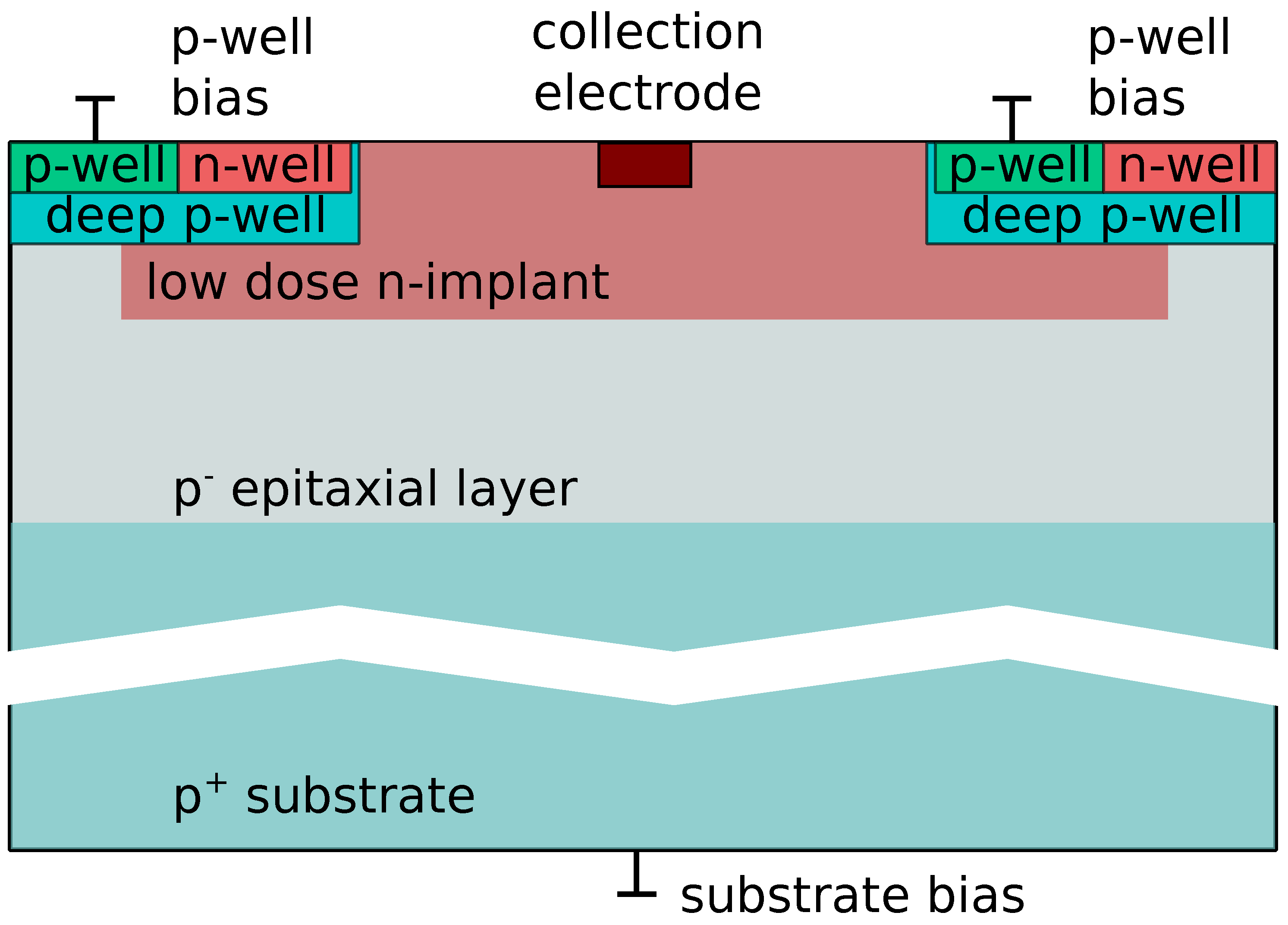
8]. Special implant structures have been designed that shape the electric field to uniformize the drift path within a pixel cell.
Figure 1 shows a schematic representation of an optimized sensor design. A hexagonal arrangement of the collection electrodes accelerates charge collection at the pixel edges, as the maximum distance within the pixel from the collection electrode is reduced. Moreover, the hexagonal pixel geometry is also favorable for timing and high detection efficiency, due to the reduced number of neighboring pixels, minimizing the charge sharing and therefore increasing the single-pixel signal-to-noise ratio.
Various combinations of the developed design modifications have been implemented in different variations of the ATTRACT FASTPIX monolithic timing demonstrator chip [
9].
2. Materials and Methods
2.1. The FASTPIX Chip
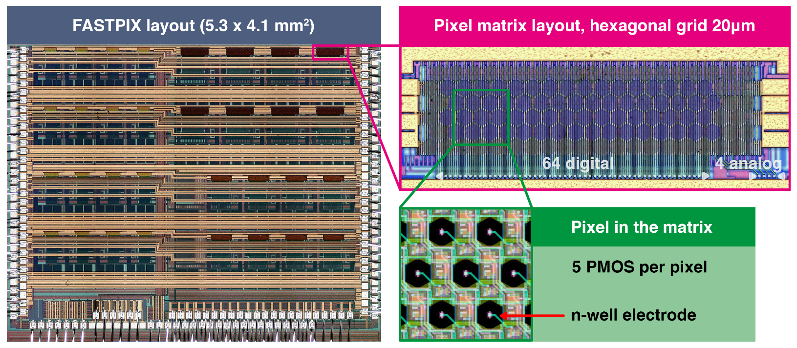
The FASTPIX demonstrator consists of 32 mini matrices with hexagonal pixels, split into 4 groups with a pixel pitch of
, 10
, 15
, and 20
. An overview of the matrix and pixel layout can be seen in
Figure 2. The 8 matrices in one group implement different sensor design parameters, such as the size of the collection electrode and geometry of the implant structures. Additionally, some of the wafers implement further modifications to the sensor design to accelerate charge collection. Each matrix has 64 pixels connected to the digital readout and 4 additional pixels with separate analog outputs.
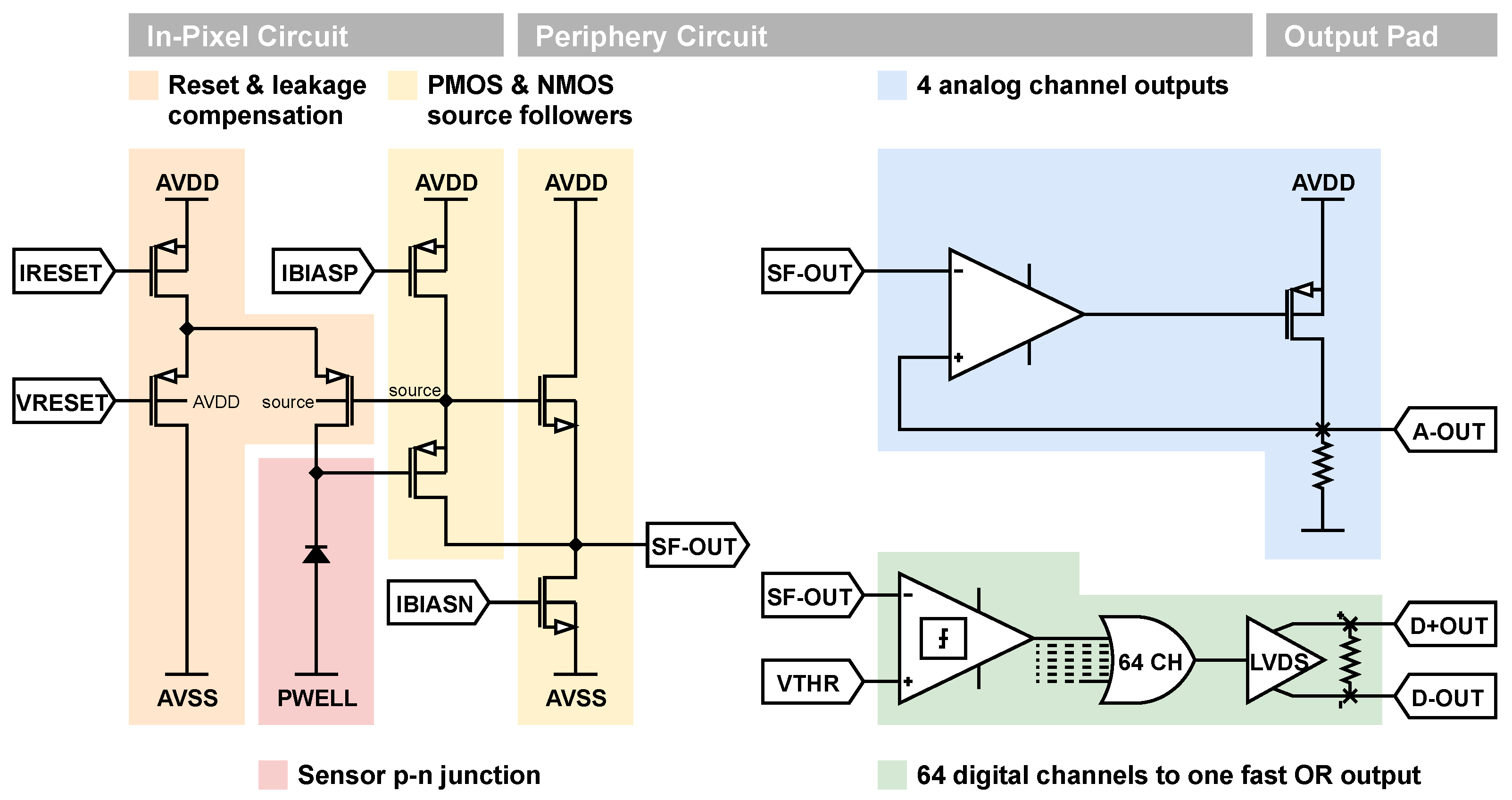
Figure 3 shows a schematic of the on-chip readout circuits for the analog and digital channels. Each pixel has a 2-stage amplifier with the first stage inside the pixel and the second stage in the periphery of the matrix. This is connected to an analog buffer for the analog channels or a discriminator with fast-OR logic and delay lines for the digital channels. The 68 active pixels in a matrix are surrounded by a ring of dummy pixels, similar to the active pixels but not connected to the readout.
2.2. Readout Architecture
The readout architecture of FASTPIX is asynchronous and processing of the discriminator signals is performed off-chip. The chip is equipped with three LVDS outputs. Each pixel discriminator creates a short pulse on the pixel output when crossing the threshold, leading to one pulse when exceeding the threshold and a second pulse when falling below the threshold again. Therefore, the Time-over-Threshold (ToT) is encoded in the time difference between these two pulses. The first LVDS output is a direct combination (OR) of all pixel outputs, giving the Time-of-Arrival (ToA) in the first pulse edge. Each pixel output is also fed into two delay lines running in opposite directions across the matrix, with a delay of typically 200 between pixels. With this, the pixel position is encoded in the time difference between two signal edges on the two delay lines. The other two LVDS outputs correspond to the output of these two delay lines.
2.3. Measurement Setup
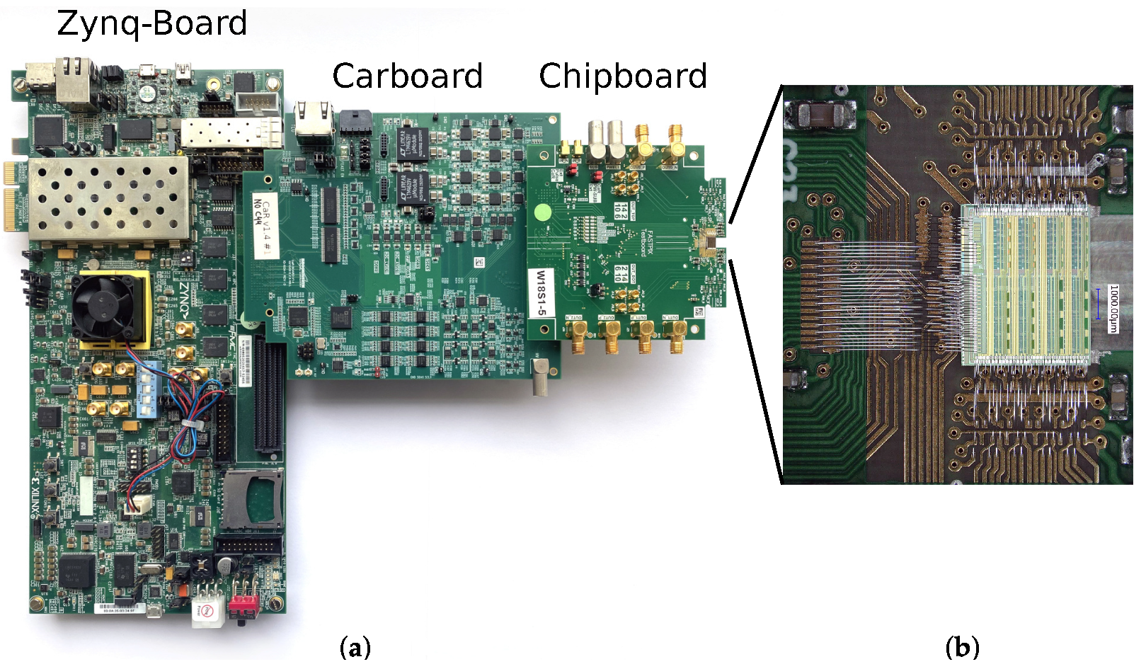
The FASTPIX chip is wire-bonded to a custom carrier board that connects to the Caribou readout system [
10] for power and control, as shown in
Figure 4. The Zynq board runs the Peary readout software and detector-specific firmware, while the Carboard provides power and bias voltages and currents, as well as the configuration of the chip. Readout of the digital or analog channels is performed with an Agilent DSO9254A oscilloscope with
analog bandwidth and a sampling rate of 10
S/
, which is also controlled by the Caribou system. This setup is used stand-alone for initial tests of the analog and digital readout, measurements with radioactive sources, and threshold calibration with external charge injection.
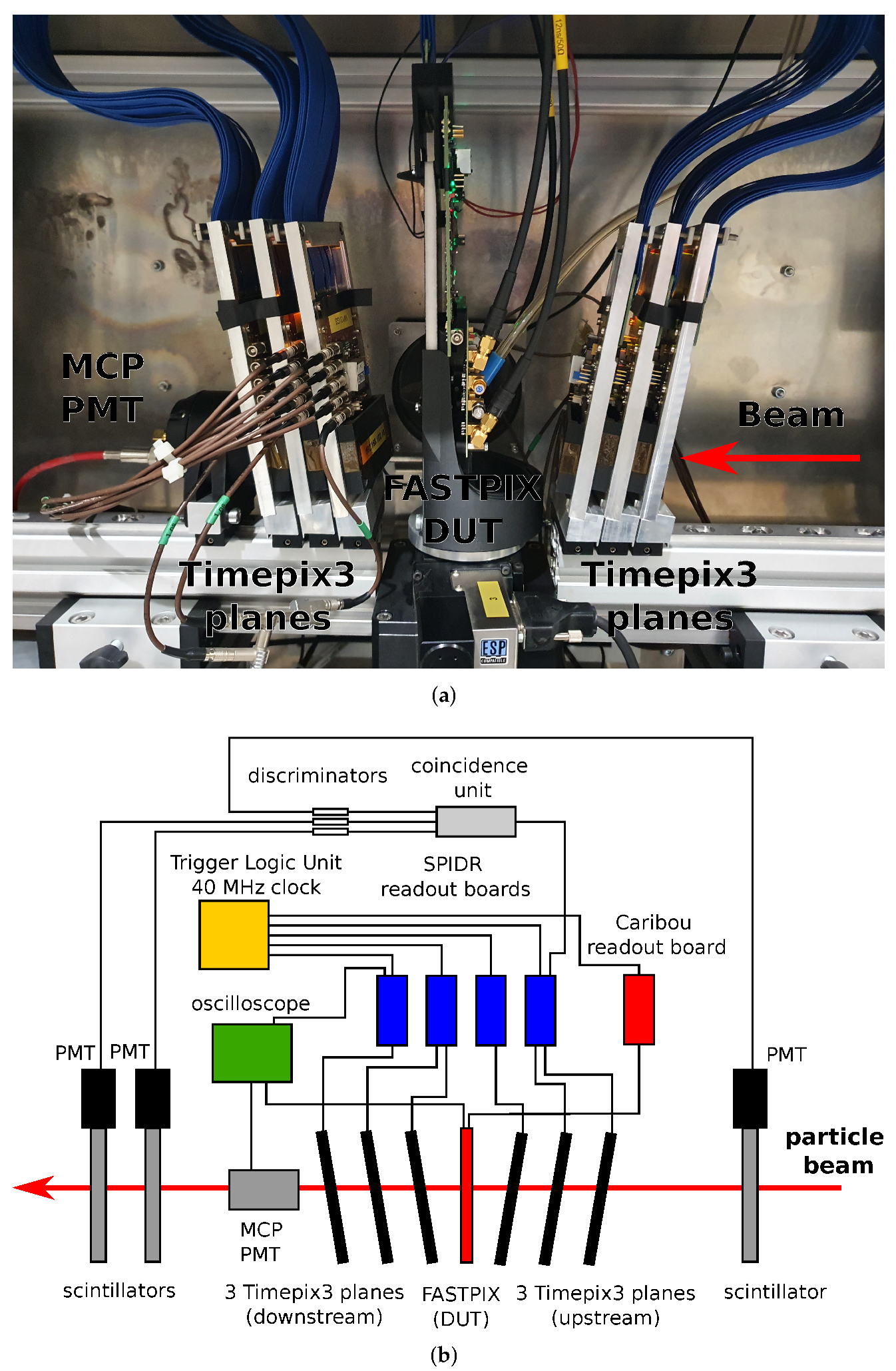
For measurements with beam particles, the setup is installed in the CLICdp Timepix3 beam telescope at the SPS North Area at CERN [
2]. A R3809U-50 Micro-Channel-Plate Photomultiplier Tube (MCP-PMT) by Hamamatsu is used as a timing reference [
11] and connected to the oscilloscope. A picture of the setup is shown in
Figure 5a, with a schematic view in
Figure 5b. The telescope consists of 6 Timepix3 assemblies mounted in a light-tight enclosure and connected to SPIDR readout boards [
12]. The FASTPIX is mounted in the center of the telescope on an x/y and rotation stage. The MCP-PMT is mounted behind the last downstream plane to minimize the amount of material in the telescope acceptance. One scintillator with a photomultiplier tube is installed before the upstream planes and two are installed behind the MCP-PMT and connected to a coincidence unit, which is connected to a TDC channel of the SPIDR readout.
Data acquisition of the oscilloscope is controlled by the Caribou system and integrated into the telescope DAQ. The oscilloscope trigger output is connected to a TDC of the SPIDR readout system to synchronize the data collection of both. The oscilloscope is triggered by the FASTPIX fast-OR LVDS signal and the pixel discriminator threshold is adjusted so that the currently read-out matrix does not exceed a noise rate of a few Hz. The FASTPIX is operated at bias at the substrate and p-wells. The MCP-PMT is operated at . The beam consists of Pions with a momentum of approximately 120 /c.
2.4. Analysis
Raw waveforms from to 350 around the trigger time are recorded, stored, and processed offline to extract pixel hits, ToT, and ToA information for FASTPIX and the MCP-PMT. For FASTPIX, the ToA is calculated from the first edge on the combined OR channel. Timing of the FASTPIX signals is determined by linear interpolation between samples, with a fixed threshold of 100 , which corresponds approximately to the 50% point of the LVDS outputs. The MCP-PMT operates as a time reference and the signals are required to exceed a 15 threshold and are processed with a constant fraction discriminator implemented in the software and set to 20% of the peak maximum.
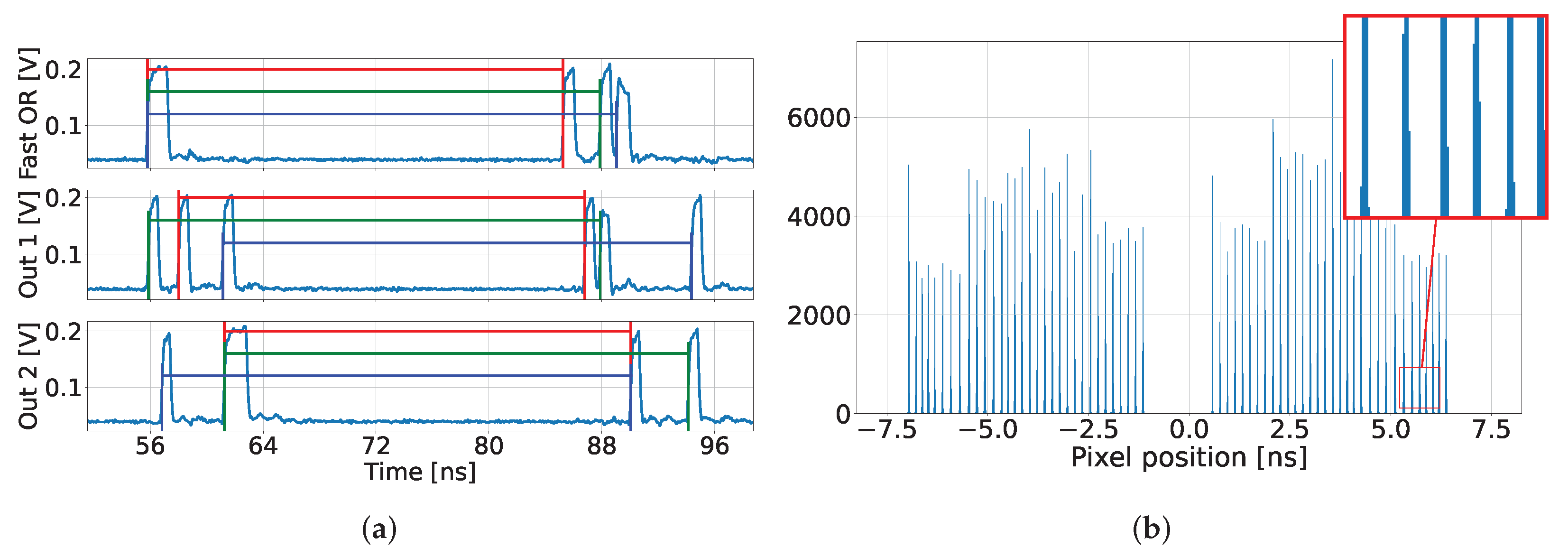
Figure 6a shows the recorded waveforms for an event with 3 pixel hits. Matching pairs of pulses with the same ToT across all 3 channels are connected with a line, and overlap between several pulses is visible.
Figure 6b shows the position of pixels along the delay line, calculated from single-pixel events. For decoding, the closest pixel on the delay line is determined and then translated into the physical position of the pixel. Pixels are connected to the delay lines in an interleaved pattern that reduces signal overlap from physically adjacent pixels in a cluster. Nevertheless, this scheme is still limited by overlap between signals from several pixels crossing the threshold simultaneously, as this introduces position reconstruction ambiguities. As 8 combinations of both rising and falling edges for both pairs of pulses can be used to calculate the pixel position, the correct position can still be identified in the event of some signal overlap, as long as the relative majority of combinations indicate the correct value. Pairs of pulses are matched by ToT across the 3 channels. The number of possible combinations also increases with the number of hits. To resolve some of the ambiguities, additional constraints can be used. For example, the pulses on the delay lines cannot arrive earlier than the corresponding pulse on the combined OR output, and the combined length of both delay lines is approximately constant for all pixels.
For each event, the pixel with the largest ToT is determined and the time residual of this pixel with respect to the time reference is calculated. To suppress MCP noise, each event is required to have exactly one peak from the MCP-PMT within the recorded window. Timewalk correction is performed by histogramming the time residual versus ToT on a pixel-by-pixel level and subtracting the mean of the corresponding histogram bin. To avoid bias from the timewalk correction, the data are split into two sets and the correction obtained from one set is applied to the other set.
2.5. Calibration
To determine the approximate operating threshold, a preliminary calibration with test pulses was performed. A charge signal can be injected externally into two digital pixels per matrix, and from this, the discriminator threshold and charge to ToT calibration are determined. An uncertainty of approximately 20% is expected, stemming from the uncertainty of the value of the injection capacitance.
The discriminator threshold and injected pulse amplitude are set by the Caribou system and the waveforms are recorded with an oscilloscope. The pulser circuit is switched with an external pulse generator. For each threshold, a range of injection pulses with different amplitudes is applied and the ratio
of the detected pulses and the total number of pulses is calculated. The threshold at the 50% point is determined with a fit to
where
is the pulser voltage,
is the pulser voltage at the 50% point, and
is the noise in the circuit, as shown in
Figure 7a.
is the complementary error function.
Figure 7b shows the measured threshold for the scanned range of the threshold setting for the pulseable pixels of a 10
and 20
pitch matrix.
Assuming a design value of 57 (10 pitch) and 54 (20 pitch) for the injection capacitance, the conversion factor from pulser voltage to injected charge is 356 e/ (10 pitch) and 337 e/ (20 pitch), which was used to calculate all threshold values stated here. The values are calculated from the mean of both pulseable pixels with the difference to the mean and an additional 20% on the injected charge as uncertainty. As only two pixels can be pulsed, pixel-to-pixel variations across the matrix cannot be determined.
The ToT calibration for each threshold is determined from the measured ToT over the range of injected pulses, which has a turn-on around the threshold and is linear for pulses well above the threshold. This is shown in
Figure 7c for one of the pixels. To estimate the charge corresponding to the peaks in the ToT spectra measured in the test beam, a linear fit is applied to the linear region and the associated value of
for a given ToT is determined. The values are again calculated from the mean of both pixels with the difference from the mean and an additional 20% as uncertainty.
3. Results
All measurements presented here were performed on a sample that was optimized for fast charge collection. The two investigated matrices have 10 and 20 pitch and are operated at a threshold DAC setting of and , which corresponds to a threshold of e and e, respectively. The difference from the mean is e (10 pitch) and e (20 pitch). The noise is e (10 pitch) and e (20 pitch).
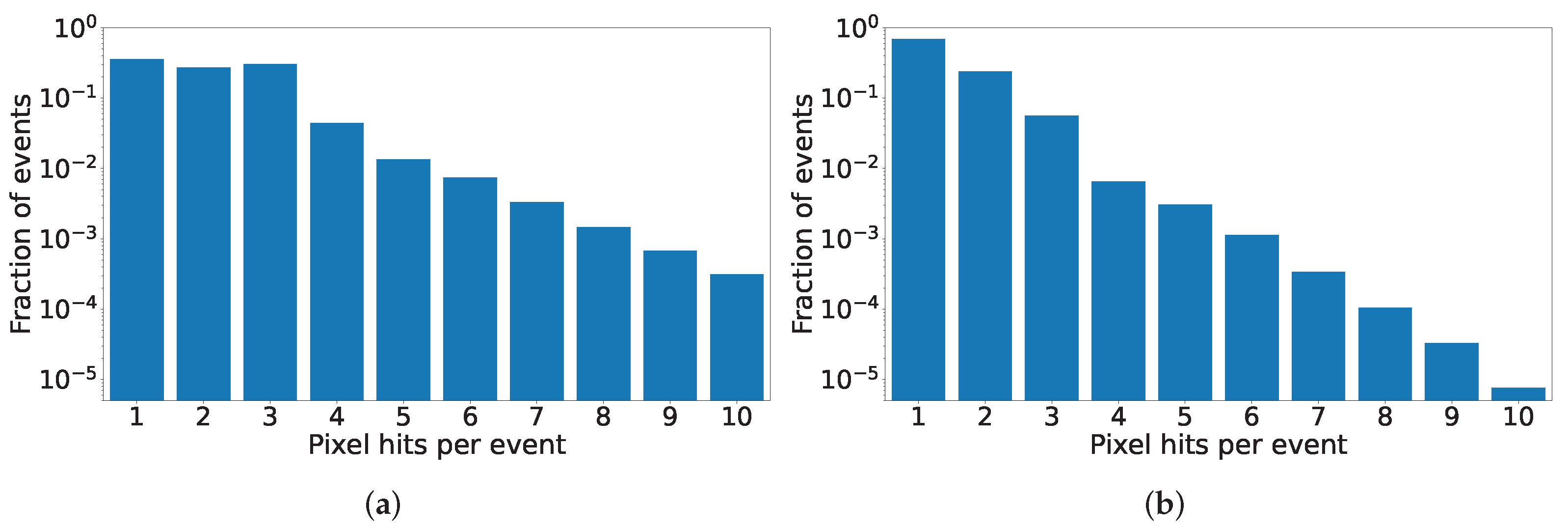
The number of pixel hits per event is shown in
Figure 8 for both matrices. A significant difference between the pitches is visible. The 20
pitch matrix has predominantly a single pixel hit per event, which is the case for 70% of events, and the fraction quickly drops off for more pixels. Moreover, 24% of events have two, and 5% have three pixel hits. The 10
pitch matrix has a similar fraction of single- (35%), two- (27%), and three- (31%) pixel events and then drops off. This shows that the smaller pitch leads to more charge sharing and indicates that the hexagonal layout limits this to mostly three or fewer pixels. Based on TCAD simulations for particles incident in the corner between pixels, an approximately 40% larger single-pixel charge signal is expected for the hexagonal design with 10
pixel pitch, compared to square pixels [
9].
A hitmap of the seed pixel, which is the pixel with the largest ToT in an event, is shown in
Figure 9 for the 20
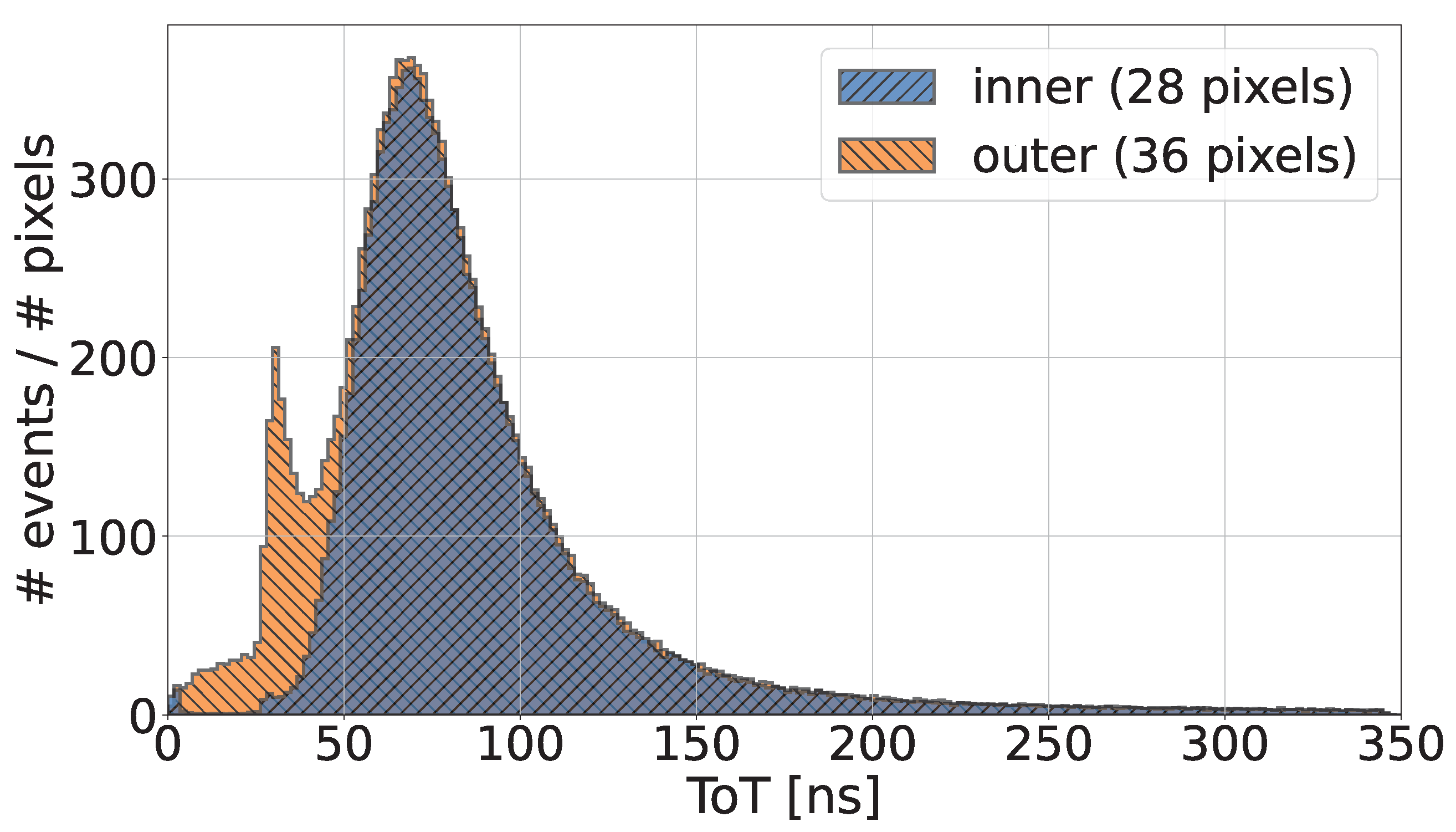
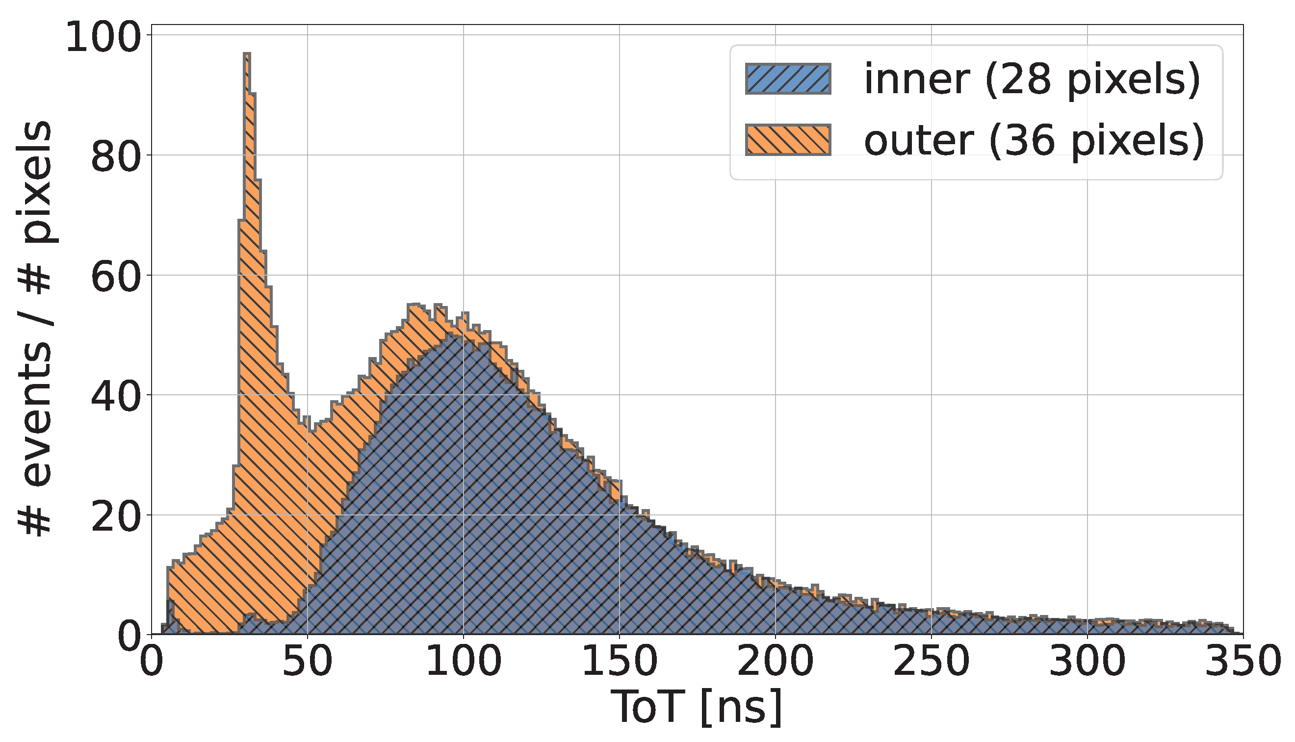
pitch matrix. A larger number of entries is visible for the pixels on the edge of the matrix, which also scales with the number of neighboring dummy pixels that surround the active matrix. The ToT spectrum of the seed pixels split into the inner and outer region can be seen in
Figure 10 for the 20
and in
Figure 11 for the 10
pitch matrix. A second peak in the spectrum is visible at a ToT of approximately 30
for the pixels on the border of the matrix. This suggests that the pixels on the border of the matrix receive an additional signal from hits outside the active area. The most probable ToT are 95
(10
pitch) and 67
(20
pitch), which correspond to a charge of
e and
e, respectively. The difference from the mean is
e for both.
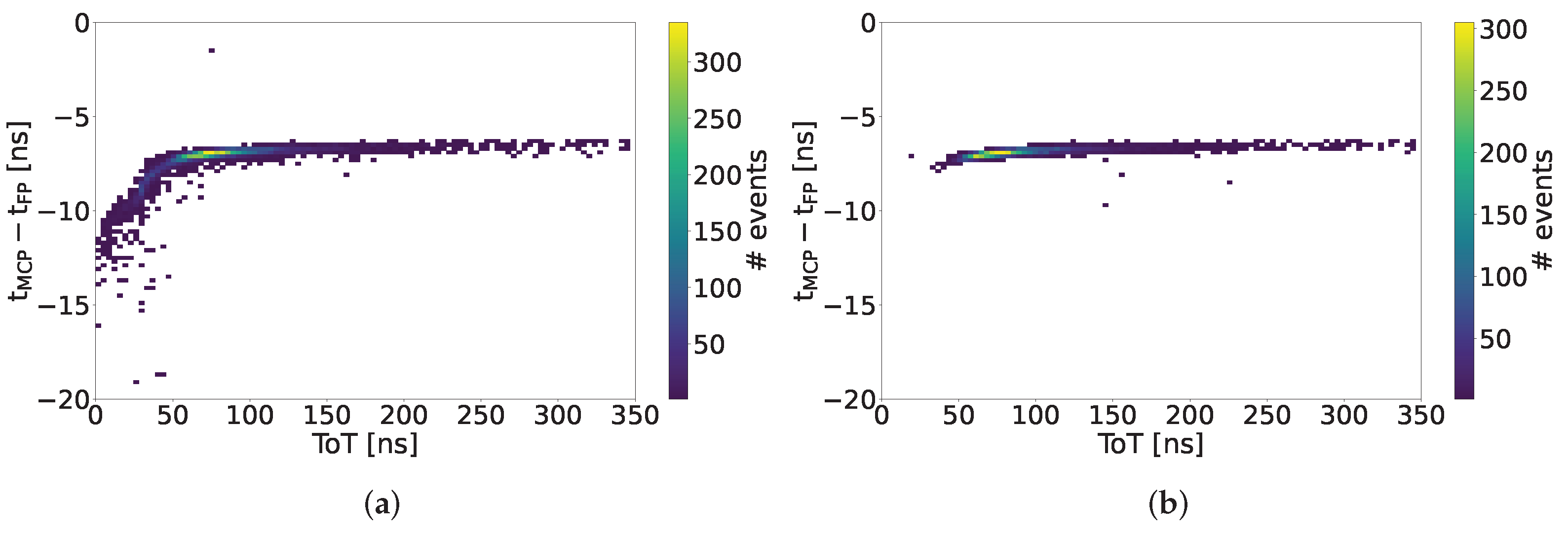
The timewalk plot in
Figure 12 shows the residuals depending on the ToT of the seed pixel for individual pixels. For the pixel on the matrix edge, additional entries in a broader band below 50
are visible, which result from charge sharing on the edge of the active matrix. To avoid edge effects on the border of the pixel matrix, the 36 pixels on the edge and the 28 pixels on the inside are investigated separately and only the timing performance of the inner region is investigated here, as shown in
Figure 13 before and after timewalk correction for the 20
pitch matrix.
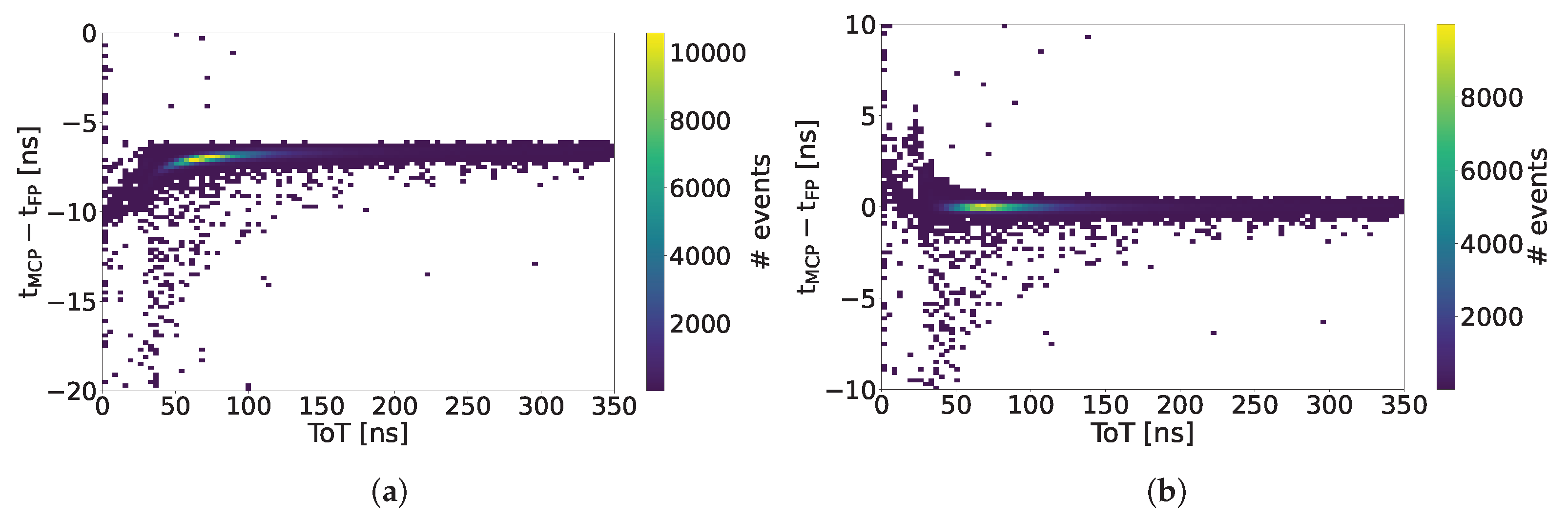
Figure 14 shows the residuals for 10
and 20
pitch after timewalk correction. Events with a ToT below 5
are discarded to reduce uncorrelated noise caused by noise coincidences of FASTPIX and the MCP-PMT. A time resolution of 135
and 122
is extracted from the Gaussian fit. The non-Gaussian tails for
indicate that the timewalk correction is unable to fully correct for timewalk effects. The reduced RMS of the central
interval (99.7% of data points) is
for the 10
and
for the 20
pitch matrix.
This still includes a contribution from the MCP-PMT and sampling. The time resolution of the MCP-PMT is expected to be below 10
[
11], resulting in a negligible contribution to the measured residuals. The contribution from sampling is estimated by measuring the jitter between the two lines of a FASTPIX LVDS output, which is below 5
RMS. The 10
pitch matrix has slightly worse timing performance than the 20
pitch matrix. While the smaller pitch leads to a shorter drift distance, it also leads to more charge sharing and a larger cluster size, resulting in a deteriorated time resolution for the seed pixel. The larger cluster size also leads to ambiguities for the pixel decoding. Misidentification of the pixel position could mix contributions from the edge of the matrix and the inner region and thereby further deteriorate the measured time resolution.


 ,
, 


