Article

Time Resolution of an Irradiated 3D Silicon Pixel Detector

1
Physics Institute, University of Zurich, 8057 Zurich, Switzerland
2
Jozef Stefan Institute, Jamova 39, SI-1000 Ljubjana, Slovenia
3
Centro Nacional de Microeletronica (IMB-CNM-CSIC), 08193 Barcelona, Spain
*
Author to whom correspondence should be addressed.
Instruments 2022, 6(1), 12; https://doi.org/10.3390/instruments6010012
Submission received: 14 November 2021 / Revised: 28 January 2022 / Accepted: 1 February 2022 / Published: 5 February 2022
(This article belongs to the Special Issue Timing Detectors)

Abstract

:
We report on the measurements of time resolution for double-sided 3D pixel sensors with a single cell of 50 μ m × 50 μ m and thickness of 285 μ m, fabricated at IMB-CNM and irradiated with reactor neutrons from 8 × 10 14 1MeV n e q /cm 2 to 1.0 × 10 16 1MeV n e q /cm 2 . The time resolution measurements were conducted using a radioactive source at a temperature of −20 and 20 °C in a bias voltage range of 50–250 V. The reference time was provided by a low gain avalanche detector produced by Hamamatsu. The results are compared to measurements conducted prior to irradiation where a temporal resolution of about 50 ps was measured. These are the first ever timing measurements on an irradiated 3D sensor and which serve as a basis for understanding their performance and to explore the possibility of performing 4D tracking in high radiation environments, such as the innermost tracking layers of future high energy physics experiments.

1. Introduction

The implementation of projects such as the HL-LHC [1] and FCC [2] is closely linked to the refinement of vertex detectors. Environmental conditions at the HL-LHC provide a unique challenge for detector design, where high spatial and temporal resolutions must be maintained in an extreme radiation environment. Among the various designs, 3D silicon pixel detectors are ideal candidates for the innermost layers of vertex trackers due to their inherent radiation hardness [3] and ability to provide time resolutions of the order of tens of picoseconds [4].
This technology, proposed by S.I. Parker and C. Kennedy in 1997 [5], is based on the use of vertical columns of electrodes that penetrate the bulk detector. Their particular geometry allows decoupling of the charge collection time and sensor thickness, making them intrinsically radiation tolerant due to the reduced power dissipation, smaller signal rise time and reduced trapping. We investigate whether the radiation hardness of such sensors also extends to their timing performance by measuring the time resolution before and after neutron irradiation up to 1.0 × 10 16 1MeV n e q /cm 2 ( n e q ). This paper is structured as follows. Section 2 describes the experimental setup and waveform analysis. Results are presented in Section 3 followed by conclusions in Section 4.

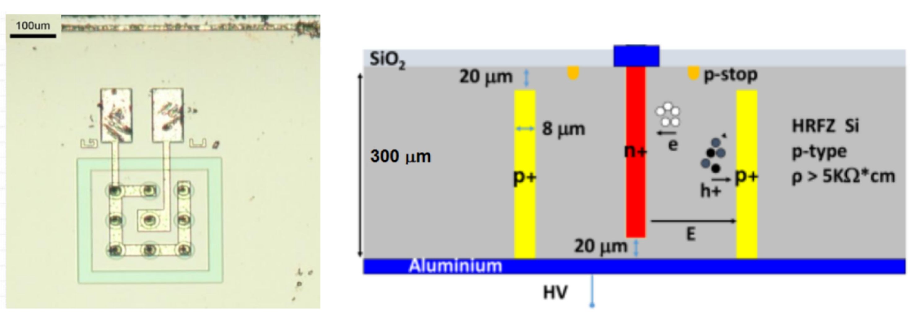
2. Materials and Methods

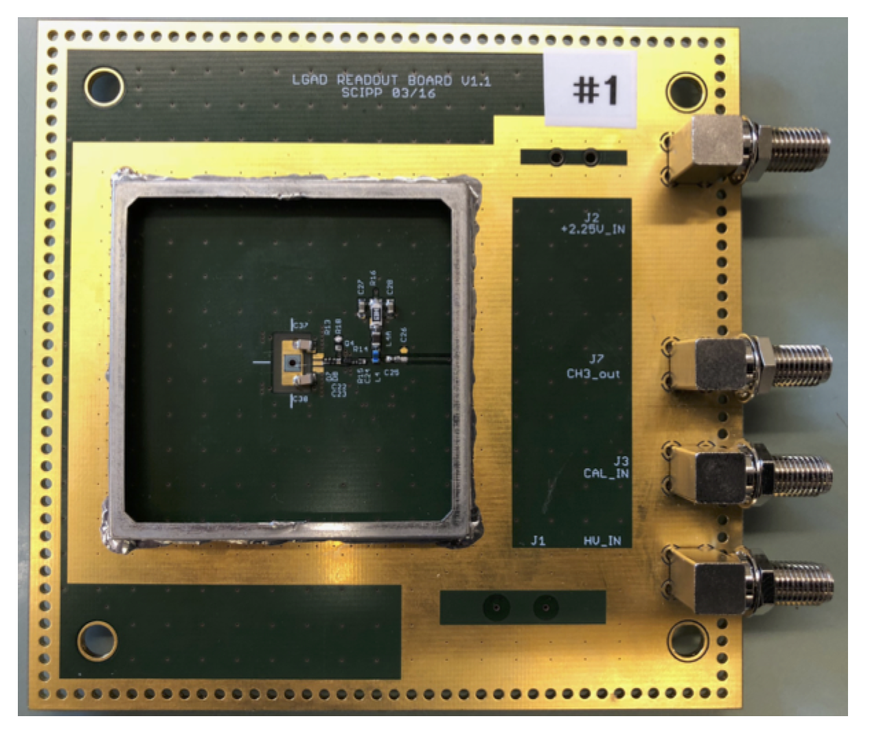
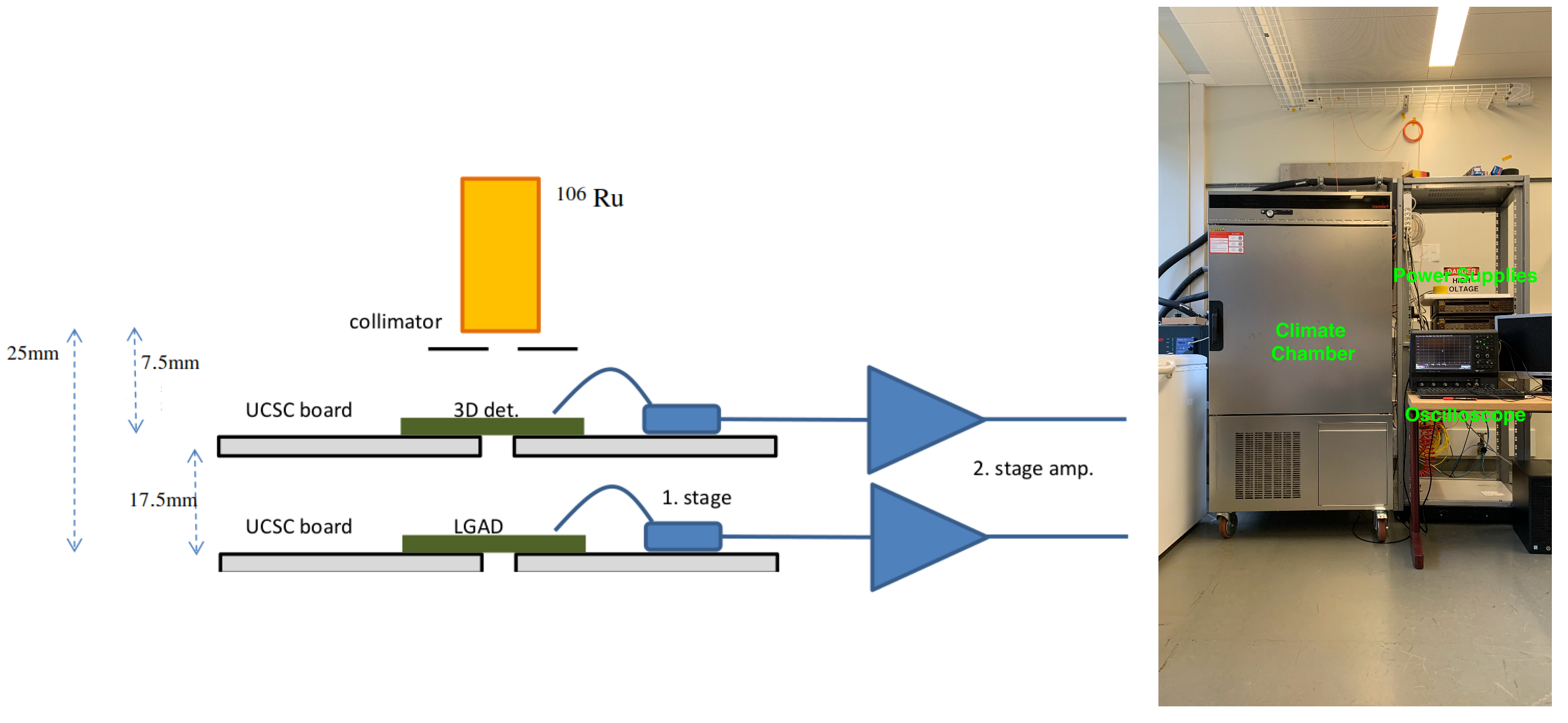
2.1. Experimental Setup

The 3D double-sided detectors used for the time resolution measurements described in this paper were produced at IMB-CNM [6] and their structure is shown in Figure 1. The central readout electrode n+ is surrounded by 8 p+ ohmic columns penetrating through a silicon substrate of 5 k Ω cm resistivity. It consists of 4 elementary cells with a size of (50 × 50) µm 2 and thickness of 285 µm. The diameter of the columns is 8–10 µm. The columns were etched from the top, while the four ohmic columns at each corner of the cell were etched from the bottom. Both column types penetrate some 20 µm short of the full thickness.
Sensors were wire bonded to a pre-amplifier board developed by the University of California Santa Cruz (UCSC) [7]. The board uses discrete components and contains several features which allow us to maintain a bandwidth of about 2 GHz and a relative low noise: by-pass capacitors located right next to the sensor, large ground planes, low impedance connections among layers, very short parallel wire-bonds to limit the inductance, and self-shielding packaging using lids which snap onto the boards on both sides. The inverting amplifier uses a high-speed SiGe transistor and it has a trans-impedance of about 470 Ω . A picture of a low gain avalanche detector (LGAD) bonded to a pre-amplifier board is shown in Figure 2.
Signals were generated with 3.5 MeV electrons from a 106 Ru source. After the pre-amplifier board, signals were sent to a Mini-Circuits ZX60-43+ second stage amplifier, with a gain of 14.35 dB and bandwidth of 4GHz [8] and then read out by a WaveRunner 8404M oscilloscope with a bandwidth of 4GHz. The sensor and pre-amplifier boards were placed in a Memmert CTC256 climate chamber in order to guarantee temperature stability and humidity control during the whole duration of the data taking. The temperature and humidity were measured by two sensors located on the interior walls of the climate chamber. The humidity level at −20 °C was measured to be about 50%. The time resolution was measured by considering signals in coincidence between the 3D sensor and a 50 μ m thick LGAD HPK50C [9] (1 mm diameter). Measurements were made for 3D bias voltages between 50 and 250 V in steps of 50 V and temperature of 20 and −20 °C, and a bias for the LGAD at 400V. A schematic and picture of the measuring set-up used is shown in Figure 3.
The 3D sensors were neutron irradiated with the TRIGA Mark II reactor at the Jozef Stefan Institute in Ljubljana. One sensor was tested before irradiation and underwent 3 different radiation exposures that brought the detector to a total fluence of 4.8 × 10 15 n e q , while an identical sensor was irradiated directly to 1.0 × 10 16   n e q . The fluences investigated are summarised in Table 1. After each irradiation, the sensor was annealed at 60 °C for 80 min, shipped to the Physics Institute at the University of Zurich, and tested.

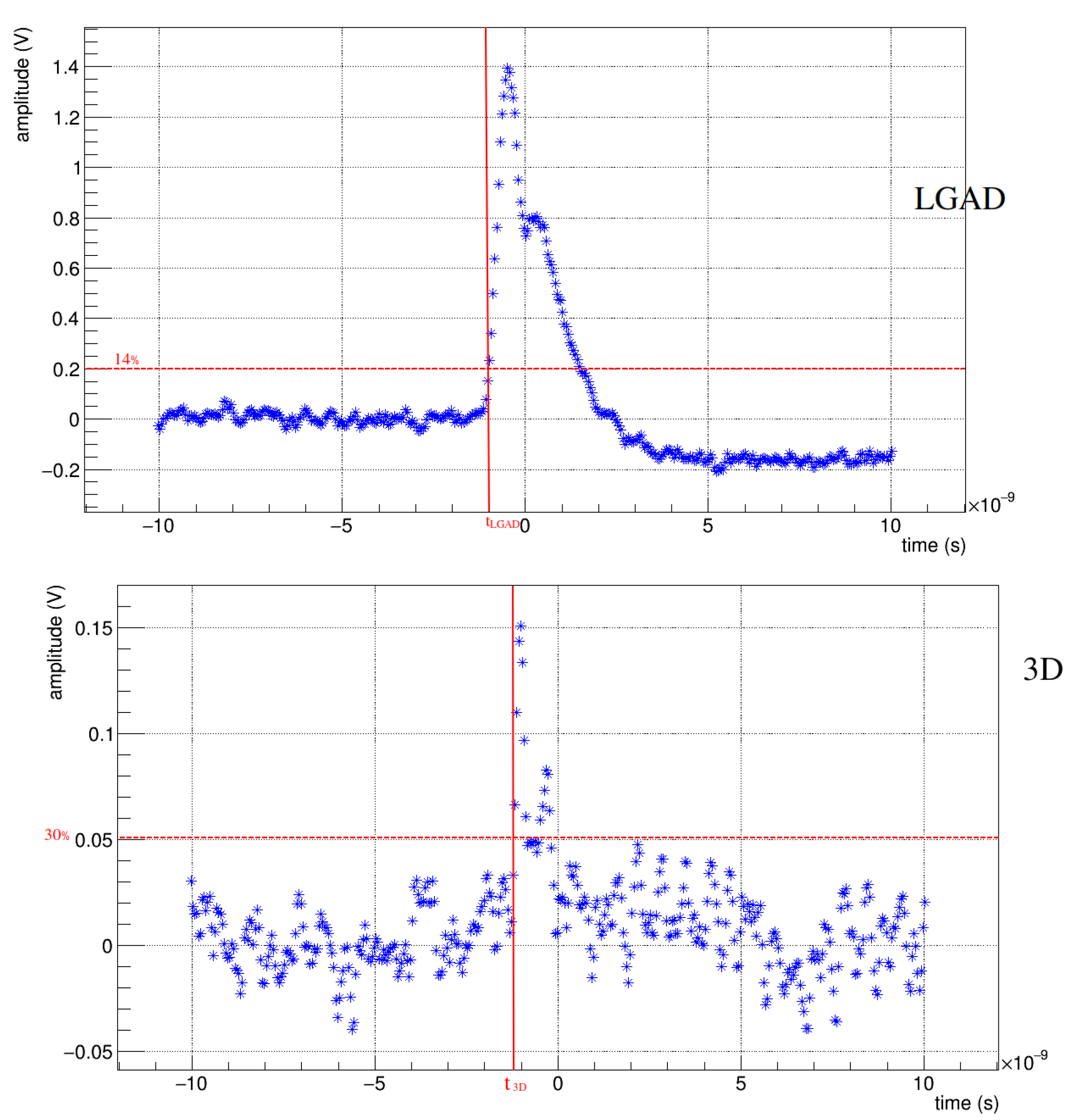
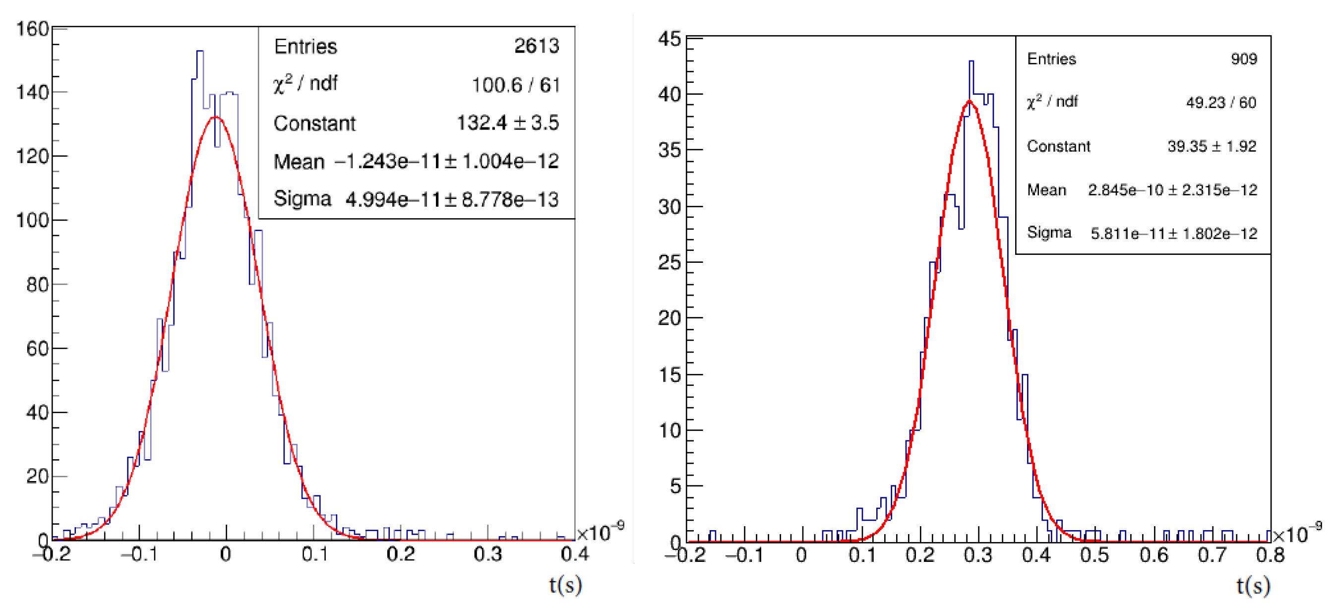
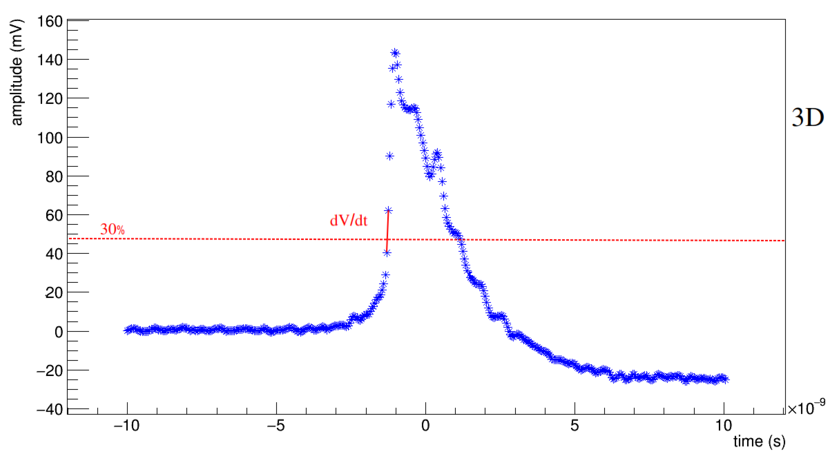
2.2. Waveform Analysis
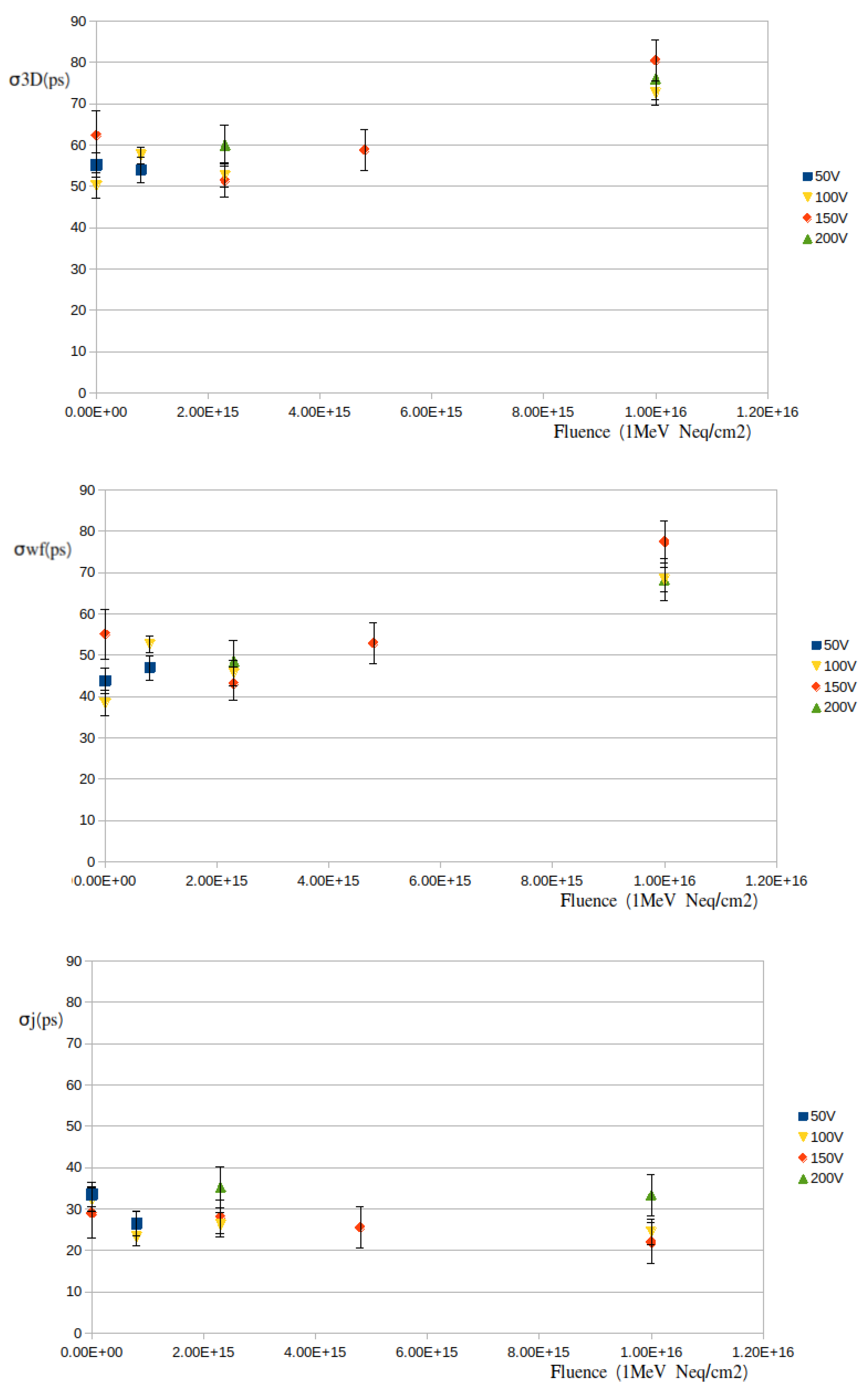
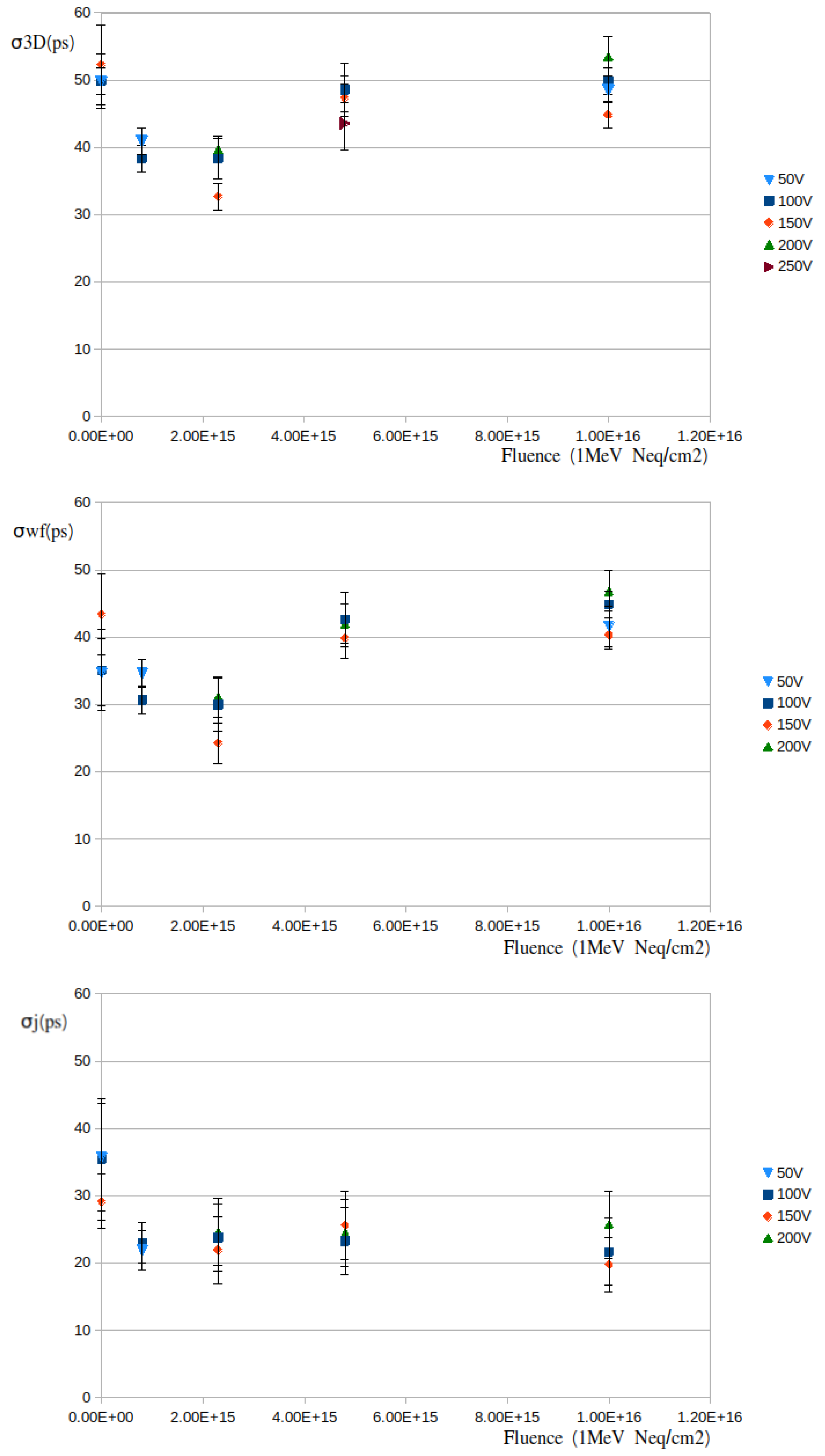
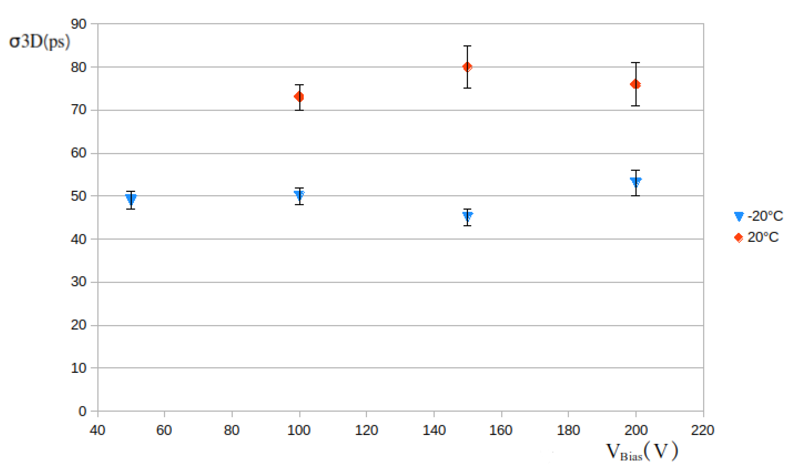
The time resolution was evaluated using a constant fraction discriminator (CFD) method, optimized to a threshold value of 14% for the LGAD and 30% for the 3D. The maximum of each signal was evaluated with a Gaussian fit on the peak. A polynomial fit on the rising edge of each of the two waveforms was used to determine the time when the signals crossed the discriminator threshold, denoted t L G A D and t 3 D for the LGAD and 3D, respectively. An example of the signal for both the LGAD and 3D are shown in Figure 4. The Gaussian fit to the time difference Δ t = t L G A D t 3 D between two the signals in coincidence is shown in Figure 5.
Before carrying out measurements on the 3D detector, the LGAD time resolution was measured at +20 °C and −20 °C. Two LGADs were wire-bonded to two different UCSC boards and measured in coincidence using the same setup as shown in Figure 3. The time resolution obtained from the fit, including a factor of 1 / 2 , is given in the Table 2.
Once the time resolution σ L G A D of a single LGAD is known, it is possible to obtain the 3D time resolution by σ 3 D 2 = σ t 2 σ L G A D 2 , where σ t is obtained from the fit on the right side of Figure 5.
Each step of the readout chain modifies the signal and can be broken into different terms affecting the time resolution approximated as
σ 3 D 2 σ T W 2 + σ j 2 + σ w f 2 + σ T D C 2 ,
where σ T W is the time-walk contribution, σ j is the electronic jitter, σ w f is the weight field contribution and σ T D C is the contribution from the TDC binning of the readout electronics. The time-walk contribution arises from signals of different amplitudes crossing the discriminator threshold at different times and includes also contributions from Landau fluctuations in charge generated in the sensor from a passing through particle. The electronic jitter arises from the interplay between the electronics and sensor and cause fluctuations of the signal baseline. The weight field term stems from variations in the collection times arising from non-uniformity of the electric field within the sensor. The time-walk term can be minimized by using a CFD method, while the term from the TDC binning is typically on the order of a few ps for a modern TDC. Both the time-walk and TDC terms are neglected from here on out, leaving only contributions from the jitter and weight field.
The ability to discern the individual contributions, σ w f and σ j , is fundamental to assess the feasibility of improving the intrinsic performance of this sensor by modifying its geometry. The jitter term σ j is evaluated as
σ j 2 = N d V d t | V T 2 ,
where N is the RMS of the noise determined from the baseline of the waveform in the region before signal peak, V is the signal and V T is the value of the signal at the CFD threshold. d V d t | V T is obtained by performing a linear fit around the threshold value of CFD on the graph obtained by averaging 1000 waveforms as shown in Figure 6. The value of σ w f is then derived by subtracting in quadrature the calculated value of σ j from the σ 3 D obtained previously.

3. Results

Figure 7 and Figure 8 (top) show the behaviour of the time resolution σ 3 D for 20 °C and −20 °C, respectively, at different bias voltage and as function of the fluence. The contribution of σ w f and σ j is evaluated using the procedure described in the previous paragraph and it is reported in Figure 7 and Figure 8 (center and bottom). The behaviour of the jitter contribution to the resolution is almost constant as fluence increases, while the σ w f contribution follows a different pattern. For the largest fluence at 20 °C the time resolution worsens by about 35%, while for measurements at −20 °C, the resolution is compatible with that of the not-irradiated sensor. The values before and after radiation exposures for a bias voltage value of 150 V are also reported in Table 3. At −20 °C the trend of σ w f decreases up to 2.3 × 10 15   n e q and increases for higher fluences. Measurements at different bias voltages at a fixed fluence and temperature are constant and within 1 or 2 standard deviations of each other, as seen in Figure 9.

4. Conclusions

We have presented the very first time resolution measurements of an irradiated 3D silicon pixel detector. The measurements were made for a voltage range between 50 V and 250 V. The sensor has been irradiated to different doses of radiation up to 1.0 × 10 16 n e q . A time resolution of less than 50 ps was achieved at 1.0 × 10 16 n e q at −20 °C and is compatible with the pre-irradiated value. This represents the most competitive time resolution for a highly irradiated silicon detector to date. It can also be seen that the variation in time resolution at different fluences, for 20 °C and −20 °C is dominated by σ w f .

Author Contributions

Conceptualization, G.P. and G.K.; methodology, G.P., G.K., M.M.; formal analysis, D.D.S.; investigation, D.D.S.; resources, N.S., G.K., G.P., C.B.; data curation, D.D.S.; writing—original draft preparation, D.D.S.; writing—review and editing, D.D.S.; supervision, C.B.; project administration, G.K.; All authors have read and agreed to the published version of the manuscript.

Funding

This work has been financed by the Swiss National Science Foundation, project code PZ00P2_179936, and the Spanish Ministry of Science and Innovation (MICIN) through the Particle Physics National Program RTI2018-094906-B-C22. All the manufacturing were performed at the IMB-CNM clean room facilities, member of the Spanish ICTS Network MICRONANOFABS partially supported by MICIN and FEDER funds.

Institutional Review Board Statement

Not applicable.

Informed Consent Statement

Not applicable.

Data Availability Statement

Not applicable.

Conflicts of Interest

The funders had no role in the design of the study; in the collection, analyses, or interpretation of data; in the writing of the manuscript, or in the decision to publish the results.

References

  1. Apollinari, G.; Brüning, O.; Nakamoto, T.; Rossi, L. Chapter 1: High Luminosity Large Hadron Collider HL-LHC; FERMILAB-PUB-15-699-TD. 2017. Available online: https://cds.cern.ch/record/2120673 (accessed on 13 November 2021). [CrossRef]
  2. Abada, A.; Abbrescia, M.; AbdusSalam, S.S.; Abdyukhanov, I.; Fernandez, J.A.; Abramov, A.; Aburaia, M.; Acar, A.O.; Adzic, P.R.; Agrawal, P.; et al. FCC-hh: The Hadron Collider. Eur. Phys. J. Spec. Top. 2019, 228, 755–1107. [Google Scholar] [CrossRef]
  3. Lange, J.; Giannini, G.; Grinstein, S.; Manna, M.; Pellegrini, G.; Quirion, D.; Terzo, S.; Vázquez Furelos, D. Radiation hardness of small-pitch 3D pixel sensors up to a fluence of 3 ×10¹⁶ neq/cm2. J. Instrum. 2018, 13, P09009. [Google Scholar] [CrossRef] [Green Version]
  4. Kramberger, G.; Cindro, V.; Flores, D.; Hidalgo, S.; Hiti, B.; Manna, M.; Mandić, I.; Mikuž, M.; Quirion, D.; Pellegrini, G.; et al. Timing performance of small cell 3D silicon detectors. Nucl. Instrum. Methods Phys. Res. Sect. A 2019, 934, 26–32. [Google Scholar] [CrossRef] [Green Version]
  5. Parkera, S.I.; Kenneya, C.J.; Segal, J. 3D—A proposed new architecture for solid-state radiation detectors. Nucl. Instrum. Methods Phys. Res. Sect. A 1997, 395, 328–343. [Google Scholar] [CrossRef]
  6. Pellegrini, G.; Balbuena, J.P.; Bassignana, D.; Cabruja, E.; Fleta, C.; Guardiola, C.; Lozano, M.; Quirion, D.; Ullán, M. 3D double sided detector fabrication at IMB-CNM. Nucl. Instrum. Methods Phys. Res. Sect. A 2013, 699, 27–30. [Google Scholar] [CrossRef]
  7. Cartiglia, N.; Staiano, A.; Sola, V.; Arcidiacono, R.; Cirio, R.; Cenna, F.; Ferrero, M.; Monaco, V.; Mulargia, R.; Obertino, M.; et al. Beam test results of a 16 ps timing system based on ultra-fast silicon detectors. Nucl. Instrum. Methods Phys. Res. Sect. A 2017, 850, 83–88. [Google Scholar] [CrossRef]
  8. Available online: https://www.minicircuits.com/ (accessed on 13 November 2021).
  9. Galloway, Z.; Fadeyev, V.; Freeman, P.; Gkougkousis, E.; Gee, C.; Gruey, B.; Labitan, C.A.; Luce, Z.; McKinney-Martinez, F.; Sadrozinski, H.F.-W.; et al. Properties of HPK UFSD after neutron irradiation up to 6e15n/cm2. Nucl. Instrum. Methods Phys. Res. Sect. A 2019, 940, 19–29. [Google Scholar] [CrossRef] [Green Version]
Figure 1. Schematic view from top of a single cell structure (left). Cross section of a single cell structure (right) [4].
Instruments 06 00012 g001
Figure 2. Picture of a sensor bonded to a UCSC pre-amplifier board.
Instruments 06 00012 g002
Figure 3. Experimental setup used for measurements of the time resolution.
Instruments 06 00012 g003
Figure 4. An example of the waveform from an LGAD (B) and 3D detector (B). The red lines indicate the CFD threshold value and corresponding timestamp on the signal.
Instruments 06 00012 g004
Figure 5. Distribution of Δ t in the configuration with two LGADs at −20 °C (left). Distribution of Δ t in the configuration 3D-LGAD (right) with the 3D detector irradiated at a fluence of 1.0 × 10 16 n e q , at a temperature of −20 °C for a bias voltage of 150 V.
Instruments 06 00012 g005
Figure 6. Example of 1000 averaged waveforms for the 3D detector.
Instruments 06 00012 g006
Figure 7. Time resolution vs. fluence for different bias voltages at 20 °C. Top: σ 3 D , middle: σ w f , and bottom: σ j .
Instruments 06 00012 g007
Figure 8. Time resolution vs. fluence for different bias voltages at −20 °C. Top: σ 3 D , middle: σ w f , and bottom: σ j .
Instruments 06 00012 g008
Figure 9. Time resolution σ 3 D vs. bias voltage at 20 and −20 °C for 1.0 × 10 16 n e q .
Instruments 06 00012 g009
Table 1. Radiation exposures.
8 × 10 14   n e q
2.3 × 10 15   n e q
4.8 × 10 15   n e q
1.0 × 10 16   n e q
Table 2. Time difference between two LGADs in coincidence.
Temp. (°C)CFD (%) σ LGAD (ps)
+201438.0 ± 0.7
−201435.3 ± 0.9
Table 3. Time resolution measurements at 150 V for different radiation doses.
+20 °C σ 3 D (ps) σ w f (ps) σ j (ps)
not irradiated62 ± 655 ± 629 ± 5
2.3 × 10 15 n e q 51 ± 443 ± 328 ± 5
4.8 × 10 15 n e q 59 ± 553 ± 326 ± 5
1.0 × 10 16 n e q 80 ± 568 ± 222 ± 4
−20 °C σ 3 D (ps) σ w f (ps) σ j (ps)
not irradiated52 ± 643 ± 629 ± 4
2.3 × 10 15   n e q 33 ± 224 ± 322 ± 5
4.8 × 10 15   n e q 47 ± 240 ± 326 ± 5
1.0 × 10 16   n e q 45 ± 240 ± 220 ± 4
Publisher’s Note: MDPI stays neutral with regard to jurisdictional claims in published maps and institutional affiliations.

