Article

Design and Optimization of Potentially Low-Cost and Efficient MXene/InP Schottky Barrier Solar Cells via Numerical Modeling

by
Mohammad Saleh N Alnassar
Department of Electrical Engineering, College of Engineering, Qassim University, Buraydah 51452, Saudi Arabia
Condens. Matter 2024, 9(1), 17; https://doi.org/10.3390/condmat9010017
Submission received: 16 January 2024 / Revised: 22 February 2024 / Accepted: 29 February 2024 / Published: 3 March 2024

Abstract

:
This paper uses numerical modeling to describe the design and comprehensive analysis of cost-effective MXene/n-InP Schottky barrier solar cells. The proposed design utilizes Ti3C2Tx thin film, a 2D solution-processible MXene material, as a Schottky transparent conductive electrode (TCE). The simulation results suggest that these devices can achieve power conversion efficiencies (PCEs) exceeding 20% in metal–semiconductor (MS) and metal–interlayer–semiconductor (MIS) structures. Combining the proposed structures with low-cost InP growth methods can reduce the gap between InP and other terrestrial market technologies. This is useful for specific applications that require lightweight and radiation-hard solar photovoltaics.

1. Introduction

Renewable energy sources, such as biomass, geothermal, wind, and solar are available for sustainable use if effectively managed. Among these sources, solar energy stands out as the most promising and rapidly expanding alternative for commercial and domestic power needs [1]. The renewable energy industry has witnessed remarkable growth due to technological advancements in materials science and solar photovoltaic cell processing techniques. The absorber (or base layer), which is responsible for light absorption, is a key factor in the high efficiency of solar cells [2].
Due to its direct bandgap of ~1.34 eV, which is well-matched to the solar spectrum, indium phosphide (InP) is a promising absorber material for high-efficiency solar photovoltaic cells. This is in addition to its superior radiation hardness [3], as well as its absorption coefficient, which is considerably larger than that of its close competitor (GaAs) over the energy range of 1.30–2.7 eV [4], making it particularly attractive for settings with high radiation levels, such as space, nuclear, and high-altitude environments. Despite these desirable features, InP is still not competitive in the terrestrial solar cell market [5]. Some of the reasons why this is the case are the high processing costs and the epitaxial growth requirements [5,6]. The champion InP solar cell is a metal organic chemical vapor deposited (MOCVD) n+/p/p+ homojunction structure that requires multiple doping-controlled epitaxial growth steps in addition to growing lattice-matched passivation window layers, both of which are examples of costly materials and processing [7]. The power conversion efficiency (PCE) of the InP champion cell, at ~24.2%, lags behind that of the GaAs cell, which is ~29.1% [8], and falls short of the Shockley–Queisser limit of ~33.7% for homojunction InP [9]. These figures suggest that there is room for improving these cells’ efficiency.
Research efforts to reduce the cost of InP solar cells have been ongoing since the late 1970s. Over the years, researchers have explored alternative structures to the costly p+/n or n+/p InP homojunction. These alternatives include n-ITO/p-InP [10,11,12,13], n-CdS/p-InP [14,15,16], and other heterojunctions that utilize carrier selective contacts such as TiO2 [17] and ZnO [18,19]. Additionally, InP-based Schottky junctions that consist of metal–semiconductor (MS) and metal–intermediate layer–semiconductor (MIS) structures have also been investigated [20,21,22]. In these early experimental investigations, conventional metals such as Au or Pt (on n-type InP) and Al or Sb (on p-type InP) were used to fabricate MS and MIS Schottky barrier solar cells and reported PCEs of ≤7% measured under different conditions (AM 2 and AM 0). The intermediate layer commonly used in these studies is an ultrathin insulating material (InP anodic oxide) grown by anodizing the prepared surface of the InP substrate. Nowadays, intermediate layers beyond insulating oxides, known as Hole Transport-Electron Blocking Layer (HT-EBL) materials for n-type semiconductors and Electron Transport-Hole Blocking Layer (ET-HBL) materials for p-type semiconductors are investigated for use in MIS solar cells [23]. The InP solar cell has achieved PCEs of ~19.3% with fewer fabrication steps [5,17], thanks to combined research efforts for cost reduction. One of the most significant advancements is eliminating the need for MOCVD and epitaxial growth techniques [5].
Schottky barrier solar cells are the simplest to fabricate, requiring low thermal budgets, making them ideal for exploring novel materials and designs [24] and potentially low-cost for terrestrial applications. Such cells are commonly fabricated by depositing a thin metal layer with a high work function onto the top surface of an n-type semiconductor substrate with moderate doping [25]. As with any semiconductor device, low-resistance ohmic contacts are required and, therefore, formed on the back surface of the substrate (absorber layer) in these cells by depositing metal layers having work functions lower than that of an n-type semiconductor [26]. However, the front metal (semimetal) layer must be chemically and mechanically stable, optically transparent, and exhibit low resistance for efficient Schottky solar cells [27]. Finding a Schottky contact material for InP that satisfies these conflicting requirements is challenging; hence, fabricating efficient InP-based Schottky barrier solar cells remains elusive.
Two-dimensional materials, such as graphene and TMDs, are highly conductive and optically transparent and have lately been used to design innovative optoelectronic devices, including solar cells [28,29]. Two-dimensional materials and semiconductors forming Schottky junctions are promising for low-cost solar cells. The 2D materials act as transparent conductive electrodes (TCEs) and active layers to effectively collect and separate photoexcited carriers from semiconductors in these cells. The use of a novel class of 2D materials, known as MXenes (transition metal carbides, nitrides, and carbonitrides) [30], in solar photovoltaics has piqued the interest of experts since the first study in 2018 [31] due to their favorable attributes, including metallic electrical conductivity, high carrier mobility, excellent transparency, and exceptional mechanical properties. Recent experimental evidence showed that a prominent member of the MXene family, named titanium carbide MXene (Ti3C2Tx), where Tx represents different surface functional groups, such as −F, −O, and −OH, forms a high-quality large Schottky-barrier-height junction with n-Si and n-GaAs, resulting in an initial (unoptimized) PCEs of 5% and 9.69% [32,33], respectively.
Motivated particularly by the promising results obtained from MXene/n-GaAs solar cells [33], this paper presents, for the first time, the numerical modeling and optoelectronic simulation results obtained from MXene/n-InP Schottky solar cells designed using PC1D version 5.9 simulation software [34]. Benefiting from the tunable work function and high transparency of solution-processible Ti3C2Tx thin film, this study investigates the potential use of this material as a Schottky TCE in combination with InP, a notable absorber material. The performance of these types of solar cells is systematically assessed by examining the critical structure and material parameters that influence both basic MS and more efficient MIS structures. Simulation parameters and models are initially calibrated using experimental data from the literature to ensure accuracy. This study provides valuable insights into the potential of low-cost MXene/InP solar cells, guiding future research.

2. Numerical Modeling and Simulation Methodology

The drift-diffusion transport equations for semiconductors serve as the basis for modeling solar cell physics. Specifically, the following system of five equations is considered:
J n = μ n n E F n
J p = μ p p E F p
n t =   ·   J n q + G L U n  
p t =   ·   J p q + G L U p
2 ϕ = ρ ε  
where q is the elementary charge. In this system, Equations (1) and (2) relate the electron and hole current densities (Jn and Jp) to the mobilities (μn and μp), densities (n and p), and quasi-Fermi levels (EFn and EFp) of electrons and holes. Equations (3) and (4), referred to as the continuity equations, explain how electrons and holes move into and out of a semiconductor device by accounting for their flow into and out of a given region in the device, as well as the creation and annihilation processes within it (known as generation and recombination processes) using the electron–hole pairs generation rate (GL) and electron and hole recombination rates (Un and Up). These equations are used to monitor the distribution and changes in the concentration of charge carriers over time. The final equation in the system, Equation (5), is Poisson’s equation, which relates the electrostatic potential ϕ to the charge density per unit volume ρ and dielectric constant ε of a given region within the simulated device. Using the finite element method, PC1D solves this nonlinear partial differential equation system in one dimension with the appropriate boundary conditions derived from the device’s realistic operational conditions. This approach has proven robust and accurate for various devices [27,35,36,37,38], including InP-based solar cells [39,40,41]. The simulations presented here are based on Boltzmann charge carrier statistics, recommended when implementing the default bandgap narrowing model in the simulations:
n = N C   e E C E F n k T  
p = N V   e E F p E V k T  
Here, NC and NV are the effective density of states in the conduction and valence bands, EC is the conduction band lower edge, Ev is the valence band upper edge, k is Boltzmann’s constant, and T is the temperature. The parameters in the default bandgap narrowing model (PC1D5.9 BGN) were carefully calibrated to closely match the empirical model by Bugajski et al. [42] for n-type InP, as depicted in Figure 1, which gives good agreement with values measured experimentally. The default parameters of the low-field doping and temperature-dependent mobility model in PC1D are also changed to agree with the updated, more accurate model for InP by Sotoodeh et al. [43]. Table 1 shows the new parameters. Radiative (band-to-band) and Auger recombination processes are accounted for by adjusting the relevant parameters, in addition to doping and temperature-dependent Shockley–Read–Hall (SRH) recombination within the cell’s bulk and at its surfaces. According to R.K. Ahrenkiel in [44], the data on minority carrier lifetimes and surface recombination velocities (SRVs) in n-InP show significant variation. The lifetimes can range from as low as 0.01 μs to 3.5 μs, while the SRVs can range from 200 cm s−1 to 5 × 103 cm s−1. These large variations depend on the growth method, material surface quality, and the measurement method used.
The schematic diagrams of MS and MIS structures designed in PC1D are shown in Figure 2. The two structures differ only by the presence of an ultrathin semi-insulating SI-InP layer. It can be realized using various methods, such as ion implantation of Fe, reaching resistivities >107 Ω·cm, corresponding to a carrier concentration of ~1.2 × 108 cm−3 [45]. If SI-InP retains desirable InP properties and is lattice-matched with the n-type absorber in the MIS structure, the MIS solar cells are expected to outperform the MS cells due to dark current reduction [20,21].
Schottky junctions are modeled in PC1D with a nonzero ‘surface barrier’ at the MS interface, causing band bending consistent with the semiconductor type. The ‘surface barrier’ value in this case is equivalent to the built-in potential barrier (qVbi), as seen by the semiconductor electrons near the metal-to-n-semiconductor interface. Negative (positive) surface barrier values simulate upward (downward) band bending. The Schottky barrier height (Φb) is related to the built-in potential barrier qVbi by the equation Φb = qVbi + kT/q ln(NC/ND), where ND is the donor doping concentration of the semiconductor. The Schottky barrier height is also related to the metal’s (Ti3C2Tx MXene) work function ΦM by the equation Φb = ΦM − χInP, where χInP is the electron affinity of the semiconductor (n-InP), assuming a metal/n-InP semiconductor junction obeying the Schottky–Mott model [46].
Modeling the MIS structure in PC1D is quite different from modeling the MS one, as including the intermediate layer gives rise to an additional potential barrier to the assumed ‘surface barrier’ value described above. The carrier concentration significantly drops when crossing from the n-InP region to the ultrathin SI-InP region, creating this additional potential barrier, given by kT/q ln(ND/1.2 × 108). Therefore, qVbi* can be defined as the overall built-in potential barrier, as seen by semiconductor electrons in the MIS structure due to both contributions. It is related to the ‘surface barrier’ value entered as a model parameter in PC1D by the equation qVbi* = qVbi + kT/q ln(ND/1.2 × 108), accounting for the band bending observed across both regions. It is important to note that in the MIS structure, the metal is in direct contact with the SI-InP. Thus, Φb = qVbi + kT/q ln(NC/1.2 × 108).
A Ti3C2Tx colloidal solution with a concentration of 0.01 mg mL−1 offered the optimum TCE thin film properties (work function of ~5.5 eV, transmittance ~90%, and series resistance of ~10 Ω) [33]. Consequently, these values will serve as inputs in the initial simulation of the designed MXene/InP solar cell, which has an active area of 1 cm2. Table 2 lists the simulation parameters used in this work. The Ti3C2Tx TCE thin film slightly improved the reflectance of GaAs upon introduction, and a reflectance of less than 16% was reported after the double-layer antireflection coating (DLARC) deposition of ZnS/MgF2 [33]. The reflectance of InP is slightly less than that of GaAs (32.7% for InP and 35.9% for GaAs), as calculated by the OPAL 2 optical simulator [47] using refractive index data from Palik [48] and Aspenes et al. [49], respectively. Thus, this study assumes an average conservative reflectance value of 15% for the initial simulations. For completeness, the proposed solar cells were simulated under terrestrial AM 1.5G and space AM 0 spectra to assess if they yield dissimilar optimization outcomes.

3. Results and Discussions

To confirm the formation of a Schottky junction between the n-InP absorber layer and the Ti3C2Tx TCE, initial simulations were conducted under equilibrium conditions for the solar cell structures depicted in Figure 2, using the parameters listed in Table 2. The simulation results were used to assess the energy band diagrams and junction electrostatics. For the MS structure, an assumption was made that Φm = 5.50 eV and ND = 1 × 1015 cm−3. Based on this, the value of qVbi was determined to be ~0.956 eV, which was used as the front surface barrier value in the initial simulation (Table 2). The simulation shows that a Schottky barrier height Φb of ~1.12 eV is formed, as illustrated by the energy band diagram for the MS structure in Figure 3a. It should be noted that this figure depicts the region of the n-InP layer where band bending takes place, which is within the first two micrometers from the MS junction.
Figure 3b shows the effect of adding the 1 nm thick SI-InP layer (the MIS structure) on the energy band diagram, with an inset displaying the events occurring in the first five nanometers from the MI junction. As expected, based on the MIS discussion in Section 2, the resulting overall built-in potential barrier qVbi* of ~1.368 eV is composed of the front surface barrier used in simulating the MS structure (0.956 eV) and an additional potential barrier (~0.412 eV) due to the introduction of the SI-InP intermediate layer to the device. Consequently, in the case of the MIS structure, the simulated Schottky barrier height is ~1.53 eV, which is higher than that in the MS structure (~1.12 eV), in agreement with frequently reported observations in the aforementioned experimental studies on MS and MIS solar cells [20,22]. As can be clearly seen in Figure 3b and determined by the equation ΦM = Φb + χInP, the simulated Φb, in this case, corresponds to a higher metal work function ΦM of ~5.91 eV, as opposed to the initially assumed value of 5.50 eV for the MS structure. The inset in Figure 3b indicates that even though the SI-InP layer is assumed to be n-type, with carrier concentrations approaching intrinsic values, the transition from the n-InP layer to the SI-InP layer causes the equilibrium Fermi level (EF) to be positioned below the valence band upper edge (EV) near the junction. This is unlike the situation in the MS structure, where EF is above EV. The electric field values near the MIS junction can reach as high as ~11 MV/cm, which is much higher than the ~17 kV/cm observed in the MS structure, positively aiding in the separation and transport of the photoexcited charge carriers within the device, as will be confirmed in later performance simulations.

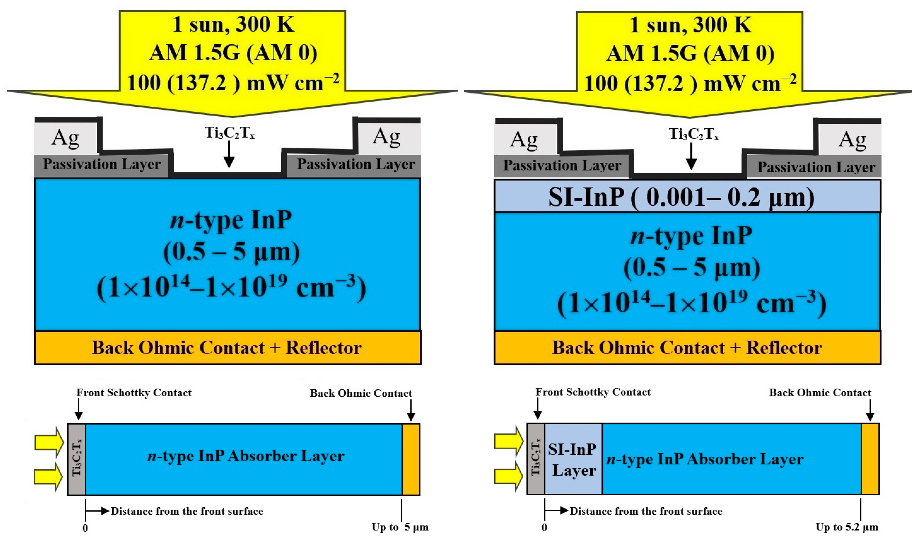
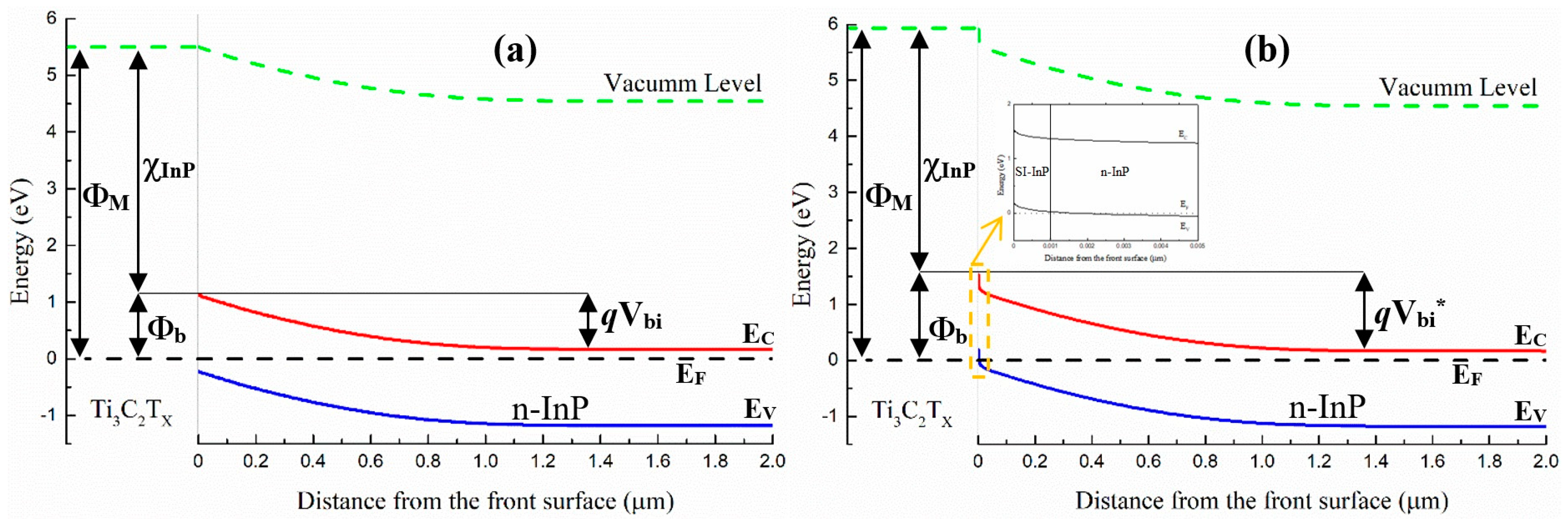
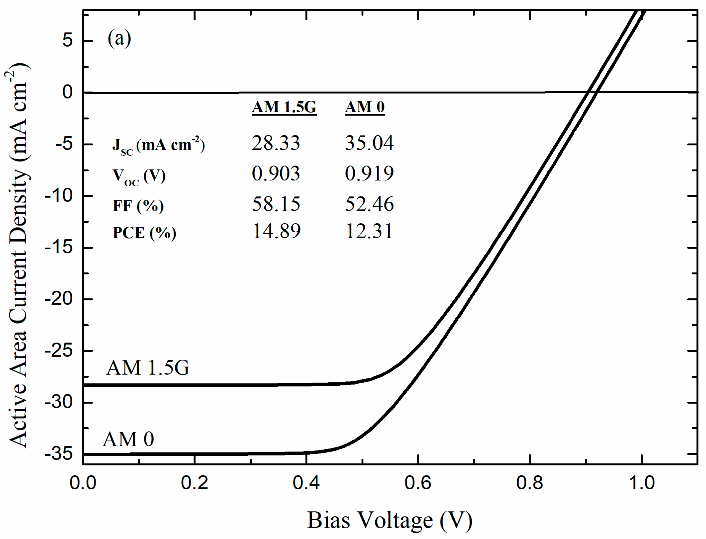
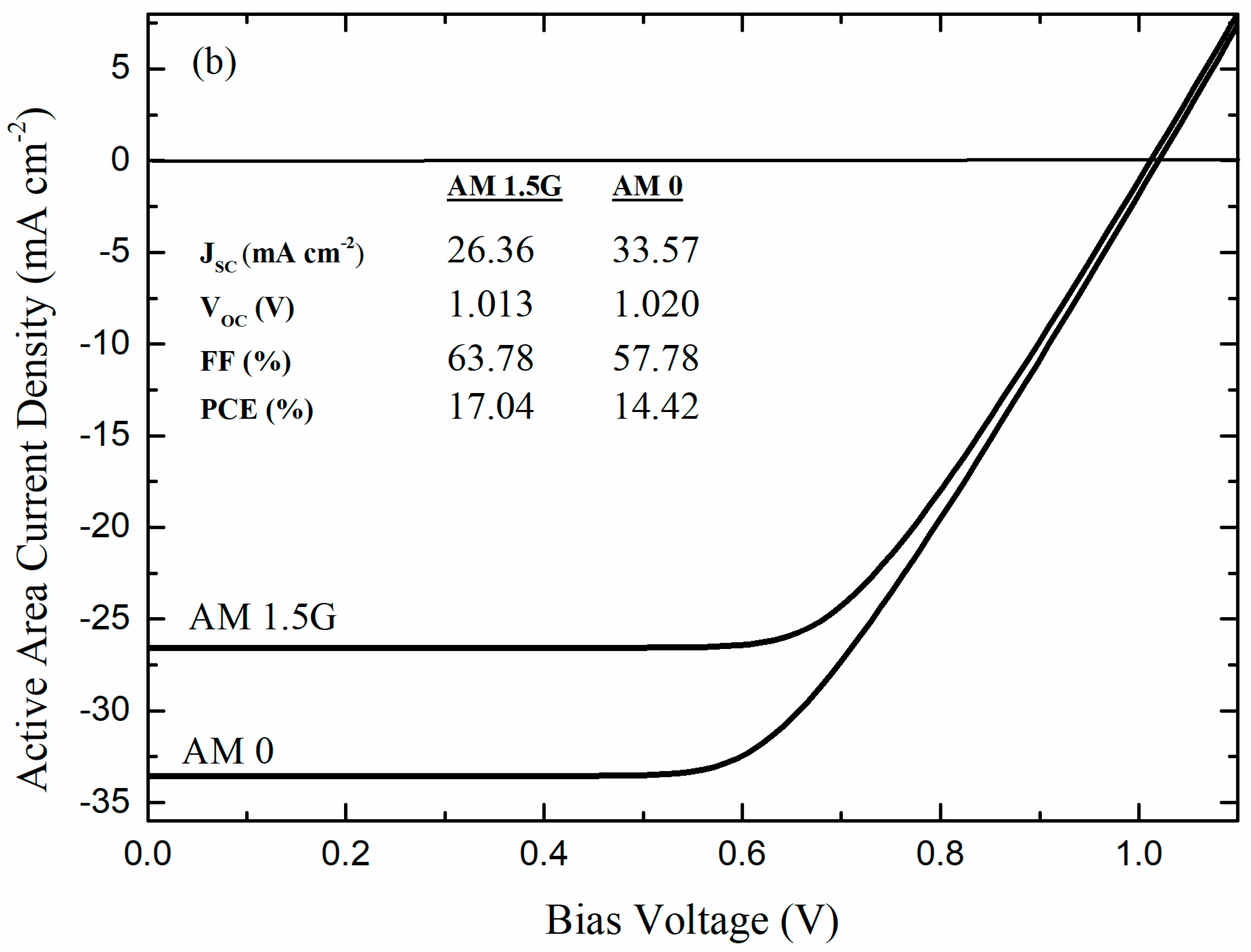
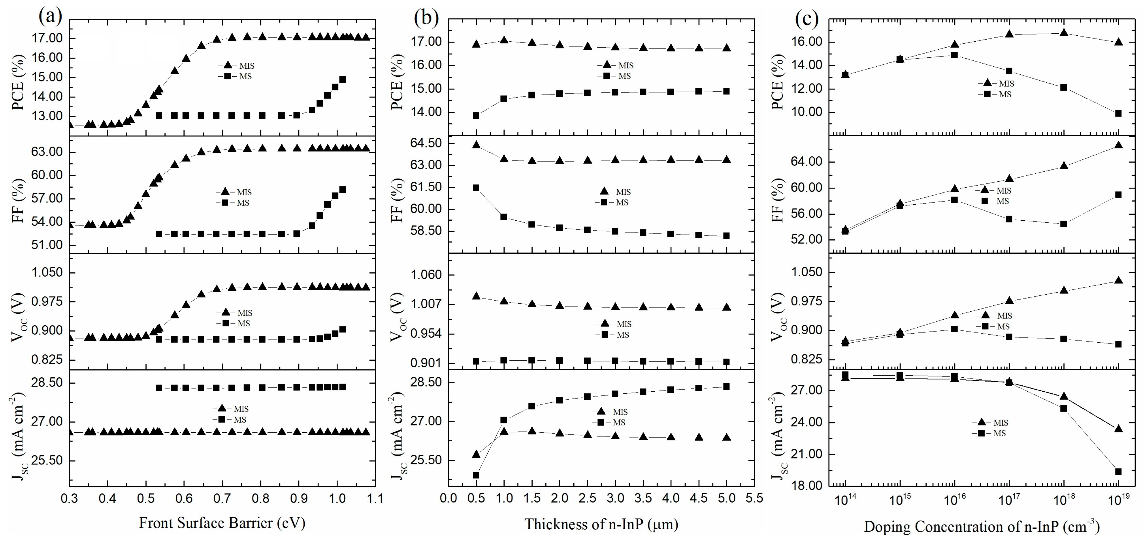
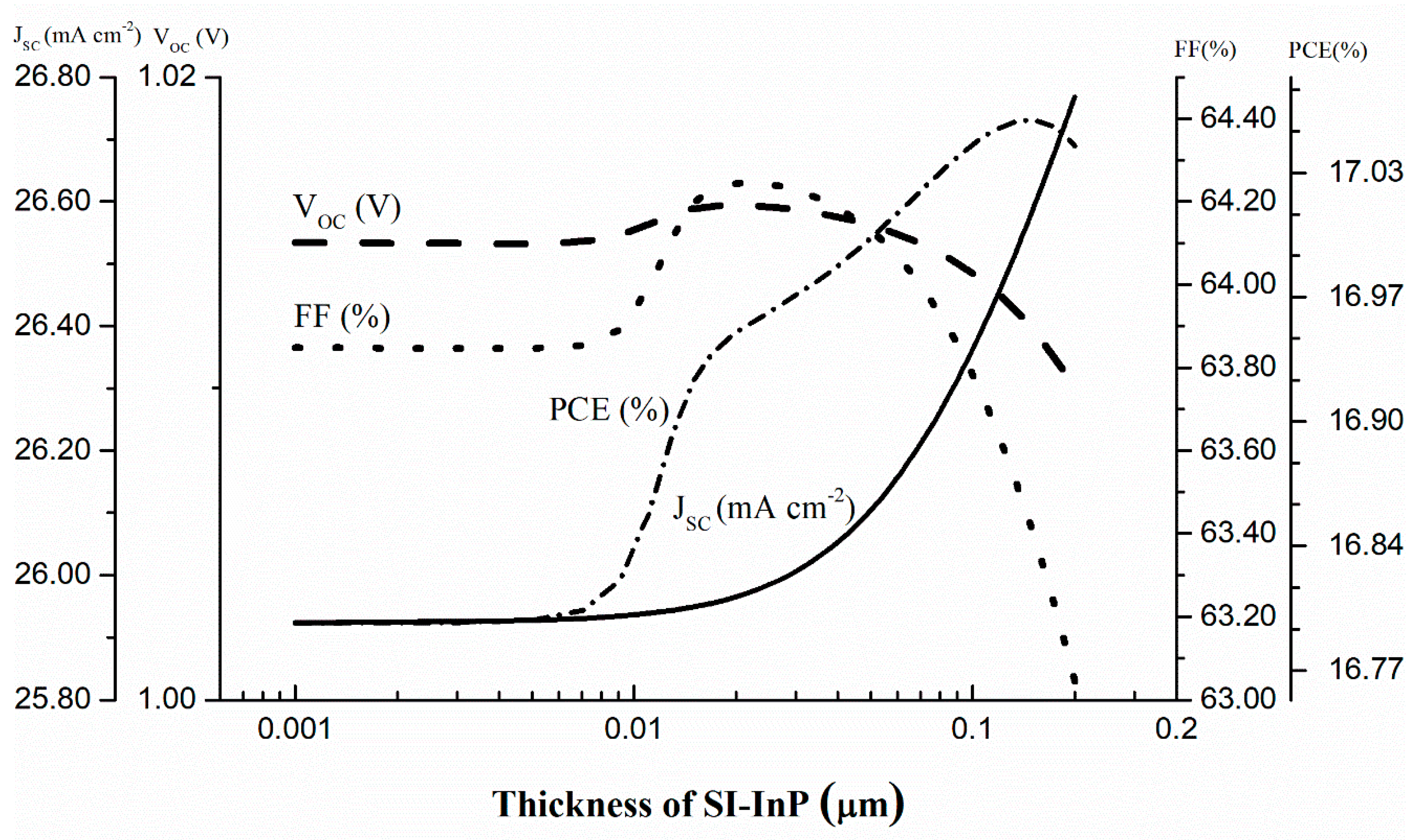
3.1. Optimization of MS and MIS Structures

The Ti3C2Tx work function can be tuned theoretically from ~1.6 eV to ~6.7 eV [52]. However, Si-based and GaAs-based Schottky solar cell experiments have shown work functions ranging from ~5 eV to ~5.5 eV [32,33]. Hence, this range, which corresponds to an expected built-in potential barrier (qVbi) range from ~0.40 eV to ~1.20 eV (ND = 1 × 10¹⁴ − 1 × 1019 cm−3), was considered for optimizing the MS cell. For the MIS cell, the same range is used; nonetheless, this range does not necessarily correspond to the same metal work function range as in the MS structure since the metal in the MIS structure comes into intimate contact with the highly resistive SI-InP interlayer, as opposed to the n-InP layer, with a much lower, nonvarying carrier concentration (~1.2 × 108 cm−3). The optimization for both cells also involved varying the n-InP layer doping concentration (ND) from 1 × 10¹⁴ to 1 × 1019 cm−3 and the n-InP layer thickness from 0.5 to 5 μm while keeping the remaining parameters fixed, as specified in Table 2. The SI-InP layer’s thickness was varied from 0.001 to 0.2 μm for the MIS solar cell structure. Table 3 presents the optimized parameters for both structures, assuming a 300 K ambient temperature under the AM 1.5G and AM 0 spectra.
For the MS solar cell simulated under both solar spectra, the optimal combination of qVbi and ND in Table 3 corresponds to the imposed upper limit of Ti3C2Tx’s work function of ~5.5 eV, as expected. However, when the MS solar cell is simulated under the AM 0 solar spectrum, it requires half the thickness and a higher doping concentration to achieve the highest PCE compared to the one simulated under the AM 1.5G solar spectrum. The optimum base doping concentration value of 1 × 1017 cm−3 aligns with a previous study on p+/n InP-based homojunctions designed for space applications [53]. These outcomes are encouraging, especially if this structure is, for instance, used for unmanned aerial vehicle UAV applications, where weight and high radiation are significant concerns. Using less material would also mean lower costs, and higher doping concentrations are beneficial for enhanced radiation hardness in InP [41].
The situation differs for the MIS solar cell, where the optimum values for qVbi, ND, and the n-InP layer thickness are identical under both solar spectra. The optimum qVbi value of ~0.865 eV is way below the maximum (1.135 eV) for an ND of 1 × 1018 cm−3. Surprisingly, the performance is hardly affected beyond this point, unlike the situation with the MS structure. Note that the ideal thickness for the MIS solar cell structure (1.15 μm) is significantly lower than the MS structure thickness (5 μm) by almost a factor of five under the AM 1.5G spectrum and is less than one-half of the MS structure thickness (2.5 μm) under AM 0. This implies that solar arrays based on MIS structures will have higher specific power (W/Kg), making them more attractive for weight-sensitive applications [54].
The J-V characteristics simulated under AM 1.5G and AM 0 solar spectra for MS and MIS Schottky structures, along with performance data, are shown in Figure 4. Both structures performed better under AM 1.5G compared to AM 0, which agrees with previous investigations on the performance of InP-based solar cells under both spectra [53,55]. The introduction of SI-InP enhanced the open circuit voltage (VOC) under AM 1.5G; however, it has led to lower short circuit current densities (Jsc) in the MIS structure. Despite this, the MIS structure has a higher fill factor (FF) and PCE under both spectra than the MS structure.

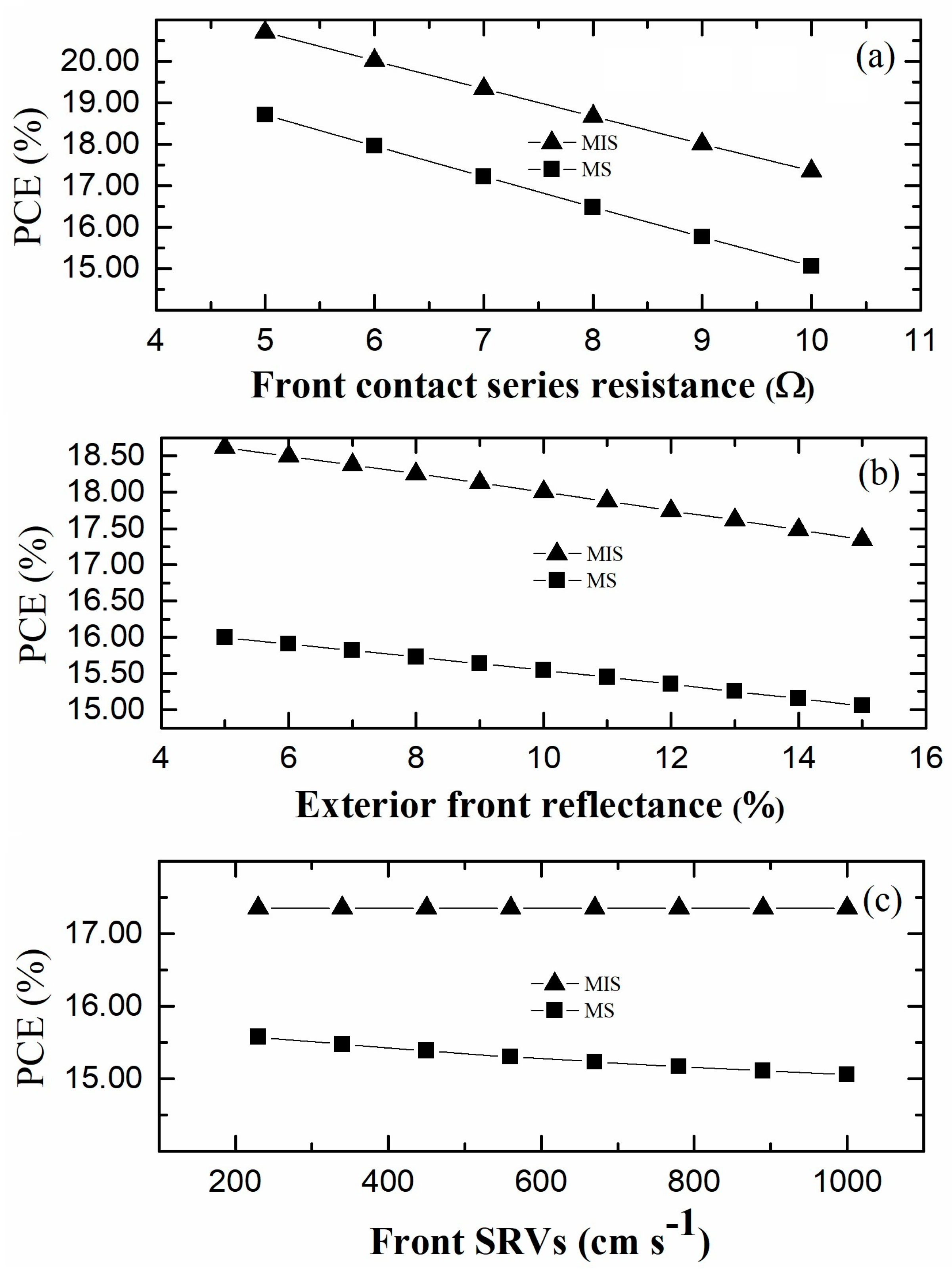
3.2. Performance Sensitivity to Optimization Parameters

Since this work is primarily concerned with designing low-cost InP-based Schottky solar cells for terrestrial applications, the simulation results shown in Figure 5 assume only the AM 1.5G spectrum to illustrate the performance sensitivity of the optimized MS and MIS structures to changes in the optimized parameters listed in Table 3.
A specific threshold front surface barrier value exists for both structures, where the photovoltaic action diminishes due to the absence of (or very low) Φb for a given doping concentration. This corresponds to a metal with a work function comparable to or lower than an n-type semiconductor. According to the ideal MS junction’s theory, this leads to the formation of an ohmic contact rather than a Schottky contact to the n-type semiconductor. The threshold qVbi values are ~0.55 eV and ~0.1 eV for the MS and MIS structures. As displayed in Figure 5a, the performance of the MS structure is almost unchanged for qVbi < ~0.90 eV, and afterward, the PCE and FF increase to their maximum values (14.89% and 58.15%), due to the improvement in VOC. In the MIS structure, improvement in PCE and FF happens earlier, at qVbi of ~0.45 eV. As of the influence of the n-InP absorber thickness (Figure 5b), the PCE of the MS structure noticeably increases at thicknesses <~2 μm and keeps increasing very slightly afterward, but it starts to decrease beyond 15 μm (outside the range shown). For the MIS structure, the improvement in PCE due to JSC occurs in the n-InP thickness range of 0.5–1 μm, slightly decreases until 3 μm, and then remains constant until 15 μm, after which it decreases slightly (outside the range shown). Figure 5c depicts the influence of n-InP absorber doping concentration (ND) on both structures, where JSC starts to decrease at ND > 1 × 1016 cm−3. However, this decrease is offset by a continuous increase in VOC along the whole range of ND in the MIS structure. The situation is different for the MS structure, since VOC starts decreasing at ND > 1 × 1016 cm−3, which causes the PCE to reach its maximum earlier than the MIS structure. Figure 6 shows the influence of SI-InP layer thickness on the MIS structure’s performance. The increase in JSC for thicknesses >0.01 μm is negated by the decrease in VOC and the FF, leading to a delayed decrease in PCE after 0.1 μm.

3.3. Possible Performance Gains

It is important to remember that the demonstrated results are based on various constraints, derived from reported measurements in pioneering experimental studies of Schottky solar cells with MXene TCEs [32,33]. These constraints include front contact series resistance of 10 Ω, exterior front reflectance of 15%, and front SRV of 1 × 103 cm s−1. Additionally, all the simulations performed so far assume the absence of a back surface reflector.
The performance of both MS and MIS Mxene/n-InP Schottky solar cells can be significantly improved if the above constraints can be relaxed. However, to be realistic, experimental evidence must justify such relaxation. The 10 Ω front contact series resistance is based on the reported series resistance for MXene/GaAs devices with the highest efficiency. It is assumed that the MXene thin film contacting the GaAs absorber is the device component contributing dominantly to this resistance. Regardless, the experimental measurements of both studies investigating MXene/Si and MXene/GaAs contacts showed consequential variability in terms of the measured sheet resistance of the deposited MXene thin film, which is a function of thickness, oxidation, chemical treatment/doping, and top metal grid mesh. This fact suggests that further experimentation with this novel material could decrease the series resistance, as observed in graphene and other 2D materials [28,56,57].
It has been demonstrated that traditional ARCs were experimentally optimized to produce an average reflectance of about 3.5% in InP-based solar cells, while novel optical management techniques have achieved values below this threshold [58,59]. Additionally, rear back surface reflectors reflecting over 90% of long wavelength photons (λ > 900 nm) using double layer Ag/Cu contacts were demonstrated for GaInNAs solar cells, leading to enhanced photocurrent and, consequently, external quantum efficiency (EQE) [60].
The same argument of experimental variability is applied to the assumed value of SRV of 1 × 103 cm s−1 in the simulations. As discussed in Section 2, the value of SRV can be reduced to as low as 200 cm s−1, depending on the InP growth method and surface quality/treatments [44].
Suppose both structures, as shown in Figure 2, incorporate an effective back surface reflector capable of reflecting 90% of non-absorbed solar radiation in the first pass; then, this can be simulated in PC1D by assuming a rear internal diffuse reflectance of 90% in the first and subsequent bounces. Figure 7 shows the results of the simulations, which reveal the projected enhancement in PCE for both MS and MIS structures as a result of improvement in the parameters above.
Based on the data presented in Figure 7, it is evident that the front contact series resistance and exterior front reflectance significantly impact the PCE of both cell structures. On the other hand, the front surface recombination velocities (SRVs) have a negligible effect on the PCE of the MIS structure, unlike the MS structure. However, the effect of this parameter is minor when compared to the impact of front contact series resistance and exterior front reflectance. The front contact’s series resistance value could be improved experimentally, but 5 Ω was chosen as a realistic minimum value for now to avoid performance overestimation (Figure 7a), as mature solar cell technologies typically have area-normalized series resistance values that are much less than 5 Ωcm2 [61]. The J-V characteristics, simulated under the AM 1.5G solar spectrum for the MS and MIS structures after considering the improved potential gain parameters, are shown in Figure 8, along with performance data. Assuming a front contact series resistance of 5 ohms, a front surface reflectance of 5%, and front SRVs of 200 cm s−1, these favorable figures are achieved by using the optimum parameter values, as listed in Table 3. All other parameters are fixed, as specified in Table 2.

4. Conclusions

A detailed analysis of MXene/n-InP Schottky barrier solar cells designed using PC1D software is presented in this paper. The proposed simple design, in which the functional Ti3C2Tx MXene TCE material is deposited using low-temperature solution-processing methods on the thin InP absorber layer can yield high PCEs, possibly over 20%, in both MS and MIS structures, as per the discussed simulation results. These qualities would enable these Schottky barrier solar cells to compete with their InP-based p/n homojunction counterparts in terms of cost-effectiveness. Combining the simpler MS or MIS structures with the anticipated, more affordable InP growth methods [62], such as thin-film vapor-liquid-solid (TF-VLS) growth [63], could lessen the gap and make InP more competitive in the terrestrial market. This is especially true for niche applications that require lightweight and radiation-hard solar photovoltaic cells.

Funding

This research received no external funding.

Data Availability Statement

The original contributions presented in the study are included in the article, further inquiries can be directed to the corresponding author.

Acknowledgments

The researcher would like to thank the Deanship of Scientific Research, Qassim University for funding the publication of this project.

Conflicts of Interest

The author declares no conflicts of interest.

References

  1. Ang, T.-Z.; Salem, M.; Kamarol, M.; Das, H.S.; Nazari, M.A.; Prabaharan, N. A comprehensive study of renewable energy sources: Classifications, challenges and suggestions. Energy Strategy Rev. 2022, 43, 100939. [Google Scholar] [CrossRef]
  2. Chee, A.K.-W. On current technology for light absorber materials used in highly efficient industrial solar cells. Renew. Sustain. Energy Rev. 2023, 173, 113027. [Google Scholar] [CrossRef]
  3. Yamaguchi, M. Radiation-resistant solar cells for space use. Sol. Energy Mater. Sol. Cells 2001, 68, 31–53. [Google Scholar] [CrossRef]
  4. Matthew, P.L.; Myles, A.S.; John, F.G.; Robert, J.W. Analytical modeling of III-V solar cells close to the fundamental limit. In Proceedings of the SPIE OPTO Conference, San Francisco, CA, USA, 7 March 2014; p. 898114. [Google Scholar]
  5. Gupta, B.; Shehata, M.M.; Lee, Y.; Black, L.E.; Ma, F.; Hoex, B.; Jagadish, C.; Tan, H.H.; Karuturi, S. Unveiling the Role of H2 Plasma for Efficient InP Solar Cells. Sol. RRL 2023, 7, 2200868. [Google Scholar] [CrossRef]
  6. Ward, J.S.; Remo, T.; Horowitz, K.; Woodhouse, M.; Sopori, B.; VanSant, K.; Basore, P. Techno-economic analysis of three different substrate removal and reuse strategies for III-V solar cells. Prog. Photovolt. Res. Appl. 2016, 24, 1284–1292. [Google Scholar] [CrossRef]
  7. Wanlass, M.U.S. Systems and Methods for Advanced Ultra-High-Performance InP Solar Cells. U.S. Patent 9,590,131B2, 7 March 2017. [Google Scholar]
  8. Green, M.A.; Dunlop, E.D.; Yoshita, M.; Kopidakis, N.; Bothe, K.; Siefer, G.; Hao, X. Solar cell efficiency tables (version 62). Prog. Photovolt. Res. Appl. 2023, 31, 651–663. [Google Scholar] [CrossRef]
  9. Rühle, S. Tabulated values of the Shockley–Queisser limit for single junction solar cells. Sol. Energy 2016, 130, 139–147. [Google Scholar] [CrossRef]
  10. Sree Harsha, K.S.; Bachmann, K.J.; Schmidt, P.H.; Spencer, E.G.; Thiel, F.A. n-indium tin oxide/p-indium phosphide solar cells. Appl. Phys. Lett. 1977, 30, 645–646. [Google Scholar] [CrossRef]
  11. Coutts, T.J.; Pearsall, N.M.; Tarricone, L. The influence of input power on the performance of rf sputtered ITO/InP solar cells. J. Vac. Sci. Technol. B Microelectron. Process. Phenom. 1984, 2, 140–144. [Google Scholar] [CrossRef]
  12. Li, X.; Wanlass, M.W.; Gessert, T.A.; Emery, K.A.; Coutts, T.J. High-efficiency indium tin oxide/indium phosphide solar cells. Appl. Phys. Lett. 1989, 54, 2674–2676. [Google Scholar] [CrossRef]
  13. Rosenwaks, Y.; Li, X.; Coutts, T.J. Characterization of heat-treated ITO/InP solar cells. J. Vac. Sci. Technol. A 1997, 15, 2354–2358. [Google Scholar] [CrossRef]
  14. Yoshikawa, A.; Sakai, Y. High efficiency n-CdS/p-InP solar cells prepared by the close-spaced technique. Solid-State Electron. 1977, 20, 133–137. [Google Scholar] [CrossRef]
  15. Bettini, M.; Bachmann, K.J.; Buehler, E.; Shay, J.L.; Wagner, S. Preparation of CdS/InP solar cells by chemical vapor deposition of CdS. J. Appl. Phys. 1977, 48, 1603–1606. [Google Scholar] [CrossRef]
  16. Purica, M.; Budianu, E.; Rusu, E.; Arabadji, P. Electrical properties of the CdS/InP heterostructures for photovoltaic applications. Thin Solid Film. 2006, 511–512, 468–472. [Google Scholar] [CrossRef]
  17. Yin, X.; Battaglia, C.; Lin, Y.; Chen, K.; Hettick, M.; Zheng, M.; Chen, C.-Y.; Kiriya, D.; Javey, A. 19.2% Efficient InP Heterojunction Solar Cell with Electron-Selective TiO2 Contact. ACS Photonics 2014, 1, 1245–1250. [Google Scholar] [CrossRef]
  18. Raj, V.; dos Santos, T.S.; Rougieux, F.; Vora, K.; Lysevych, M.; Fu, L.; Mokkapati, S.; Tan, H.H.; Jagadish, C. Indium phosphide based solar cell using ultra-thin ZnO as an electron selective layer. J. Phys. D Appl. Phys. 2018, 51, 395301. [Google Scholar] [CrossRef]
  19. Raj, V.; Rougieux, F.; Fu, L.; Tan, H.H.; Jagadish, C. Design of Ultrathin InP Solar Cell Using Carrier Selective Contacts. IEEE J. Photovolt. 2020, 10, 1657–1666. [Google Scholar] [CrossRef]
  20. Kamimura, K.; Suzuki, T.; Kunioka, A. InP (MIS) Schottky Barrier Solar Cells. Jpn. J. Appl. Phys. 1980, 19, 203. [Google Scholar] [CrossRef]
  21. Pande, K.P. Characteristics of MOS solar cells built on (n-type) InP substrates. IEEE Trans. Electron Devices 1980, 27, 631–634. [Google Scholar] [CrossRef]
  22. Kamimura, K.; Suzuki, T.; Kunioka, A. Metal-insulator semiconductor Schottky-barrier solar cells fabricated on InP. Appl. Phys. Lett. 1981, 38, 259–261. [Google Scholar] [CrossRef]
  23. Li, Y.; Yu, M.; Cheng, Q. Improved performance of graphene/n-GaAs heterojunction solarcells by introducing an electron-blocking/hole-transporting layer. Mater. Res. Express 2019, 6, 016202. [Google Scholar] [CrossRef]
  24. Fonash, S.J. Solar Cell Device Physics; Elsevier Inc.: Boston, MA, USA, 2010; p. 381. [Google Scholar]
  25. Har-Lavan, R.; Cahen, D. 40 Years of Inversion Layer Solar Cells: From MOS to Conducting Polymer/Inorganic Hybrids. IEEE J. Photovolt. 2013, 3, 1443–1459. [Google Scholar] [CrossRef]
  26. Kuphal, E. Low resistance ohmic contacts to n- and p-InP. Solid-State Electron. 1981, 24, 69–78. [Google Scholar] [CrossRef]
  27. Alnassar, M.S.N. Discovering new pathways to improved performance of TFSA-doped single-layer graphene/n-Si Schottky barrier solar cells: A detailed numerical study. Optik 2024, 299, 171640. [Google Scholar] [CrossRef]
  28. Kong, X.; Zhang, L.; Liu, B.; Gao, H.; Zhang, Y.; Yan, H.; Song, X. Graphene/Si Schottky solar cells: A review of recent advances and prospects. RSC Adv. 2019, 9, 863–877. [Google Scholar] [CrossRef]
  29. Yin, X.; Tang, C.S.; Zheng, Y.; Gao, J.; Wu, J.; Zhang, H.; Chhowalla, M.; Chen, W.; Wee, A.T.S. Recent developments in 2D transition metal dichalcogenides: Phase transition and applications of the (quasi-)metallic phases. Chem. Soc. Rev. 2021, 50, 10087–10115. [Google Scholar] [CrossRef]
  30. Naguib, M.; Kurtoglu, M.; Presser, V.; Lu, J.; Niu, J.; Heon, M.; Hultman, L.; Gogotsi, Y.; Barsoum, M.W. Two-Dimensional Nanocrystals Produced by Exfoliation of Ti3AlC2. Adv. Mater. 2011, 23, 4248–4253. [Google Scholar] [CrossRef]
  31. Guo, Z.; Gao, L.; Xu, Z.; Teo, S.; Zhang, C.; Kamata, Y.; Hayase, S.; Ma, T. High Electrical Conductivity 2D MXene Serves as Additive of Perovskite for Efficient Solar Cells. Small 2018, 14, 1802738. [Google Scholar] [CrossRef]
  32. Yu, L.; Bati, A.S.R.; Grace, T.S.L.; Batmunkh, M.; Shapter, J.G. Ti3C2Tx (MXene)-Silicon Heterojunction for Efficient Photovoltaic Cells. Adv. Energy Mater. 2019, 9, 1901063. [Google Scholar] [CrossRef]
  33. Zhang, Z.; Lin, J.; Sun, P.; Zeng, Q.; Deng, X.; Mo, Y.; Chen, J.; Zheng, Y.; Wang, W.; Li, G. Air-stable MXene/GaAs heterojunction solar cells with a high initial efficiency of 9.69%. J. Mater. Chem. A 2021, 9, 16160–16168. [Google Scholar] [CrossRef]
  34. Clugston, D.A.; Basore, P.A. PC1D version 5: 32-bit solar cell modeling on personal computers. In Proceedings of the Conference Record of the Twenty Sixth IEEE Photovoltaic Specialists Conference, Anaheim, CA, USA, 29 September–3 October 1997; pp. 207–210. [Google Scholar]
  35. Kc, D.; Shah, D.K.; Akhtar, M.S.; Park, M.; Kim, C.Y.; Yang, O.B.; Pant, B. Numerical Investigation of Graphene as a Back Surface Field Layer on the Performance of Cadmium Telluride Solar Cell. Molecules 2021, 26, 3275. [Google Scholar] [CrossRef] [PubMed]
  36. Thirunavukkarasu, G.S.; Seyedmahmoudian, M.; Chandran, J.; Stojcevski, A.; Subramanian, M.; Marnadu, R.; Alfaify, S.; Shkir, M. Optimization of Mono-Crystalline Silicon Solar Cell Devices Using PC1D Simulation. Energies 2021, 14, 4986. [Google Scholar] [CrossRef]
  37. Parajuli, D.; Kc, D.; Khattri, K.B.; Adhikari, D.R.; Gaib, R.A.; Shah, D.K. Numerical assessment of optoelectrical properties of ZnSe–CdSe solar cell-based with ZnO antireflection coating layer. Sci. Rep. 2023, 13, 12193. [Google Scholar] [CrossRef] [PubMed]
  38. Alnassar, M.S.N. Utilization of open-source software in teaching the physics of P-N diodes. Comput. Appl. Eng. Educ. 2023, 31, 867–883. [Google Scholar] [CrossRef]
  39. Jain, R.K.; Flood, D.J. Effects of recombination parameters in p+n indium phosphide solar cells. Sol. Energy Mater. Sol. Cells 1997, 45, 51–55. [Google Scholar] [CrossRef]
  40. Piprek, J.; Boer, K.W. InP solar cell improvement by inverse delta-doping. In Proceedings of the First IEEE World Conference on Photovoltaic Energy Conversion—WCPEC (A Joint Conference of PVSC, PVSEC and PSEC), Waikoloa, HI, USA, 5–9 December 1994; pp. 1818–1821. [Google Scholar]
  41. Weinberg, I. InP solar cells for use in space. Sol. Cells 1990, 29, 225–244. [Google Scholar] [CrossRef]
  42. Bugajski, M.; Lewandowski, W. Concentration-dependent absorption and photoluminescence of n-type InP. J. Appl. Phys. 1985, 57, 521–530. [Google Scholar] [CrossRef]
  43. Sotoodeh, M.; Khalid, A.H.; Rezazadeh, A.A. Empirical low-field mobility model for III–V compounds applicable in device simulation codes. J. Appl. Phys. 2000, 87, 2890–2900. [Google Scholar] [CrossRef]
  44. Pearsall, T.P. Properties, Processing and Applications of Indium Phosphide; INSPEC/The Institution of Electrical Engineers: London, UK, 2000; p. 300. [Google Scholar]
  45. Vidimari, F.; Pellegrino, S.; Caldironi, M.; Paola, A.D.; Chen, R. High resistivity layers in InP obtained by Co or Fe ion implantation and LPE regrowth. In Proceedings of the Third International Conference Indium Phosphide and Related Materials, Cardiff, UK, 8–11 April 1991; pp. 500–503. [Google Scholar]
  46. Sze, S.M.; Ng, K.K. The Physics of Semiconductor Devices; John Wiley & Sons, Inc.: New York, NY, USA, 2007; p. 815. [Google Scholar]
  47. McIntosh, K.R.; Baker-Finch, S.C. OPAL 2: Rapid optical simulation of silicon solar cells. In Proceedings of the Conference 38th IEEE Photovoltaic Specialists Conference, Austin, TX, USA, 3–8 June 2012; pp. 000265–000271. [Google Scholar]
  48. Palik, E.D. Handbook of Optical Constants of Solids; Academic Press: San Diego, CA, USA, 1985; p. 804. [Google Scholar]
  49. Aspnes, D.E.; Studna, A.A. Dielectric functions and optical parameters of Si, Ge, GaP, GaAs, GaSb, InP, InAs, and InSb from 1.5 to 6.0 eV. Phys. Rev. B 1983, 27, 985–1009. [Google Scholar] [CrossRef]
  50. Schroder, D.K.; Meier, D.L. Solar cell contact resistance—A review. IEEE Trans. Electron Devices 1984, 31, 637–647. [Google Scholar] [CrossRef]
  51. Levinshtein, M.; Rumyantsev, S.; Shur, M. Handbook Series on Semiconductor Parameters; World Scientific Publishing Co. Pte. Ltd.: Singapore, 1996; p. 232. [Google Scholar]
  52. Khazaei, M.; Arai, M.; Sasaki, T.; Ranjbar, A.; Liang, Y.; Yunoki, S. OH-terminated two-dimensional transition metal carbides and nitrides as ultralow work function materials. Phys. Rev. B 2015, 92, 075411. [Google Scholar] [CrossRef]
  53. Jain, R.K.; Flood, D.J. Design modeling of high-efficiency p/sup +/-n indium phosphide solar cells. IEEE Trans. Electron Devices 1993, 40, 224–227. [Google Scholar] [CrossRef]
  54. Brandhorst, H.W.; Flood, D.J. The Past, Present and Future of Space Photovoltaics. In Proceedings of the IEEE 4th World Conference on Photovoltaic Energy Conference, Waikoloa, HI, USA, 7–12 May 2006; pp. 1744–1749. [Google Scholar]
  55. Yahia, A.H.; Wanlass, M.W.; Coutts, T.J. Modeling and simulation of InP homojunction solar cells. In Proceedings of the Conference Record of the Twentieth IEEE Photovoltaic Specialists Conference, Las Vegas, NV, USA, 26–30 September 1988; pp. 702–707. [Google Scholar]
  56. Ding, K.; Zhang, X.; Ning, L.; Shao, Z.; Xiao, P.; Ho-Baillie, A.; Zhang, X.; Jie, J. Hue tunable, high color saturation and high-efficiency graphene/silicon heterojunction solar cells with MgF2/ZnS double anti-reflection layer. Nano Energy 2018, 46, 257–265. [Google Scholar] [CrossRef]
  57. Wang, P.; Li, X.; Xu, Z.; Wu, Z.; Zhang, S.; Xu, W.; Zhong, H.; Chen, H.; Li, E.; Luo, J.; et al. Tunable graphene/indium phosphide heterostructure solar cells. Nano Energy 2015, 13, 509–517. [Google Scholar] [CrossRef]
  58. Keavney, C.J.; Spitzer, M.B. Indium phosphide solar cells made by ion implantation. Appl. Phys. Lett. 1988, 52, 1439–1440. [Google Scholar] [CrossRef]
  59. Goldman, D.A.; Murray, J.; Munday, J.N. Nanophotonic resonators for InP solar cells. Opt. Express 2016, 24, A925–A934. [Google Scholar] [CrossRef] [PubMed]
  60. Aho, T.; Aho, A.; Tukiainen, A.; Polojärvi, V.; Salminen, T.; Raappana, M.; Guina, M. Enhancement of photocurrent in GaInNAs solar cells using Ag/Cu double-layer back reflector. Appl. Phys. Lett. 2016, 109, 251104. [Google Scholar] [CrossRef]
  61. McEvoy, A.; Castaner, L.; Markvart, T. Solar Cells: Materials, Manufacture and Operation; Elsevier Inc.: London, UK, 2012. [Google Scholar]
  62. Greenaway, A.L.; Boucher, J.W.; Oener, S.Z.; Funch, C.J.; Boettcher, S.W. Low-Cost Approaches to III–V Semiconductor Growth for Photovoltaic Applications. ACS Energy Lett. 2017, 2, 2270–2282. [Google Scholar] [CrossRef]
  63. Zheng, M.; Horowitz, K.; Woodhouse, M.; Battaglia, C.; Kapadia, R.; Javey, A. III-Vs at scale: A PV manufacturing cost analysis of the thin film vapor–liquid–solid growth mode. Prog. Photovolt. Res. Appl. 2016, 24, 871–878. [Google Scholar] [CrossRef]
Figure 1. Comparison of bandgap narrowing results for different donor concentrations of n-type InP at 300 K [42].
Condensedmatter 09 00017 g001
Figure 2. Schematic representations of MS and MIS MXene/n-InP Schottky solar cells (top) and their equivalent 1D structures simulated in PC1D (bottom).
Condensedmatter 09 00017 g002
Figure 3. Simulation results showing the energy band diagram at equilibrium for the (a) MS and (b) MIS structures (only up to 2 μm is shown for both structures). The inset in (b) shows the effect of the 1 nm SI-InP interlayer on the energy levels within 5 nm from the MI junction in the MIS structure.
Condensedmatter 09 00017 g003
Figure 4. J-V characteristics and performance results for the optimum (a) MS and (b) MIS MXene/n-InP Schottky solar cells.
Condensedmatter 09 00017 g004aCondensedmatter 09 00017 g004b
Figure 5. Performance sensitivity of MS and MIS MXene/n-InP Schottky solar cells to changes in (a) qVbi, (b) n-InP layer thickness, and (c) its doping concentration.
Condensedmatter 09 00017 g005
Figure 6. Effect of SI-InP thickness on the performance of MIS MXene/n-InP Schottky solar cell.
Condensedmatter 09 00017 g006
Figure 7. Potential gain in PCE of MS and MIS MXene/n-InP Schottky solar cells due to improved (a) front contact series resistance, (b) exterior front reflectance, and (c) front SRVs.
Condensedmatter 09 00017 g007
Figure 8. J-V characteristics and performance results for MS and MIS MXene/n-InP Schottky solar cells assuming improved potential gain parameters.
Condensedmatter 09 00017 g008
Table 1. Modified mobility-fitting parameters in PC1D for InP simulations (300 K).
Parameterμmax
(cm2/Vs)
μmin
(cm2/Vs)
Nref
(cm−3)
αβ1β2β3β4vsat
(cm/s)
Electrons52004003 × 10170.470−23.2502.6 × 107
Holes170104.87 × 10170.470−2302.6 × 107
Table 2. Parameters used for the initial simulation of MS and MIS MXene/n-InP solar cells.
Device Parameters
ParameterValueReference
Front surface barrier (qVbi) 0.956 eV *Ti3C2Tx TCE thin film [33]
Exterior front reflectance15% **According to [33]
Front contact resistance10 Ω **Ti3C2Tx TCE thin film [33]
Back contact resistance0.1 ΩAssuming good ohmics [50]
Region Parameters (n-InP)
ParameterValueReference
Bandgap1.344 eVAccording to [51]
Electron affinity4.38 eVAccording to [51]
Thickness3 μm *Initial simulation
MobilityVariableAccording to [43]
Dielectric constant12.61According to [51]
Refractive indexVariable(using inp.inr file)
Absorption coefficientVariable(using inp300.abs file)
Intrinsic concentration (300 K)1.3 × 107 cm−3According to [51]
Doping concentration (ND)1 × 1015 cm−3 *Initial simulation
Bulk recombination lifetimes1 μsAccording to [44]
Front SRVs (Sn and Sp)1000 cm s−1 **According to [44]
Back SRVs (Sn and Sp)1000 cm s−1According to [44]
Region Parameters (SI-InP)
ParameterValueReference
Thickness0.001 μm *Initial simulation
Resistivity10 MΩ·cmSemi-insulating layer [45]
Front SRVs (Sn and Sp)1000 cm s−1 **According to [44]
Excitation Parameters
ParameterValue
SpectrumAM 1.5G and AM 0
Constant intensity100 mW cm−2 and 137.2 mW cm−2
Temperature300 K
The parameter value must be a negative number in PC1D to invoke upward band bending. * These parameters are varied, while others are kept constant to find the optimum MS (MIS) structures. ** After optimization, these parameters are modified to explore possible performance gains.
Table 3. Optimum parameter values for MXene/n-InP MS and MIS Schottky solar cells.
PC1D Design ParameterSchottky Barrier Solar Cell Structure
MSMIS
AM 1.5GAM 0AM 1.5GAM 0
Front surface barrier qVbi (eV)1.0151.0750.8650.865
Thickness of n-InP (μm)52.511
Doping conc. of n-InP (cm−3)1 × 10161 × 10171 × 10181 × 1018
Thickness of SI-InP (μm)--0.150.1
Disclaimer/Publisher’s Note: The statements, opinions and data contained in all publications are solely those of the individual author(s) and contributor(s) and not of MDPI and/or the editor(s). MDPI and/or the editor(s) disclaim responsibility for any injury to people or property resulting from any ideas, methods, instructions or products referred to in the content.

