
Impact of Solid-State Charge Injection on Spectral Photoresponse of NiO/Ga2O3 p–n Heterojunction
 , , , , , and
Abstract
:1. Introduction
- Flame detection: Solar-blind photodetectors can be used to detect flames, which emit UV light, even in the presence of sunlight or other visible light sources. This makes them useful for fire safety applications, such as in industrial plants and aircraft.
- Missile launch detection: Solar-blind photodetectors can be used to detect missile launches, which also emit UV light. This makes them useful for military and security applications.
- Astronomical observation: Solar-blind photodetectors can be used to observe astronomical objects in the UV spectrum, which is not possible with traditional optical telescopes.
- Ozone layer monitoring: Solar-blind photodetectors can be used to monitor the ozone layer, which absorbs UV light. This information can be used to track the depletion of the ozone layer and to predict the effects of climate change.
2. Experimental Section
3. Results and Discussion
- Charge injection from the electron beam of SEM and forward bias injection, reported in this work, demonstrate similarities in terms of their impact on minority carrier diffusion length in gallium oxide. As was already mentioned above, forward bias application to the NiO/Ga2O3 p–n junction results in a decrease in the potential barrier (~1.03 V for Vbi [27]) at the interface of two semiconducting layers. As a result, the holes from p-niO are injected into n-Ga2O3 and likely become captured by meta-stable traps. Although the exact energetic location for these possible traps is yet unknown, ref. [32] recently reported a trapping level for holes in n-type Ga2O3 located 140 meV above the top of the valence band. This level was revealed via the deep level transient spectroscopy (DLTS) technique while studying hole injection via trap-assisted tunneling from p+-NiO into n-Ga2O3 under forward bias. Capturing injected charge carriers on meta-stable energetic levels prevents the recombination of light-induced non-equilibrium carriers in n-type gallium oxide through these levels. As a result, the non-equilibrium carriers remain in the respective valence and conduction bands of gallium oxide for longer periods, in turn leading to larger carrier lifetime, τ, and therefore longer diffusion length, L.
- Although L was not directly measured for the structure shown in Figure 1 and studied in the experiments reported here, it is logical to assume that forward bias charge injection leads to an increase in minority hole diffusion length in the 10-μm-thick n-type Ga2O3 epitaxial layer in agreement with the mechanism described above and in ref. [29]. Because the concentration of majority carriers in n-Ga2O3 is two orders of magnitude lower than that of p-niO, the built-in electric field, employed for non-equilibrium carrier charge separation, is mostly localized in the 10-μm-thick n-type gallium oxide epitaxial layer (extends ~180 nm from the NiO/Ga2O3 interface into 10 μm-thick n-Gallium Oxide [27]). Therefore, the diffusion length for minority holes in this layer are of primary importance.
- According to ref. [36], which studied the absorption of UV radiation (at 250 nm) in the NiO/Ga2O3 heterojunction, more than 80% of the light, shining vertically on the Ni/Au/NiO stack (cf. Figure 1), is absorbed and therefore does not reach the underlying 10-μm-thick n-type gallium oxide epitaxial layer. As a result, the only portion of 10-μm-thick Si-doped n-Ga2O3, which is not covered by the above Ni/Au contact and NiO bilayer, contributes to the photoresponse. Therefore, the collection of non-equilibrium photoexcited carriers in n-Ga2O3 is lateral, as shown by the centripetal arrows in Figure 1, meaning that the non-equilibrium minority carriers (holes) are mostly swept by the vertical portion of the NiO/Ga2O3 space charge region, which extends laterally (~180 nm) beyond the heterojunction interface.
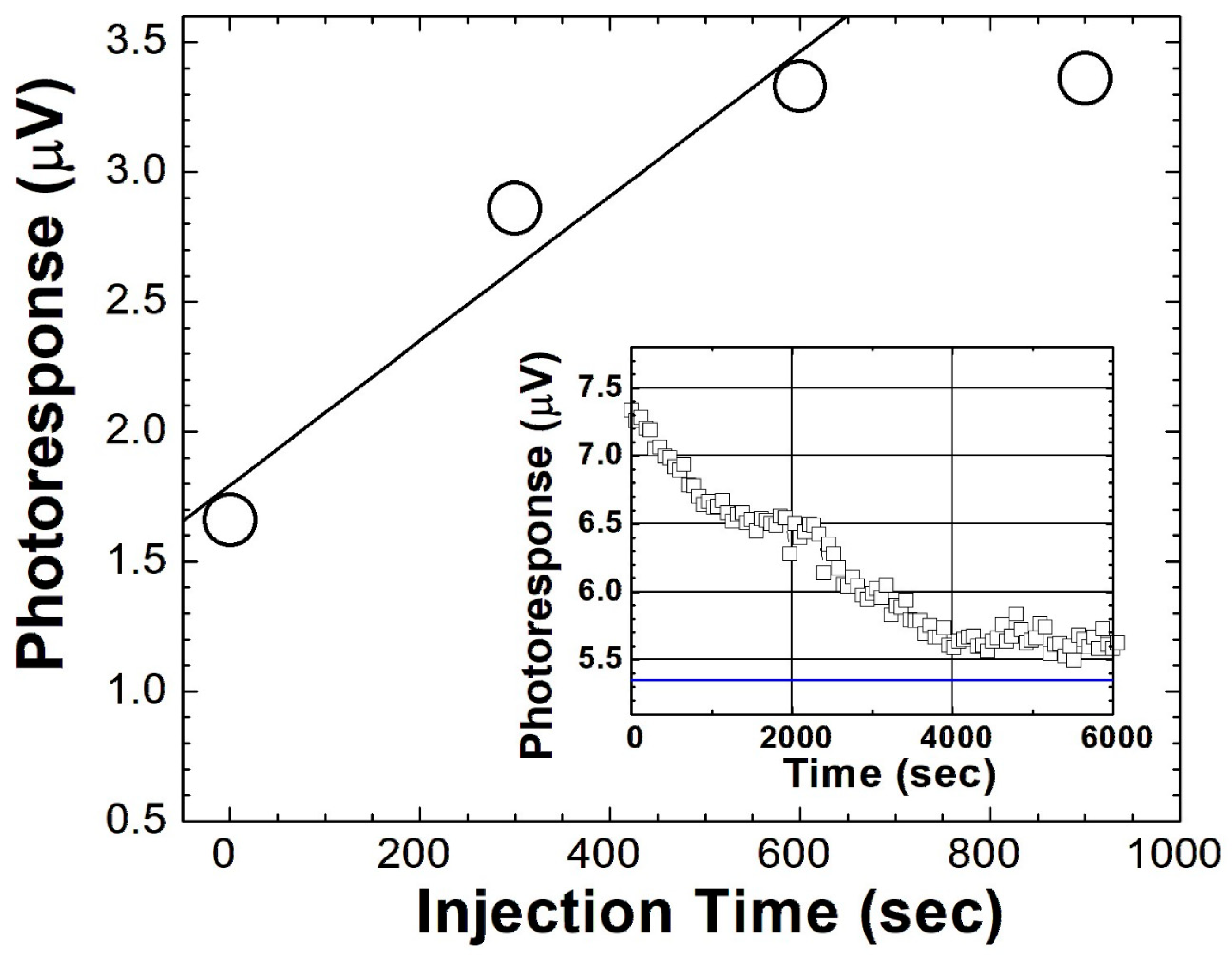
- The minority hole diffusion length, L, measured at room temperature in ref. [27] for n-type Ga2O3 using the electron beam-induced current (EBIC) technique, was reported at ~400 nm prior to electron beam injection. It is generally accepted that light-excited (due to illumination) non-equilibrium carriers, generated within 2L distance from the space-charge region (depletion region), are capable of diffusing without recombination towards the p–n junction, where they are swept by its internal electric field, thus contributing to a photocurrent. Therefore, longer diffusion length due to forward bias charge injection leads to the collection of photogenerated carriers from a larger area of the structure presented in Figure 1, thus enhancing collection (by the p–n heterojunction built-in field) efficiency for minority carriers (holes), and therefore representing the main factor that contributes to larger photoresponse with the increasing duration of forward bias [35].
- It should be noted that the structure in Figure 1 is not optimized as a photodetecting device. Therefore, instead of presenting device’s figures of merit, the relative photoresponse increase is demonstrated in Figure 4, thus serving as the proof of concept. While the responsivity (A/V) dependence on the wavelength is more appropriate for optimized device, the data presented in Figure 4 correspond to the output signal of the lock-in amplifier used for the measurements. Accounting for the lock-in amplifier sensitivity and input impedance, the maximum photocurrent is estimated at several fractions of pA. Fabrication of optimized structures is under way, and they will be studied in future experiments. The figures of merit for the optimized NiO/Ga2O3 hetero p–n junctions, used as photovoltaic detectors, are summarized in ref. [36].

- In the configuration of the structure under test, in which the charge collection occurs laterally (cf. Figure 1 and the discussion outlined above), the photoresponse depends linearly on L, as explained in ref. [37]. Therefore, the linear increase for the peak photoresponse with duration of charge injection is confirmed, rather than revealed (as it is known and expected for the lateral charge collection [37]), in Figure 5. The peak photoresponse after 900 s of charge injection, though shown in Figure 5, is not used for the linear fit, due to a clear saturation.
4. Summary
Author Contributions
Funding
Data Availability Statement
Conflicts of Interest
References
- Kalra, A.; Ul Muazzam, U.; Muralidharan, R.; Raghavan, S.; Nath, D.N. The road ahead for ultrawide bandgap solar-blind UV photodetectors. J. Appl. Phys. 2022, 131, 150901. [Google Scholar] [CrossRef]
- Xie, C.; Lu, X.T.; Tong, X.W.; Zhang, Z.X.; Liang, F.X.; Liang, L.; Luo, L.B.; Wu, Y.C. Recent progress in solar-blind deep-ultraviolet photodetectors based on inorganic ultrawide bandgap semiconductors. Adv. Funct. Mater. 2019, 29, 1806006. [Google Scholar] [CrossRef]
- Kaur, D.; Kumar, M. A Strategic Review on Gallium Oxide Based Deep-Ultraviolet Photodetectors: Recent Progress and Future Prospects. Adv. Opt. Mater. 2021, 9, 2002160. [Google Scholar] [CrossRef]
- Xu, J.; Zheng, W.; Huang, F. Gallium oxide solar-blind ultraviolet photodetectors: A review. J. Mater. Chem. C 2019, 7, 8753. [Google Scholar] [CrossRef]
- Flack, T.J.; Pushpakaran, B.N.; Bayne, S.B. GaN technology for power electronic applications: A review. J. Electron. Mater. 2016, 45, 2673. [Google Scholar] [CrossRef]
- Ionascut-Nedelcescu, A.; Carlone, C.; Houdayer, A.; von Bardeleben, H.J.; Cantin, J.-L.; Raymond, S. Radiation hardness of gallium nitride. IEEE Trans. Nucl. Sci. 2002, 49, 2733. [Google Scholar] [CrossRef]
- Onoda, S.; Hasuike, A.; Nabeshima, Y.; Sasaki, H.; Yajima, K.; Sato, S.I.; Ohshima, T. Enhanced charge collection by single ion strike in AlGaN/GaN HEMTs. IEEE Trans. Nucl. Sci. 2013, 60, 4446. [Google Scholar] [CrossRef]
- Nakamura, S.; Mukai, T.; Senoh, M. High-power GaN pn junction blue-light-emitting diodes. Jpn. J. Appl. Phys. 1991, 30, L1998. [Google Scholar] [CrossRef]
- Kokubun, Y.; Kubo, S.; Nakagomi, S. All-oxide p–n heterojunction diodes comprising p-type NiO and n-type β-Ga2O3. Appl. Phys. Express 2016, 9, 091101. [Google Scholar] [CrossRef]
- Deng, Y.; Yang, Z.; Xu, T.; Jiang, H.; Ng, K.W.; Liao, C.; Su, D.; Pei, Y.; Chen, Z.; Wang, G.; et al. Band alignment and electrical properties of NiO/β-Ga2O3 heterojunctions with different β-Ga2O3 orientations. Appl. Surf. Sci. 2023, 622, 156917. [Google Scholar] [CrossRef]
- Pintor-Monroy, M.I.; Barrera, D.; Murillo-Borjas, B.L.; Ochoa-Estrella, F.J.; Hsu, J.W.P.; Quevedo-Lopez, M.A. Tunable Electrical and Optical Properties of Nickel Oxide (NiOx) Thin Films for Fully Transparent NiOx–Ga2O3 p–n Junction Diodes. ACS Appl. Mater. Interfaces 2018, 10, 38159. [Google Scholar] [CrossRef]
- Xia, X.; Li, J.-S.; Chiang, C.-C.; Yoo, T.J.; Ren, F.; Kim, H.; Pearton, S.J. Annealing temperature dependence of band alignment of NiO/β-Ga2O3. J. Phys. D Appl. Phys. 2022, 55, 385105. [Google Scholar] [CrossRef]
- Gong, H.; Chen, X.; Xu, Y.; Chen, Y.; Ren, F.; Liu, B.; Gu, S.; Zhang, R.; Ye, J. Band Alignment and Interface Recombination in NiO/β-Ga2O3 Type-II pn Heterojunctions. IEEE Trans. Electron Device 2020, 67, 3341. [Google Scholar] [CrossRef]
- Sharma, S.; Zeng, K.; Saha, S.; Singisetti, U. Field-Plated Lateral Ga2O3 MOSFETs With Polymer Passivation and 8.03 kV Breakdown Voltage. IEEE Electron Device Lett. 2020, 41, 836. [Google Scholar] [CrossRef]
- Zhang, J.; Dong, P.; Dang, K.; Zhang, Y.; Yan, Q.; Xiang, H.; Su, J.; Liu, Z.; Si, M.; Gao, J.; et al. Ultra-wide bandgap semiconductor Ga2O3 power diodes. Nat. Commun. 2022, 13, 3900. [Google Scholar] [CrossRef] [PubMed]
- Dong, P.; Zhang, J.; Yan, Q.; Liu, Z.; Ma, P.; Zhou, H.; Hao, Y. 6 kV/3.4 mΩ·cm2 Vertical β-Ga2O3 Schottky Barrier Diode With BV2/Ron,sp Performance Exceeding 1-D Unipolar Limit of GaN and SiC. IEEE Electron Device Lett. 2022, 43, 765. [Google Scholar] [CrossRef]
- Lv, Y.; Wang, Y.; Fu, X.; Dun, S.; Sun, Z.; Liu, H.; Zhou, X.; Song, X.; Dang, K.; Liang, S.; et al. Demonstration of β-Ga2O3 Junction Barrier Schottky Diodes with a Baliga’s Figure of Merit of 0.85 GW/cm2 or a 5A/700 V Handling Capabilities. IEEE Trans. Power Electron. 2021, 36, 6179. [Google Scholar] [CrossRef]
- Liao, C.; Lu, X.; Xu, T.; Fang, P.; Deng, Y.; Luo, H.; Wu, Z.; Chen, Z.; Liang, J.; Pei, Y.; et al. Optimization of NiO/β-Ga2O3 Heterojunction Diodes for High-Power Application. IEEE Trans. Electron Device 2022, 69, 5722. [Google Scholar] [CrossRef]
- Xiao, M.; Wang, B.; Liu, J.; Zhang, R.; Zhang, Z.; Ding, C.; Lu, S.; Sasaki, K.; Lu, G.-Q.; Buttay, C.; et al. Packaged Ga2O3 Schottky Rectifiers with Over 60-A Surge Current Capability. IEEE Trans. Power Electron. 2021, 36, 8565. [Google Scholar] [CrossRef]
- Lu, X.; Zhou, X.; Jiang, H.; Ng, K.W.; Chen, Z.; Pei, Y.; Lau, K.M.; Wang, G. 1-kV Sputtered p-NiO/n-Ga2O3 Heterojunction Diodes with an Ultra-Low Leakage Current Below 1 μA/cm2. IEEE Electron Device Lett. 2020, 41, 449. [Google Scholar] [CrossRef]
- Wang, C.; Gong, H.; Lei, W.; Cai, Y.; Hu, Z.; Xu, S.; Liu, Z.; Feng, Q.; Zhou, H.; Ye, J.; et al. Demonstration of the p-NiOx/n-Ga2O3 Heterojunction Gate FETs and Diodes With BV2/Ron,sp Figures of Merit of 0.39 GW/cm2 and 1.38 GW/cm2. IEEE Electron Device Lett. 2021, 42, 485. [Google Scholar] [CrossRef]
- Yan, Q.; Gong, H.; Zhang, J.; Ye, J.; Zhou, H.; Liu, Z.; Xu, S.; Wang, C.; Hu, Z.; Feng, Q.; et al. β-Ga2O3 hetero-junction barrier Schottky diode with reverse leakage current modulation and BV2/Ron,sp value of 0.93 GW/cm2. Appl. Phys. Lett. 2021, 118, 122102. [Google Scholar] [CrossRef]
- Zhou, F.; Gong, H.; Xiao, M.; Ma, Y.; Wang, Z.; Yu, X.; Li, L.; Fu, L.; Tan, H.H.; Yang, Y.; et al. An avalanche-and-surge robust ultrawide-bandgap heterojunction for power electronics. Nat. Commun. 2023, 14, 4459. [Google Scholar] [CrossRef]
- Chernyak, L.; Osinsky, A.; Fuflyigin, V.; Schubert, E.F. Electron beam-induced increase of electron diffusion length in p-type GaN and AlGaN/GaN superlattices. Appl. Phys. Lett. 2000, 77, 875. [Google Scholar] [CrossRef]
- Chernyak, L.; Nootz, G.; Osinsky, A. Enhancement of minority carrier transport in forward biased GaN pn junction. Electron. Lett. 2001, 37, 922. [Google Scholar] [CrossRef]
- Lopatiuk-Tirpak, O.; Chernyak, L.; Xiu, F.X.; Liu, J.L.; Jang, S.; Ren, F.; Pearton, S.J.; Gartsman, K.; Feldman, Y.; Osinsky, A.; et al. Studies of minority carrier diffusion length increase in p-type ZnO:Sb. J. Appl. Phys. 2006, 100, 086101. [Google Scholar] [CrossRef]
- Modak, S.; Lee, J.; Chernyak, L.; Yang, J.; Ren, F.; Pearton, S.J.; Khodorov, S.; Lubomirsky, I. Electron injection-induced effects in Si-doped β-Ga2O3. AIP Adv. 2019, 9, 015127. [Google Scholar] [CrossRef]
- Modak, S.; Schulte, A.; Sartel, C.; Sallet, V.; Dumont, Y.; Chikoidze, E.; Xia, X.; Ren, F.; Pearton, S.J.; Ruzin, A.; et al. Impact of radiation and electron trapping on minority carrier transport in p-Ga2O3. Appl. Phys. Lett. 2022, 120, 233503. [Google Scholar] [CrossRef]
- Chernyak, L.; Schulte, A.; Osinsky, A.; Graff, J.; Schubert, E.F. Influence of electron injection on performance of GaN photodetectors. Appl. Phys. Lett. 2002, 80, 926. [Google Scholar] [CrossRef]
- Lopatiuk-Tirpak, O.; Chernyak, L.; Mandalapu, L.J.; Yang, Z.; Liu, J.L.; Gartsman, K.; Feldman, Y.; Dashevsky, Z. Influence of electron injection on the photoresponse of ZnO homojunction diodes. Appl. Phys. Lett. 2006, 89, 142114. [Google Scholar] [CrossRef]
- Li, J.-S.; Xia, X.; Chiang, C.-C.; Hays, D.C.; Gila, B.P.; Craciun, V.; Ren, F.; Pearton, S.J. Deposition of sputtered NiO as a p-type layer for heterojunction diodes with Ga2O3. J. Vac. Sci. Technol. 2023, 41, 013405. [Google Scholar] [CrossRef]
- Wang, Z.; Gong, H.; Meng, C.; Yu, X.; Sun, X.; Zhang, C.; Ji, X.; Ren, F.; Gu, S.; Zheng, Y.; et al. Majority and Minority Carrier Traps in NiO/β-Ga2O3 p+-n Heterojunction Diode. IEEE Trans. Electron Devices 2022, 69, 981. [Google Scholar] [CrossRef]
- Wang, Z.P.; Gong, H.H.; Yu, X.X.; Hu, T.C.; Ji, X.L.; Ren, F.-F.; Gu, S.L.; Zheng, Y.D.; Zhang, R.; Ye, J.D. Traps inhomogeneity induced conversion of Shockley–Read–Hall recombination in Nio/β-Ga2O3 p+–n heterojunction diodes. Appl. Phys. Lett. 2023, 122, 152102. [Google Scholar] [CrossRef]
- Furthmüller, J.; Betted, F. Quasiparticle bands and spectra of Ga2O3 polymorphs. Phys. Rev. B 2016, 93, 115204. [Google Scholar] [CrossRef]
- Verma, D. Measurement of Local Electric Fields and the Onset of Breakdown in Ultra-Wide Band Gap Semiconductor Devices Using Photocurrent Spectroscopy. Ph.D. Dissertation, Ohio State University, Columbus, OH, USA, 2023. [Google Scholar]
- Vasquez, J.M.T.; Ashai, A.; Lu, Y.; Khandelwal, V.; Rajbhar, M.; Kumar, M.; Li, X.; Sarkar, B. A self-powered and broadband UV PIN photodiode employing a Nio layer and a β-Ga2O3 heterojunction. J. Phys. D Appl. Phys. 2023, 56, 065104. [Google Scholar] [CrossRef]
- Holloway, H. Theory of lateral-collection photodiodes. J. Appl. Phys. 1978, 49, 4264. [Google Scholar] [CrossRef]
- Ping, L.K.; Burhanuddin, D.D.; Mondal, A.K.; Menon, P.S.; Mohamed, M.A. Properties and perspectives of ultrawide bandgap Ga2O3 in optoelectronic applications. Chin. J. Phys. 2021, 73, 195. [Google Scholar] [CrossRef]
- Wang, C.; Zhang, J.; Xu, S.; Zhang, C.; Feng, Q.; Zhang, Y.; Ning, J.; Zhao, S.; Zhou, H.; Hao, Y. Progress in state-of-the-art technologies of Ga2O3 devices. J. Phys. D Appl. Phys. 2021, 54, 243001. [Google Scholar] [CrossRef]
- Sheeran, H.; Kumar, V.; Singh, R. A comprehensive review on recent developments in ohmic and Schottky contacts on Ga2O3 for device applications. ACS Appl. Electron. Mater. 2022, 4, 2589. [Google Scholar] [CrossRef]
- Reese, S.B.; Remo, T.; Green, J.; Zakopane, A. How Much Will Gallium Oxide Power Electronics Cost? Joule 2019, 3, 903. [Google Scholar] [CrossRef]
- Zhou, H.; Zhang, J.; Zhang, C.; Feng, Q.; Zhao, S.; Ma, P.; Hao, Y. A review of the most recent progresses of state-of-art gallium oxide power devices. J. Semicond. 2019, 40, 011803. [Google Scholar] [CrossRef]
- Wang, B.; Xiao, M.; Spencer, J.; Qin, Y.; Sasaki, K.; Tadjer, M.J.; Zhang, Y. 2.5 kV Vertical Ga2O3 Schottky Rectifier with Graded Junction Termination Extension. IEEE Electron Device Lett. 2023, 44, 221. [Google Scholar] [CrossRef]
- Liu, A.-C.; Hsieh, C.-H.; Langpoklakpam, C.; Singh, K.J.; Lee, W.-C.; Hsiao, Y.-K.; Horng, R.-H.; Kuo, H.-C.; Tu, C.-C. State-of-the-Art β-Ga2O3 Field-Effect Transistors for Power Electronics. ACS Omega 2022, 7, 36070. [Google Scholar] [CrossRef]
- Guo, W.; Han, Z.; Zhao, X.; Xu, G.; Long, S. Large-area Ga2O3 Schottky barrier diode and its application in DC-DC converters. J. Semicond. 2023, 44, 072805. [Google Scholar] [CrossRef]
- Wei, Y.; Peng, X.; Jiang, Z.; Sun, T.; Wei, J.; Yang, K.; Hao, L.; Luo, X. Low Reverse Conduction Loss β-Ga2O3 Vertical FinFET with an Integrated Fin Diode. IEEE Trans. Electron Devices 2023, 70, 3454. [Google Scholar] [CrossRef]
- Hao, W.; Wu, F.; Li, W.; Xu, G.; Xie, X.; Zhou, K.; Guo, W.; Zhou, X.; He, Q.; Zhao, X.; et al. Improved Vertical β-Ga2O3 Schottky Barrier Diodes with Conductivity-Modulated p-NiO Junction Termination Extension. IEEE Trans. Electron Devices 2023, 70, 2129. [Google Scholar] [CrossRef]
- Wu, F.; Wang, Y.; Jian, G.; Xu, G.; Zhou, X.; Guo, W.; Du, J.; Liu, Q.; Dun, S.; Yu, Z.; et al. Superior Performance β-Ga2O3 Junction Barrier Schottky Diodes Implementing p-NiO Heterojuntion and Beveled Field Plate for Hybrid Cockcroft–Walton Voltage Multiplier. IEEE Trans. Electron Devices 2023, 70, 1199. [Google Scholar] [CrossRef]
- Hao, W.; He, Q.; Zhou, K.; Xu, G.; Xiong, W.; Zhou, X.; Jian, G.; Chen, C.; Zhao, X.; Long, S. Low defect density and small I− V curve hysteresis in NiO/β-Ga2O3 pn diode with a high PFOM of 0.65 GW/cm2. Appl. Phys. Lett. 2021, 118, 043501. [Google Scholar] [CrossRef]
- Yan, Q.; Gong, H.; Zhou, H.; Zhang, J.; Ye, J.; Liu, Z.; Wang, C.; Zheng, X.; Zhang, R.; Hao, Y. Low density of interface trap states and temperature dependence study of Ga2O3 Schottky barrier diode with p-NiOx termination. Appl. Phys. Lett. 2022, 120, 092106. [Google Scholar] [CrossRef]
- Zhou, F.; Gong, H.; Wang, Z.; Xu, W.; Yu, X.; Yang, Y.; Ren, F.-F.; Gu, S.; Zhang, R.; Zheng, Y.; et al. Over 1.8 GW/cm2 beveled-mesa NiO/β-Ga2O3 heterojunction diode with 800 V/10 A nanosecond switching capability. Appl. Phys. Lett. 2021, 119, 262103. [Google Scholar] [CrossRef]
- Zhou, F.; Gong, H.; Xu, W.; Yu, X.; Xu, Y.; Yang, Y.; Ren, F.-F.; Gu, S.; Zheng, Y.; Zhang, R. 1.95-kV beveled-mesa NiO/β-Ga2O3 heterojunction diode with 98.5% conversion efficiency and over million-times overvoltage ruggedness. IEEE Trans. Power Electron. 2021, 37, 1223. [Google Scholar] [CrossRef]
- Chi, Z.; Asher, J.J.; Jennings, M.R.; Chikoidze, E.; Pérez-Tomás, A. Ga2O3 and related ultra-wide bandgap power semiconductor oxides: New energy electronics solutions for CO2 emission mitigation. Materials 2022, 15, 1164. [Google Scholar] [CrossRef] [PubMed]
- Gong, H.; Chen, X.; Xu, Y.; Ren, F.-F.; Gu, S.; Ye, J. A 1.86-kV double-layered NiO/β-Ga2O3 vertical p–n heterojunction diode. Appl. Phys. Lett. 2020, 117, 022104. [Google Scholar] [CrossRef]
- Gong, H.; Yu, X.; Xu, Y.; Chen, X.; Kuang, Y.; Lv, Y.; Yang, Y.; Ren, F.-F.; Feng, Z.; Gu, S.L.; et al. β-Ga2O3 vertical heterojunction barrier Schottky diodes terminated with p-NiO field limiting rings. Appl. Phys. Lett. 2021, 118, 202102. [Google Scholar] [CrossRef]
- Gong, H.; Zhou, F.; Xu, W.; Yu, X.; Xu, Y.; Yang, Y.; Ren, F.-F.; Gu, S.; Zheng, Y.; Zhang, R. 1.37 kV/12 A NiO/β-Ga2O3 heterojunction diode with nanosecond reverse recovery and rugged surge-current capability. IEEE Trans. Power Electron. 2021, 36, 12213. [Google Scholar] [CrossRef]


Disclaimer/Publisher’s Note: The statements, opinions and data contained in all publications are solely those of the individual author(s) and contributor(s) and not of MDPI and/or the editor(s). MDPI and/or the editor(s) disclaim responsibility for any injury to people or property resulting from any ideas, methods, instructions or products referred to in the content. |
© 2023 by the authors. Licensee MDPI, Basel, Switzerland. This article is an open access article distributed under the terms and conditions of the Creative Commons Attribution (CC BY) license (https://creativecommons.org/licenses/by/4.0/).
Share and Cite
Schulte, A.; Modak, S.; Landa, Y.; Atman, A.; Li, J.-S.; Chiang, C.-C.; Ren, F.; Pearton, S.J.; Chernyak, L. Impact of Solid-State Charge Injection on Spectral Photoresponse of NiO/Ga2O3 p–n Heterojunction. Condens. Matter 2023, 8, 106. https://doi.org/10.3390/condmat8040106
Schulte A, Modak S, Landa Y, Atman A, Li J-S, Chiang C-C, Ren F, Pearton SJ, Chernyak L. Impact of Solid-State Charge Injection on Spectral Photoresponse of NiO/Ga2O3 p–n Heterojunction. Condensed Matter. 2023; 8(4):106. https://doi.org/10.3390/condmat8040106
Chicago/Turabian StyleSchulte, Alfons, Sushrut Modak, Yander Landa, Atman Atman, Jian-Sian Li, Chao-Ching Chiang, Fan Ren, Stephen J. Pearton, and Leonid Chernyak. 2023. "Impact of Solid-State Charge Injection on Spectral Photoresponse of NiO/Ga2O3 p–n Heterojunction" Condensed Matter 8, no. 4: 106. https://doi.org/10.3390/condmat8040106