
On the Optical Properties of Cr2Ge2Te6 and Its Heterostructure
 and
and 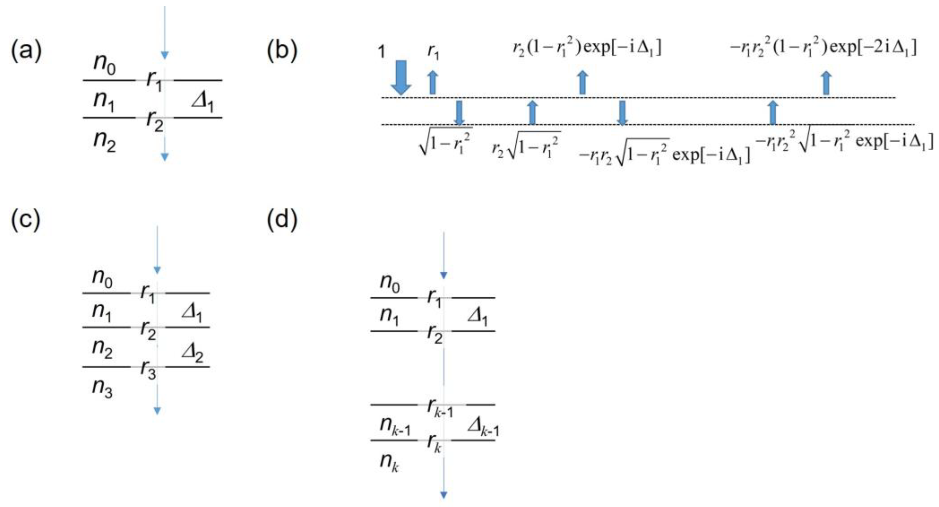
Abstract
:1. Introduction
2. Results
2.1. Multiple Reflections on a Few-Layer Structure
2.1.1. Three Layers (Two Interfaces)
- The fraction of the amplitude of the light which is reflected and transmitted at the interface between the material 0 and 1 are given by r1 and , respectively, where r1 = (n0 − n1)/(n0 + n1). Similarly, the reflection and transmission at the interface between the material 1 and 2 can be calculated. Notably, when light is penetrates from material 1 to 0, the additional phase factor, exp[−iΔ1] appears (Figure 1b), where Δ1 = 4πn1d1/λ and d1 is the thickness of layer 1.
- .
- .
2.1.2. Three Interfaces
- In a system with three interfaces (four layers), we can compare the result with the prototypical scenario of the cleaving experiment of graphene [16]. We employed Fresnel theory to understand the contrast of an atomically thin flake througha multiple reflections.
- Let us consider three materials denoted as 1, 2, and 3 with refractive indices of of n1, n2, and n3, respectively. On top of material 1, we assume the presence of air (vacuum) where the index is n0. The reflection of interfaces 0–1, 1–2, and 2–3 is represented by r1, r2, and r3, respectively. The phase shifts in materials 1 and 2 are represented by Δ1 and Δ2, respectively. The schematic configuration is depicted in Figure 1c. Next, we can determine the following values: r2 = (n1 − n2)/(n1 + n2), r3 = (n2 − n3)/(n2 + n3), Δ2 = 4πn2d2/λ, where λ represents the wavelength of light. The total reflection can be expressed as R = |r(2) exp [iε(2)]|2 where
- .
- .
2.1.3. General Case
- We can generalize the calculation of the contrast for multiple layers as follows.
- The materials 1, 2, …, k with refractive indices of n1, n2, …, nk, respectively. On top of material 1, we assume the presence of air (vacuum) with an index denoted as n0. The reflection of the interfaces 0–1, 1–2, …, (k − 1) –k is represented by r1, r2, and rk, respectively. The phase shifts in material 1, 2, …, k − 1 are represented by Δ1, Δ2, …, Δk−1, respectively. The schematic configuration is shown in Figure 1d. We can detemine the following values: rj = (nj−1 − nj)/(nj−1 + nj), Δj = 4πnjdj,/λ. The total reflection can be represented as Rk = ||2 where
- .
- .
- The wavelength-dependent contrast is represented as (Rk [n1 = 1] − Rk[n1 = nflake])/Rk [n1 = 1]. This formula is used to understand the experiment of Cr2Ge2Te6/NiO (refer to Section 3.1).
2.2. Experiment
2.2.1. Method
2.2.2. Result
3. Discussion
3.1. Reflection Calculation on Cr2Ge2Te6/NiO Case
3.2. Comparison with the Cr2Ge2Te6/NiO Sample
3.3. Structural and Morphological Properties
3.4. Comparison with Reported Density Functional
4. Conclusions
Supplementary Materials
Author Contributions
Funding
Data Availability Statement
Conflicts of Interest
References
- Novoselov, K.S.; Geim, A.K.; Morozov, S.V.; Jiang, D.; Katsnelson, M.I.; Grigorieva, I.V.; Dubonos, S.V.; Firsov, A.A. Two-dimensional gas of massless Dirac fermions in graphene. Nature 2005, 438, 197. [Google Scholar] [CrossRef] [PubMed] [Green Version]
- Zhang, Y.; Tan, Y.W.; Stormer, H.L.; Kim, P. Experimental observation of the quantum Hall effect and Berry’s phase in graphene. Nature 2005, 438, 201. [Google Scholar] [CrossRef] [PubMed] [Green Version]
- Ajayan, P.; Kim, P.; Banerjee, K. Two-dimensional van der Waals materials. Phys. Today 2016, 69, 38. [Google Scholar] [CrossRef]
- Gong, C.; Zhang, X. Two-dimensional magnetic crystals and emergent heterostructure devices. Science 2019, 363, eaav4450. [Google Scholar] [CrossRef] [PubMed]
- Gong, C.; Li, L.; Li, Z.; Ji, H.; Stern, A.; Xia, Y.; Cao, T.; Bao, W.; Wang, C.; Wang, Y.; et al. Discovery of intrinsic ferromagnetism in two-dimensional van der Waals crystals. Nature 2017, 546, 265–269. [Google Scholar] [CrossRef] [PubMed] [Green Version]
- Huang, B.; Clark, G.; Navarro-Moratalla, E.; Klein, D.R.; Cheng, R.; Seyler, K.L.; Zhong, D.; Schmidgall, E.; McGuire, M.A.; Cobden, D.H.; et al. Layer-dependent ferromagnetism in a van der Waals crystal down to the monolayer limit. Nature 2017, 546, 270. [Google Scholar] [CrossRef] [PubMed] [Green Version]
- Deng, Y.; Yu, Y.; Song, Y.; Zhang, J.; Wang, N.Z.; Sun, Z.; Yi, Y.; Wu, Y.Z.; Wu, S.; Zhu, J.; et al. Gate-tunable room-temperature ferromagnetism in two-dimensional Fe3GeTe2. Nature 2018, 563, 94. [Google Scholar] [CrossRef] [Green Version]
- Lee, J.-U.; Lee, S.; Ryoo, J.H.; Kang, S.; Kim, T.Y.; Kim, P.; Park, C.-H.; Park, J.-G.; Cheong, H. Ising-Type Magnetic Ordering in Atomically Thin FePS3. Nano Lett. 2016, 16, 7433–7438. [Google Scholar] [CrossRef] [Green Version]
- Long, G.; Zhang, T.; Cai, X.; Hu, J.; Cho, C.; Xu, S.; Shen, J.; Wu, Z.; Han, T.; Lin, J.; et al. Isolation and Characterization of Few-Layer Manganese Thiophosphite. ACS Nano 2017, 11, 11330. [Google Scholar] [CrossRef] [PubMed] [Green Version]
- Idzuchi, H.; Pientka, F.; Huang, K.-F.; Harada, K.; Gül, Ö.; Shin, Y.J.; Nguyen, L.T.; Jo, N.H.; Shindo, D.; Cava, R.J.; et al. Unconventional supercurrent phase in Ising superconductor Josephson junction with atomically thin magnetic insulator. Nat. Commun. 2021, 12, 5332. [Google Scholar] [CrossRef] [PubMed]
- Ding, B.; Dong, B.; Li, Y.; Chen, M.; Li, X.; Huang, J.; Wang, H.; Zhao, X.; Li, Y.; Li, D.; et al. Electric-field control of magnetism in a few-layered van der Waals ferromagnetic semiconductor. Nat. Nanotechnol. 2018, 13, 554–559. [Google Scholar]
- Sun, Y.; Xiao, R.C.; Lin, G.T.; Zhang, R.R.; Ling, L.S.; Ma, Z.W.; Luo, X.; Lu, W.J.; Sun, Y.P.; Sheng, Z.G. Effects of hydrostatic pressure on spin-lattice coupling in two-dimensional ferromagnetic Cr2Ge2Te6. Appl. Phys. Lett. 2018, 112, 072409. [Google Scholar] [CrossRef]
- Idzuchi, H.; Allcca, A.E.L.; Pan, X.C.; Tanigaki, K.; Chen, Y.P. Increased Curie temperature and enhanced perpendicular magneto anisotropy of Cr2Ge2Te6/NiO heterostructures. Appl. Phys. Lett. 2019, 115, 232403. [Google Scholar] [CrossRef] [Green Version]
- Idzuchi, H.; Allcca, A.E.L.; Lu, A.K.A.; Saito, M.; Houssa, M.; Meng, R.; Inoue, K.; Pan, X.-C.; Tanigaki, K.; Ikuhara, Y.; et al. Enhanced ferromagnetism in artificially stretched lattice in quasi two-dimensional Cr2Ge2Te6. arXiv 2023, arXiv:2306.08962v1. [Google Scholar]
- Anders, H. Thin Films in Optics; Focal: London, UK, 1967; Pt. 1; pp. 47–48. [Google Scholar]
- Blake, P.; Hill, E.W.; Neto, A.H.C.; Novoselov, K.S.; Jiang, D.; Yang, R.; Booth, T.J.; Geim, A.K. Making graphene visible. Appl. Phys. Lett. 2007, 91, 063124. [Google Scholar] [CrossRef] [Green Version]
- Human Vision and Color Perception. Available online: https://www.olympus-lifescience.com/en/microscope-resource/primer/lightandcolor/humanvisionintro/#:~:text=When%20fully%20light%2Dadapted%2C%20the,of%20the%20visible%20light%20spectrum (accessed on 12 March 2023).
- Allcca, A.E.L.; Idzuch, H.; Pan, X.C.; Tanigaki, K.; Chen, Y.P. Modified magnetism in heterostructures of Cr2Ge2Te6 and oxides. AIP Adv. 2023, 13, 015031. [Google Scholar] [CrossRef]
- Standard Operating Procedures of Tools in Quattrone Nanofabrication Facility. Available online: https://www.seas.upenn.edu/~nanosop/documents/Session1A_UPenn_WVASE_Feb_2014.pdf (accessed on 12 March 2023).
- Castellanos-Gomez, A.; Roldán, R.; Cappelluti, E.; Buscema, M.; Guinea, F.; van der Zant, H.S.J.; Steele, G.A. Local Strain Engineering in Atomically Thin MoS2. Nano Lett. 2013, 13, 5361. [Google Scholar] [CrossRef] [PubMed] [Green Version]
- Matuda, N.; Baba, S.; Kinbara, A. Internal stress, young’s modulus and adhesion energy of carbon films on glass substrates. Thin Solid Film. 1981, 81, 301. [Google Scholar] [CrossRef]
- Fang, Y.; Wu, S.; Zhu, Z.-Z.; Guo, G.-Y. Large magneto-optical effects and magnetic anisotropy energy in two-dimensional Cr2Ge2Te6. Phys. Rev. B 2018, 98, 125416. [Google Scholar] [CrossRef] [Green Version]


Disclaimer/Publisher’s Note: The statements, opinions and data contained in all publications are solely those of the individual author(s) and contributor(s) and not of MDPI and/or the editor(s). MDPI and/or the editor(s) disclaim responsibility for any injury to people or property resulting from any ideas, methods, instructions or products referred to in the content. |
© 2023 by the authors. Licensee MDPI, Basel, Switzerland. This article is an open access article distributed under the terms and conditions of the Creative Commons Attribution (CC BY) license (https://creativecommons.org/licenses/by/4.0/).
Share and Cite
Idzuchi, H.; Llacsahuanga Allcca, A.E.; Haglund, A.V.; Pan, X.-C.; Matsuda, T.; Tanigaki, K.; Mandrus, D.; Chen, Y.P. On the Optical Properties of Cr2Ge2Te6 and Its Heterostructure. Condens. Matter 2023, 8, 59. https://doi.org/10.3390/condmat8030059
Idzuchi H, Llacsahuanga Allcca AE, Haglund AV, Pan X-C, Matsuda T, Tanigaki K, Mandrus D, Chen YP. On the Optical Properties of Cr2Ge2Te6 and Its Heterostructure. Condensed Matter. 2023; 8(3):59. https://doi.org/10.3390/condmat8030059
Chicago/Turabian StyleIdzuchi, Hiroshi, Andres E. Llacsahuanga Allcca, Amanda Victo Haglund, Xing-Chen Pan, Takuya Matsuda, Katsumi Tanigaki, David Mandrus, and Yong P. Chen. 2023. "On the Optical Properties of Cr2Ge2Te6 and Its Heterostructure" Condensed Matter 8, no. 3: 59. https://doi.org/10.3390/condmat8030059