Figure 1.
AES state matrices.
Figure 1.
AES state matrices.
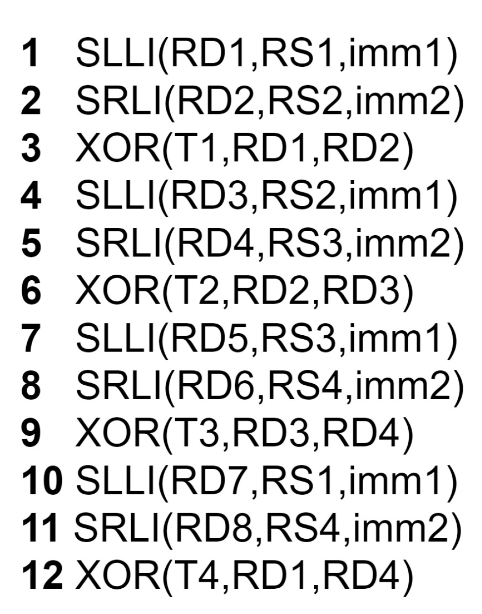
Figure 2.
AES-128 round state matrix calculation.
Figure 2.
AES-128 round state matrix calculation.
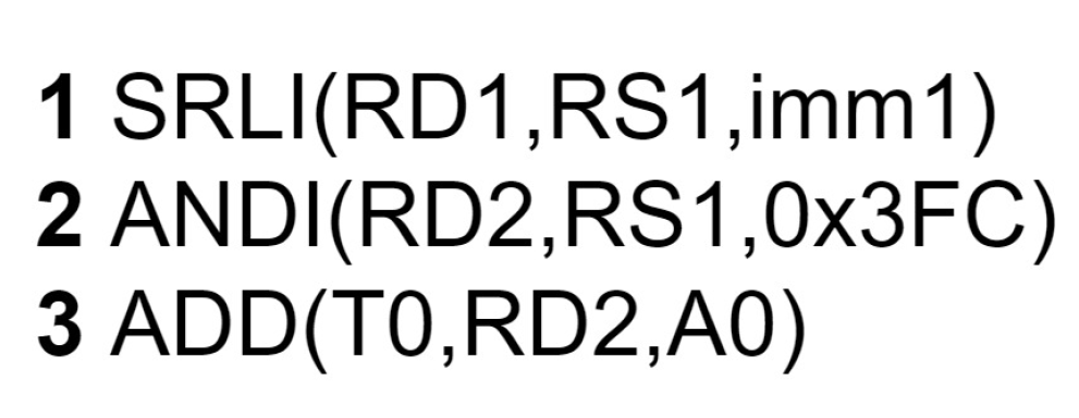
Figure 4.
Memory address calculation for 8 × 8 SBOX table.
Figure 4.
Memory address calculation for 8 × 8 SBOX table.
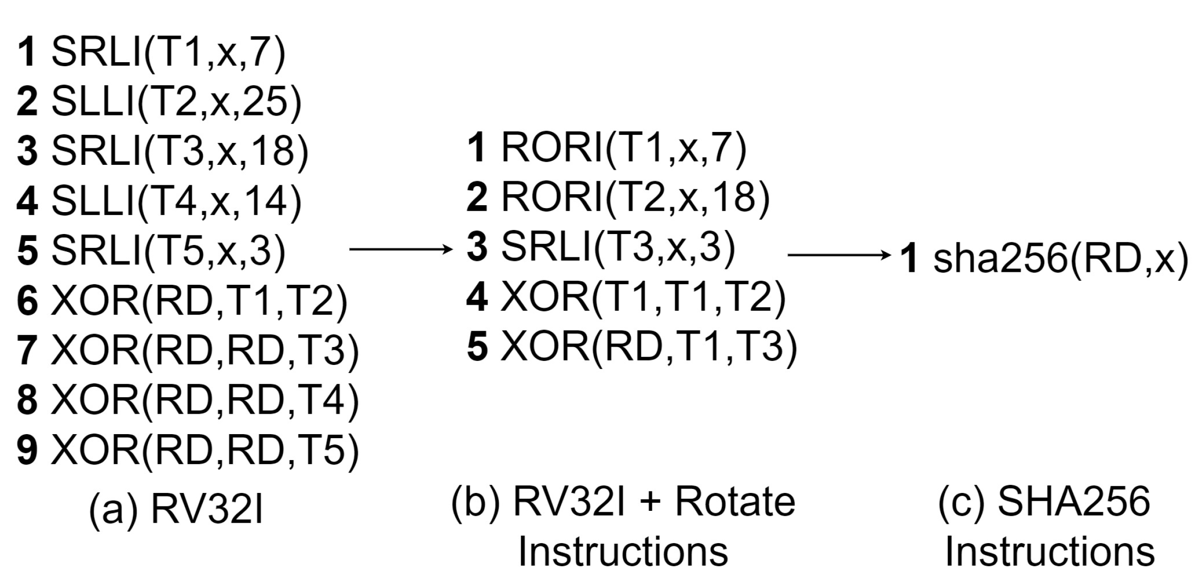
Figure 5.
Assembly code for 128-bit rotation using rv32i.
Figure 5.
Assembly code for 128-bit rotation using rv32i.
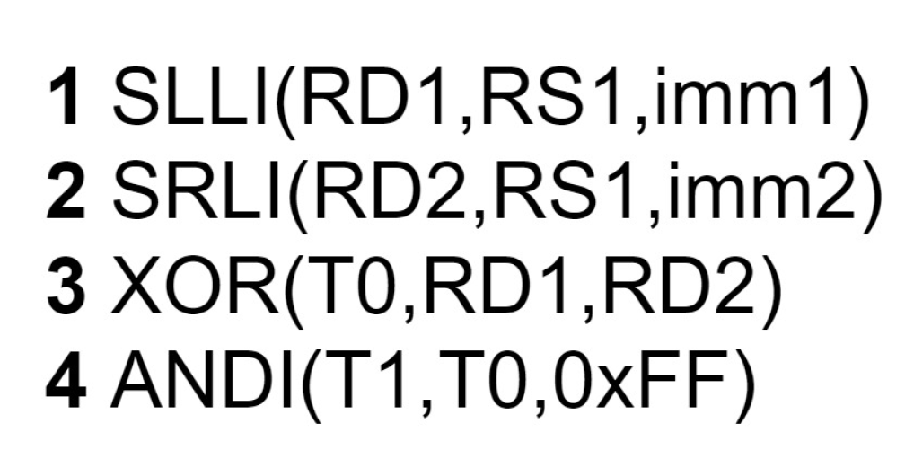
Figure 6.
Assembly code for 8-bit rotation using rv32i.
Figure 6.
Assembly code for 8-bit rotation using rv32i.
Figure 7.
Memory address calculation for 8 × 32 SBOX table using rv32i.
Figure 7.
Memory address calculation for 8 × 32 SBOX table using rv32i.
Figure 8.
SHA-256 0 function software implementation.
Figure 8.
SHA-256 0 function software implementation.
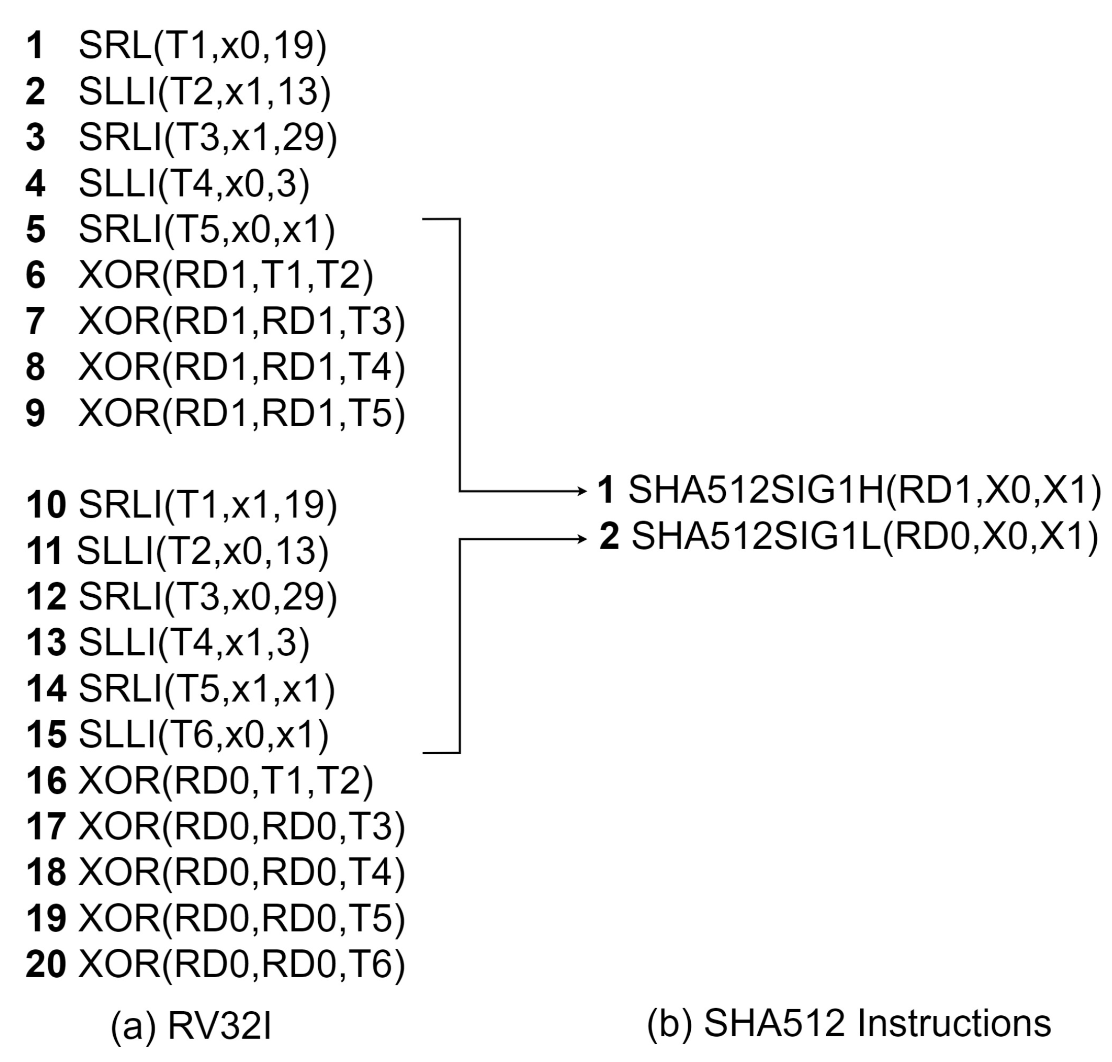
Figure 9.
SHA-512 1 function software implementation.
Figure 9.
SHA-512 1 function software implementation.
Figure 10.
Single-bit permutation using rv32i.
Figure 10.
Single-bit permutation using rv32i.
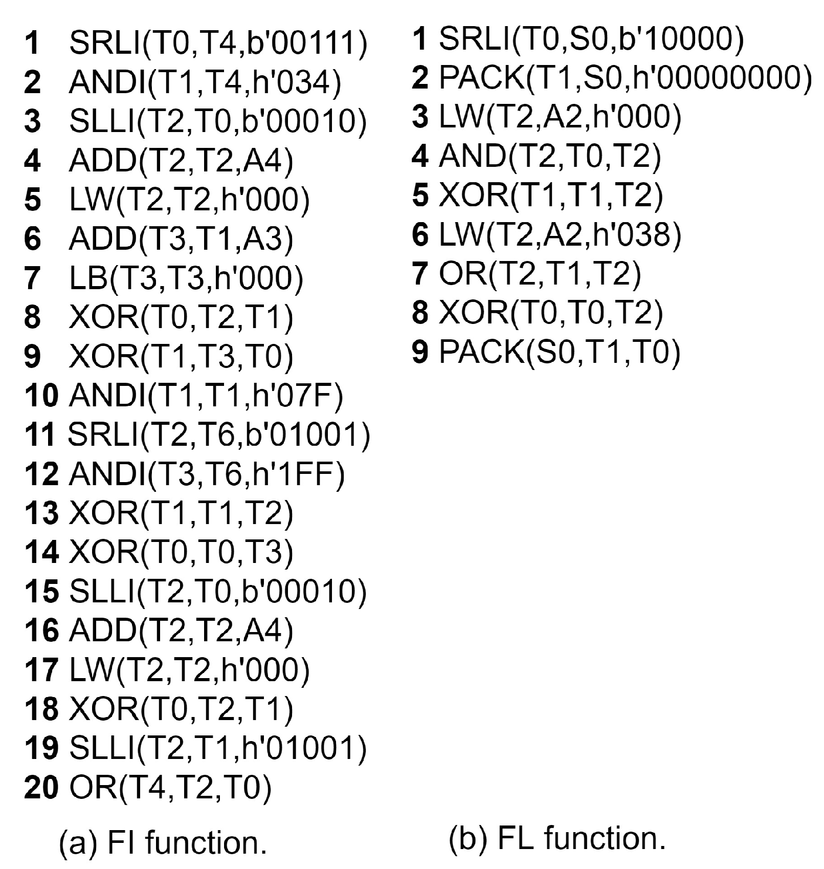
Figure 11.
MISTY1 FI and FL functions using the PACK instruction.
Figure 11.
MISTY1 FI and FL functions using the PACK instruction.
Figure 12.
HIGHT encryption.
Figure 12.
HIGHT encryption.
Figure 13.
PRESENT “sBoxLayer” using crossbar permutation instructions.
Figure 13.
PRESENT “sBoxLayer” using crossbar permutation instructions.
Figure 14.
PRESENT “pLayer” using generalized shuffle instructions.
Figure 14.
PRESENT “pLayer” using generalized shuffle instructions.
Figure 15.
Hardware architecture of re-positioning instructions.
Figure 15.
Hardware architecture of re-positioning instructions.
Figure 16.
The 4-bit matrix multiplication in GF(2).
Figure 16.
The 4-bit matrix multiplication in GF(2).
Figure 17.
Carry-less multiplication.
Figure 17.
Carry-less multiplication.
Figure 18.
Hardware architecture of carry-less multiply instructions.
Figure 18.
Hardware architecture of carry-less multiply instructions.
Figure 19.
Hardware implementation of hash instructions.
Figure 19.
Hardware implementation of hash instructions.
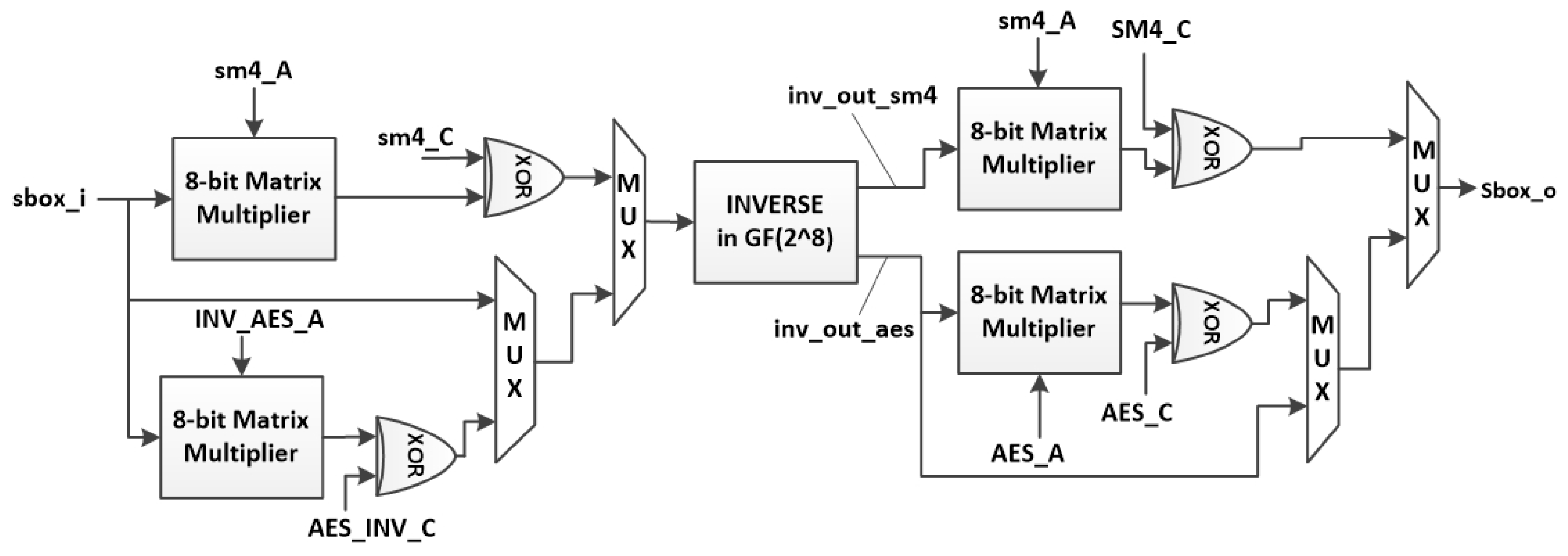
Figure 20.
Hardware implementation of AES and SM4 instructions.
Figure 20.
Hardware implementation of AES and SM4 instructions.
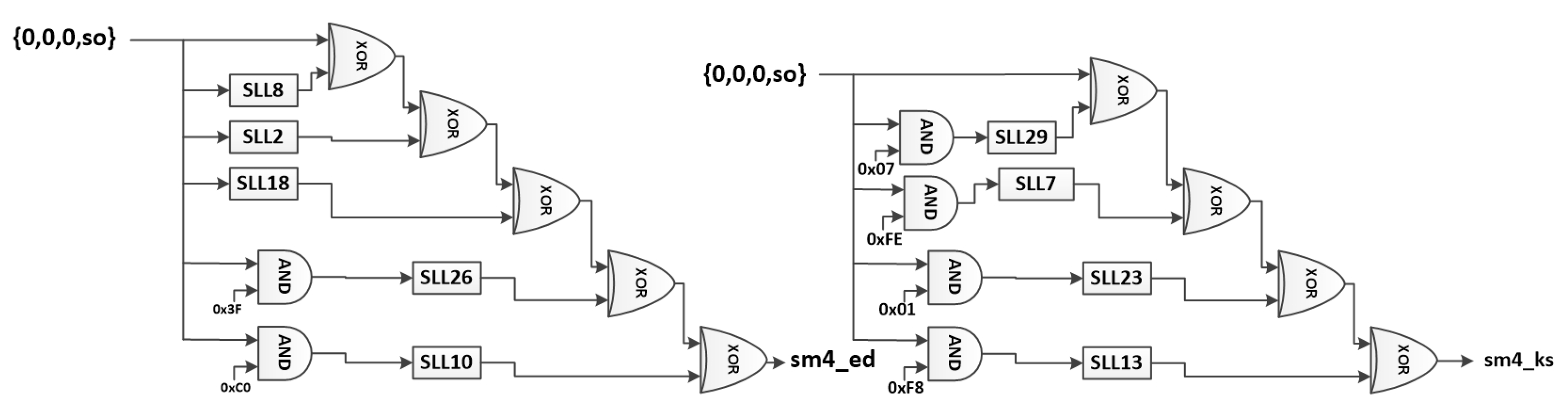
Figure 21.
SM4 operations module.
Figure 21.
SM4 operations module.
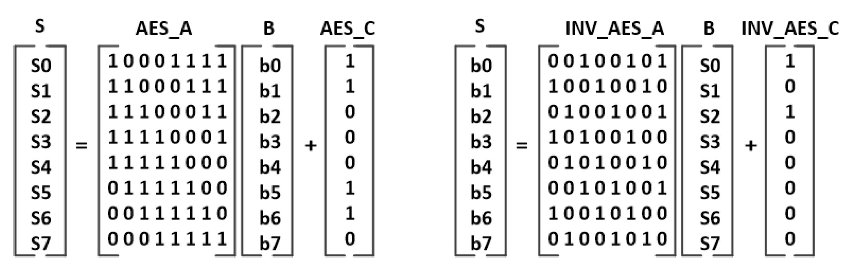
Figure 22.
AES forward and inverse SBOX affine transformations.
Figure 22.
AES forward and inverse SBOX affine transformations.
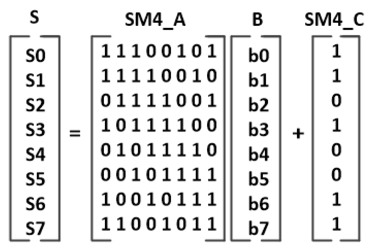
Figure 23.
SM4 affine transformation.
Figure 23.
SM4 affine transformation.
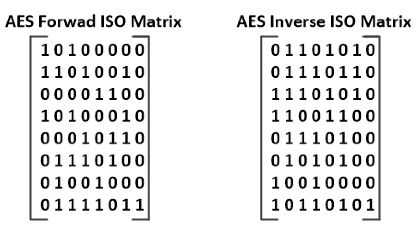
Figure 24.
AES binary matrices for forward and inverse ISO transformation.
Figure 24.
AES binary matrices for forward and inverse ISO transformation.
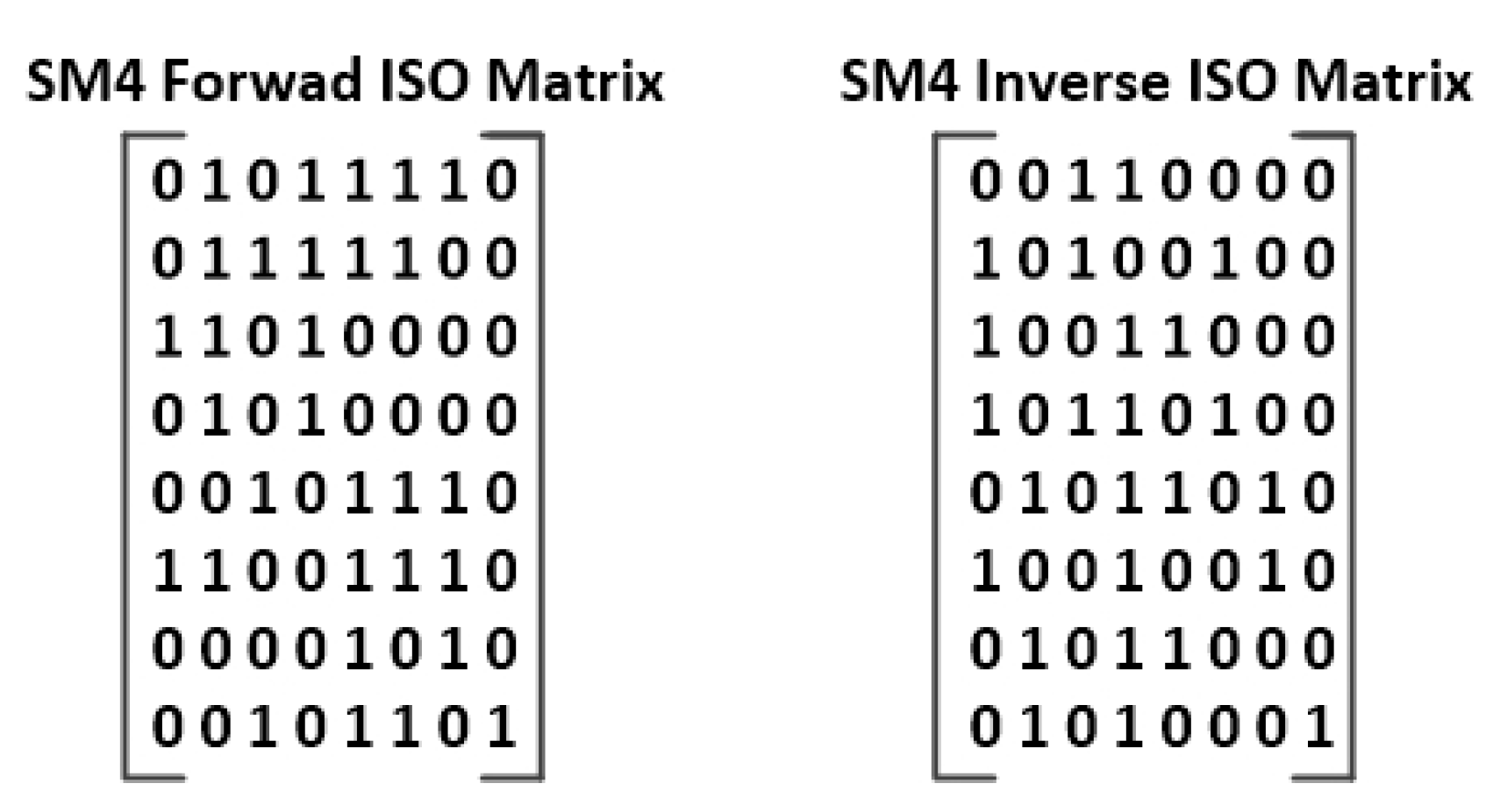
Figure 25.
SM4 binary matrices for forward and inverse ISO transformation.
Figure 25.
SM4 binary matrices for forward and inverse ISO transformation.
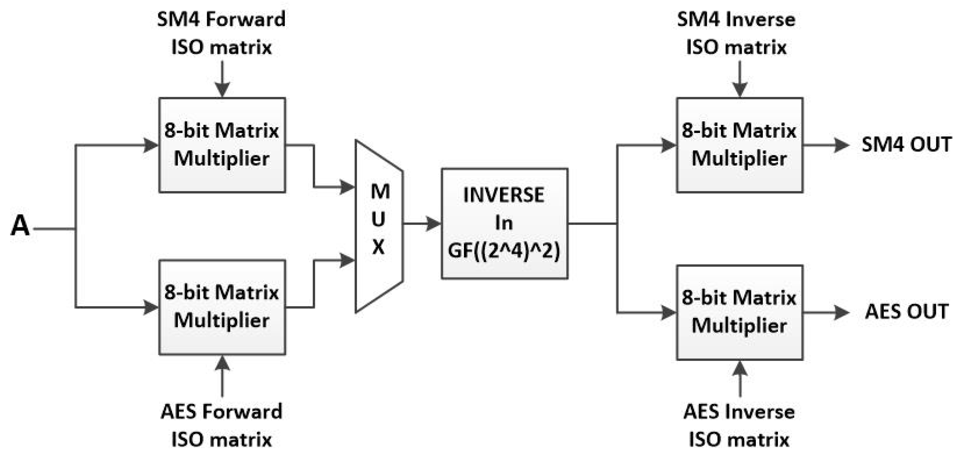
Figure 27.
Hardware architecture of “inverse in ” module.
Figure 27.
Hardware architecture of “inverse in ” module.
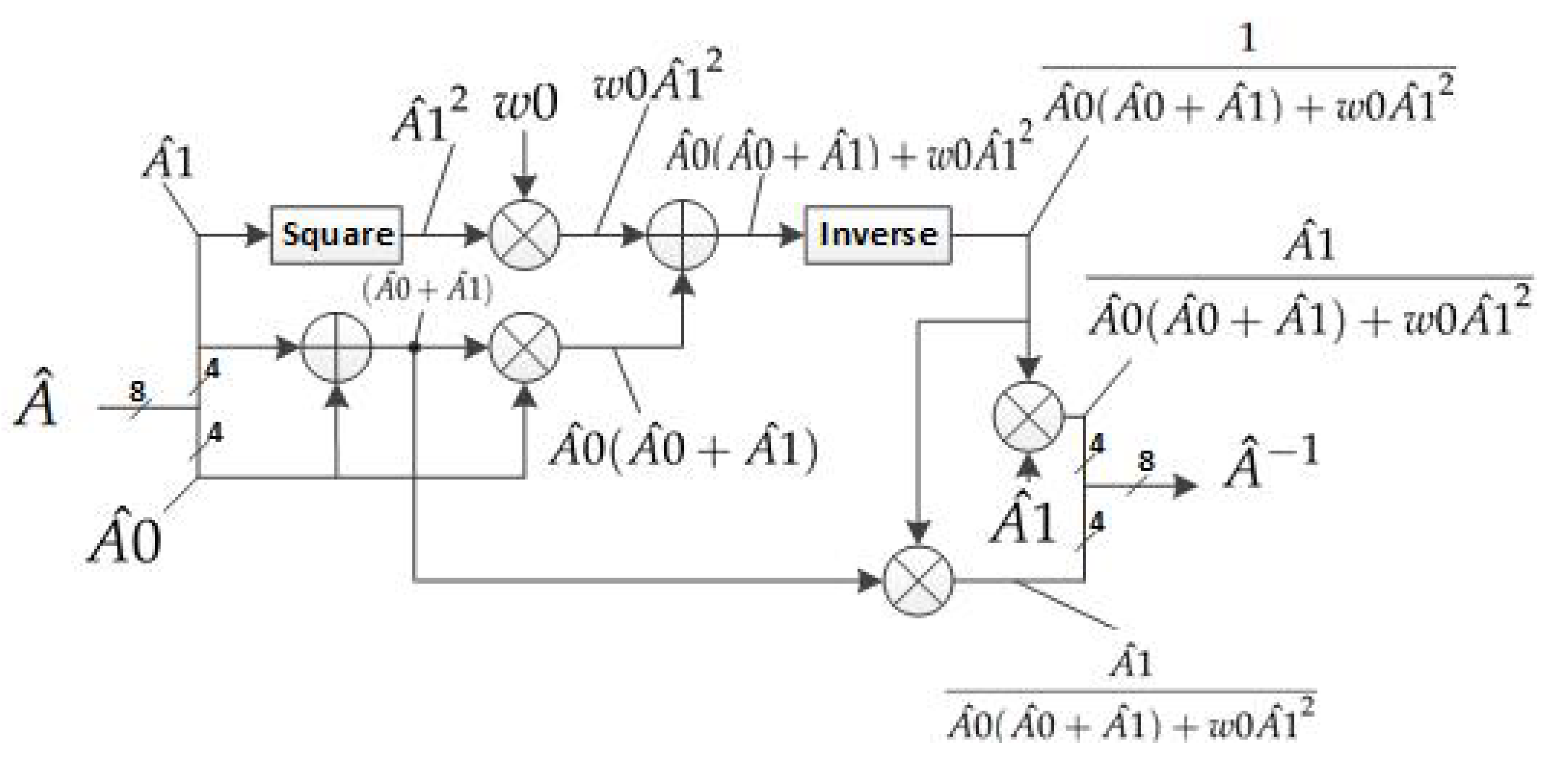
Figure 28.
Hardware architecture of “inverse in GF(” module.
Figure 28.
Hardware architecture of “inverse in GF(” module.
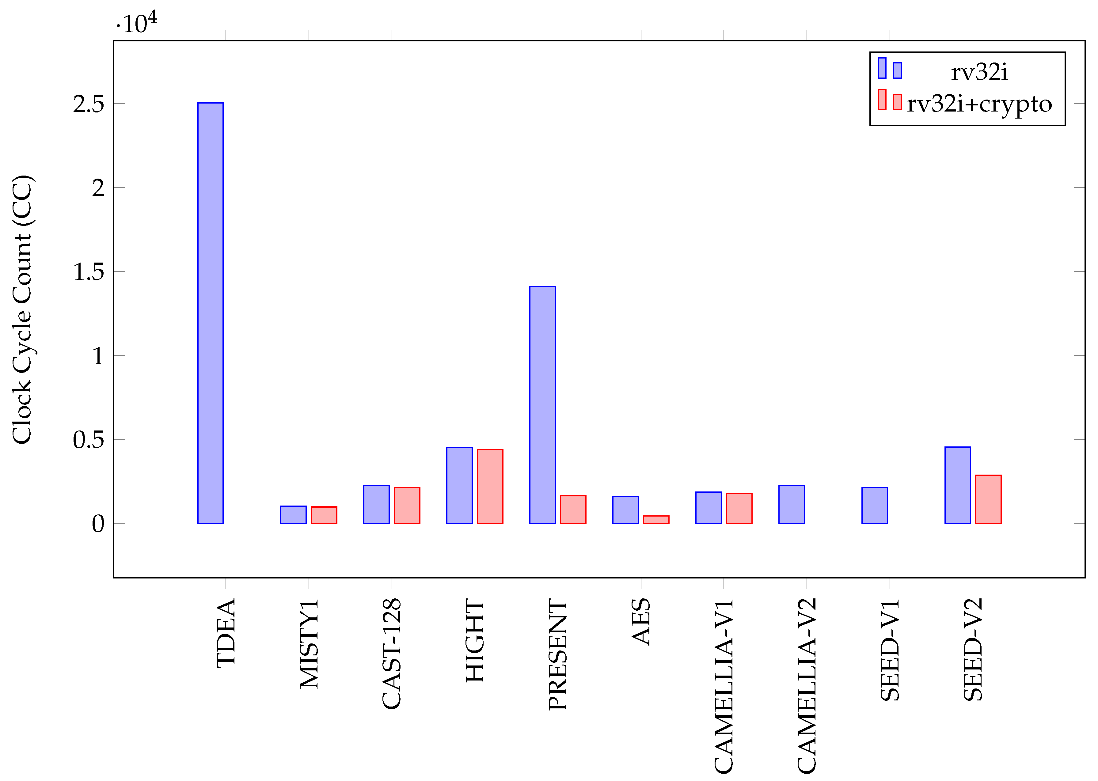
Figure 29.
Clock cycle count of block ciphers.
Figure 29.
Clock cycle count of block ciphers.
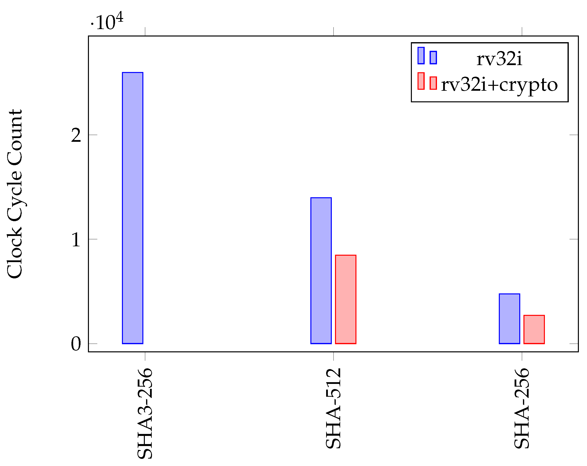
Figure 30.
Clock cycle count of hash functions.
Figure 30.
Clock cycle count of hash functions.
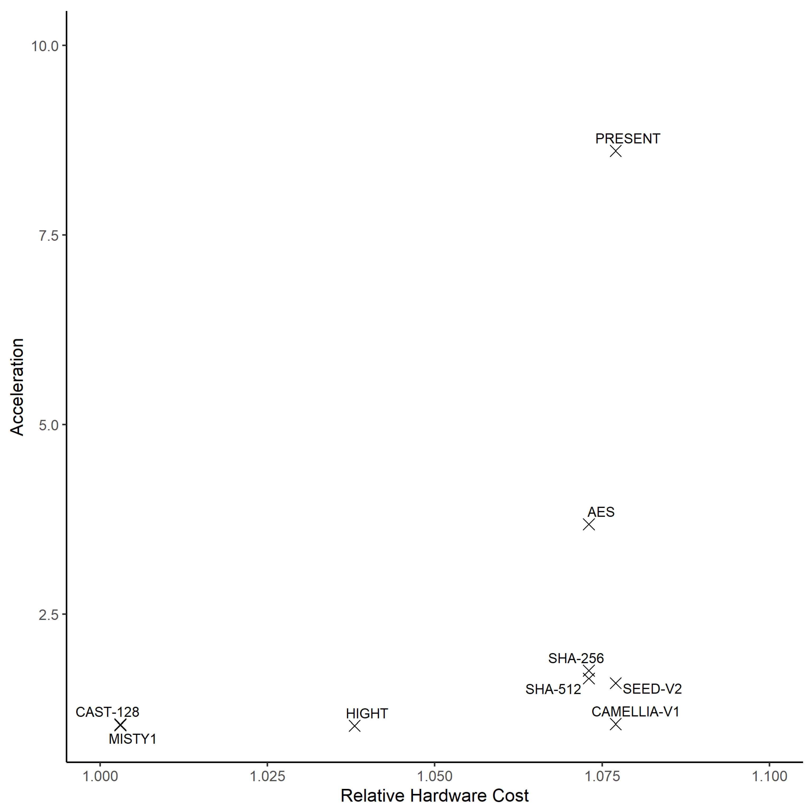
Figure 31.
Acceleration vs. hardware cost of implementation of crypto implementations.
Figure 31.
Acceleration vs. hardware cost of implementation of crypto implementations.
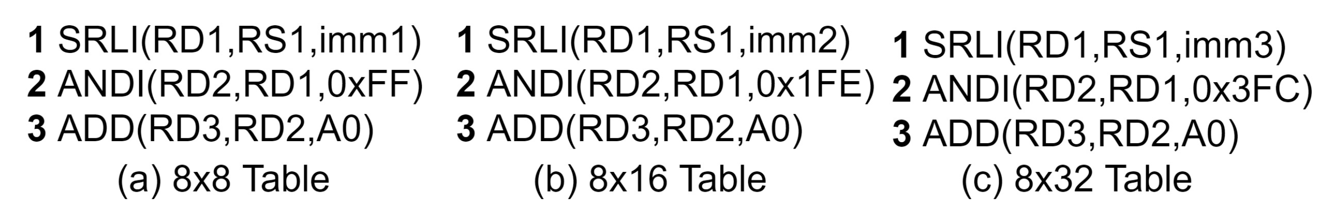
Figure 32.
Assembly code for address calculation of 8-bit input SBOX tables.
Figure 32.
Assembly code for address calculation of 8-bit input SBOX tables.
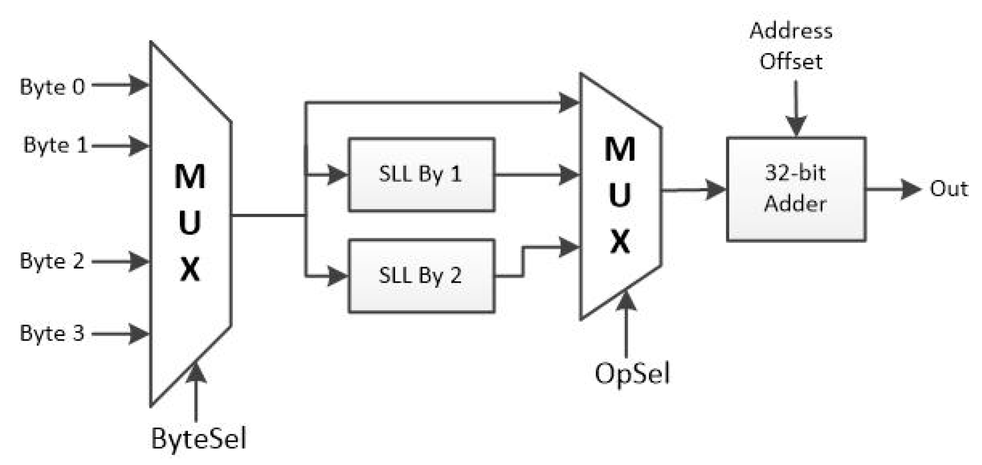
Figure 33.
Hardware architecture of address calculation instruction.
Figure 33.
Hardware architecture of address calculation instruction.
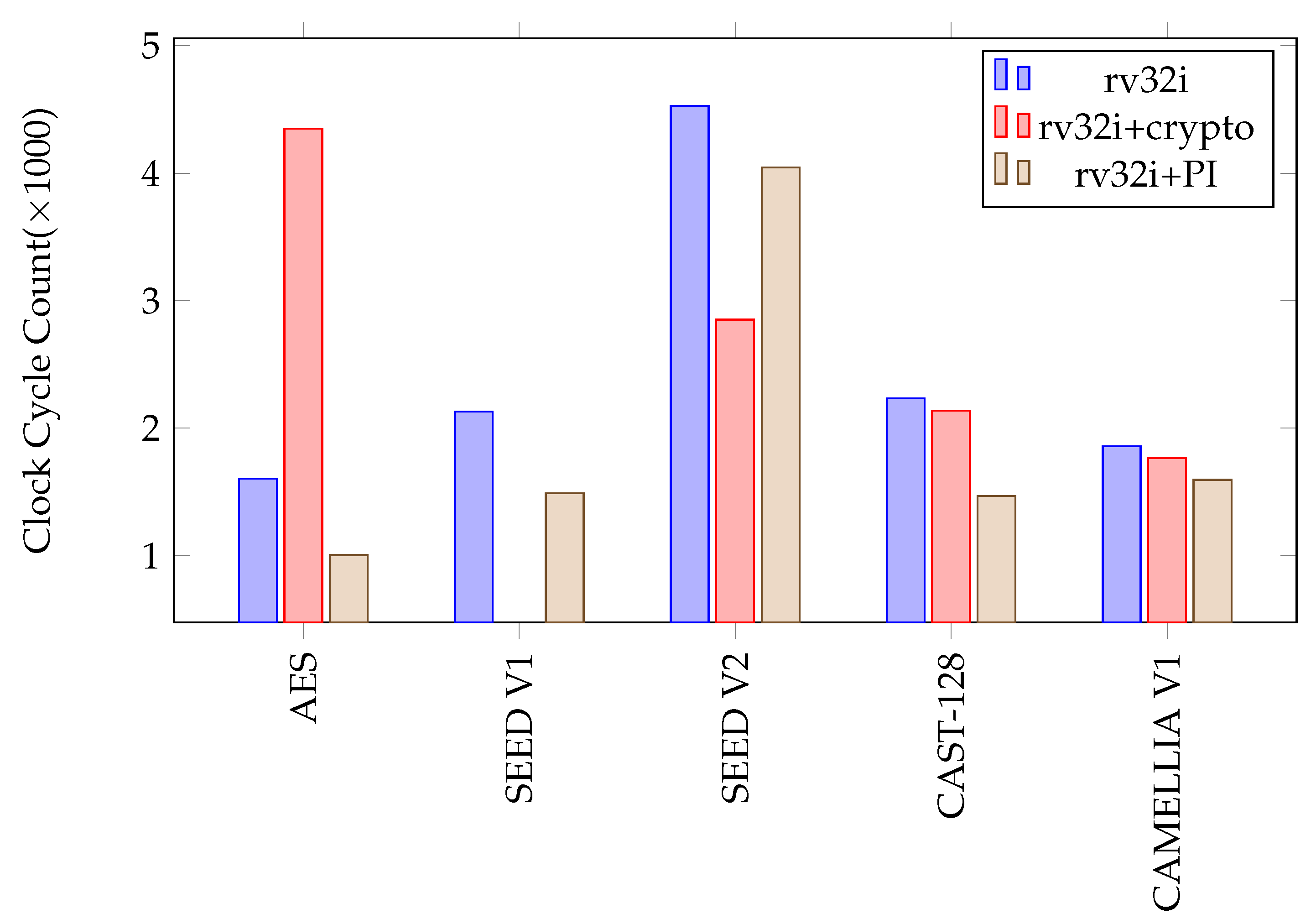
Figure 34.
Clock cycle count comparison.
Figure 34.
Clock cycle count comparison.
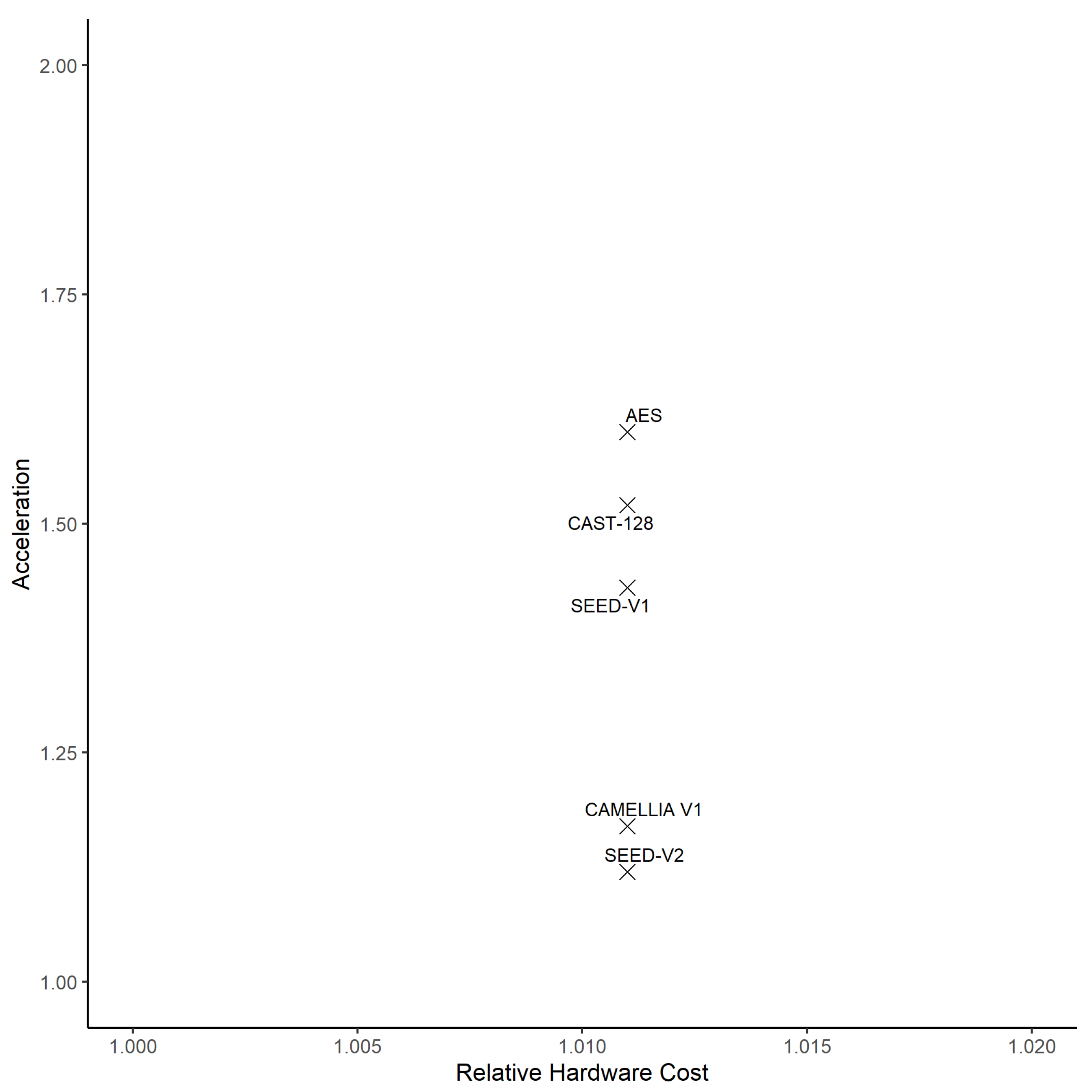
Figure 35.
Acceleration vs. hardware cost of crypto implementations with new address calculation instruction.
Figure 35.
Acceleration vs. hardware cost of crypto implementations with new address calculation instruction.
Table 1.
Symmetric block ciphers.
Table 1.
Symmetric block ciphers.
| Cipher | Block Size (Bits) | Key Size (Bits) | Comment | Reference |
|---|
| AES | 128 | 128,192,256 | ISO/IEC 18033-3:2010, FIPS 197 | [8,32] |
| SEED | 128 | 128 | ISO/IEC 18033-3:2010 | [29,32] |
| CAMELLIA | 128 | 128,192,256 | ISO/IEC 18033-3:2010 | [28,32] |
| MISTY1 | 64 | 128 | ISO/IEC 18033-3:2010 | [24,32] |
| CAST-128 | 64 | 40 to 128 | ISO/IEC 18033-3:2010 | [25,32] |
| HIGHT | 64 | 128 | ISO/IEC 18033-3:2010 | [26,32] |
| TDEA | 64 | 112,168 | ISO/IEC 18033-3:2010 | [23,32] |
| PRESENT | 64 | 80,128 | ISO/IEC 29192-2:2019 | [27,33] |
Table 2.
Hash functions.
| Function | Output Size (Bits) | State Size (Bits) | Round # | Comment | Reference |
|---|
| SHA-256 | 256 | 256 (8 × 32) | 64 | FIPS 180-3 | [9] |
| SHA-512 | 512 | 512 (8 × 64) | 80 | FIPS 180-3 | [9] |
| SHA3-256 | 256 | 1600 (5 ×5 ×64) | 24 | FIPS 202 | [30] |
Table 3.
Inverse of Elements in GF().
Table 3.
Inverse of Elements in GF().
| Element | Inverse |
|---|
| = 1 | 1 |
| = y | |
| = | |
| = | |
| = | |
| = | |
| = | |
| = | |
| = | |
| = | |
| = | |
| = | |
| = | |
| = | |
| = | y |
| = 1 | 1 |
Table 4.
Clock cycle count of 64-bit block ciphers.
Table 4.
Clock cycle count of 64-bit block ciphers.
| Algorithm | TDEA | MISTY1 | CAST-128 | HIGHT | PRESENT |
|---|
| rv32i | 25,041 | 1013 | 2237 | 4528 | 14,102 |
| rv32i+crypto | NC | 977 | 2139 | 4400 | 1641 |
| Acceleration | NC | 1.037 | 1.046 | 1.029 | 8.607 |
Table 5.
Clock cycle count of 128-bit block ciphers.
Table 5.
Clock cycle count of 128-bit block ciphers.
| Algorithm | AES | CAMELLIA V1 | CAMELLIA V2 | SEED V1 | SEED V2 |
|---|
| rv32i | 1606 | 1861 | 2258 | 2133 | 4533 |
| rv32i+crypto | 438 | 1768 | NC | NC | 2854 |
| Acceleration | 3.685 | 1.053 | NC | NC | 1.589 |
Table 6.
Clock cycle count of hash functions.
Table 6.
Clock cycle count of hash functions.
| Algorithm | SHA-256 | SHA-512 | SHA3-256 |
|---|
| rv32i | 4755 | 13975 | 25,976 |
| rv32i+crypto | 2708 | 8471 | NC |
| Acceleration | 1.756 | 1.650 | NC |
Table 7.
Clock cycle count for SEED SBOX address calculation.
Table 7.
Clock cycle count for SEED SBOX address calculation.
| Algorithm | V1 (rv32i) | V2 (rv32i) | V2 (rv32i+crypto) |
|---|
| SBOX Address Calculation | 800 | 800 | 640 |
Table 8.
Clock cycle count of CAMELLIA-128 rotate operations.
Table 8.
Clock cycle count of CAMELLIA-128 rotate operations.
| Operation | V1 (rv32i) | V2 (rv32i) | V1 (rv32i+crypto) |
|---|
| 128-bit Rotate | 132 | 132 | 132 |
| 32-bit Rotate | 12 | 12 | 4 |
| 8-bit Rotate | 0 | 396 | 0 |
| SBOX Address Calculation | 440 | 440 | 352 |
Table 9.
Clock cycle count of CAST-128 operations.
Table 9.
Clock cycle count of CAST-128 operations.
| Operation | rv32i | rv32i+crypto |
|---|
| SBOX calculation | 1152 | 1152 |
| 32-bit Rotate | 64 | 16 |
Table 10.
Clock cycle count of HIGHT operations.
Table 10.
Clock cycle count of HIGHT operations.
| Operation | rv32i | rv32i+crypto |
|---|
| 8-bit Rotation | 1408 | 1280 |
Table 11.
Clock cycle count of TDEA operations.
Table 11.
Clock cycle count of TDEA operations.
| Operation | rv32i |
|---|
| Initial Permutation | 152 |
| Inverse Initial Permutation | 254 |
| SBOX Table Read | 5424 |
| E Permutation | 2016 |
| P Permutation | 6144 |
| Permuted Choice 1 | 399 |
| Permuted Choice 2 | 9216 |
Table 12.
Clock cycle count of PRESENT operations.
Table 12.
Clock cycle count of PRESENT operations.
| Operation | rv32i | rv32i+crypto |
|---|
| pLayer | 7936 | 558 |
| sBoxLayer | 5766 | 248 |
Table 13.
Program memory requirement of 64-bit block ciphers in bytes.
Table 13.
Program memory requirement of 64-bit block ciphers in bytes.
| Algorithm | TDEA | MISTY1 | CAST-128 | HIGHT | PRESENT |
|---|
| rv32i | 6680 | 3256 | 3760 | 3028 | 1552 |
| rv32i+crypto | NC | 3132 | 3704 | 2996 | 352 |
| Reduction | NC | 1.040 | 1.015 | 1.011 | 4.409 |
Table 14.
Program memory requirement of 128-bit block ciphers in bytes.
Table 14.
Program memory requirement of 128-bit block ciphers in bytes.
| Algorithm | AES | CAMELLIA V1 | CAMELLIA V2 | SEED V1 | SEED V2 |
|---|
| rv32i | 2536 | 7448 | 9032 | 1048 | 2248 |
| rv32i+crypto | 436 | 7076 | NC | NC | 1416 |
| Reduction | 5.817 | 1.053 | NC | NC | 1.588 |
Table 15.
Program memory requirement of hash functions in bytes.
Table 15.
Program memory requirement of hash functions in bytes.
| Algorithm | SHA-256 | SHA-512 | SHA3-256 |
|---|
| rv32i | 632 | 1392 | 3996 |
| rv32i+crypto | 488 | 1088 | NC |
| Reduction | 1.295 | 1.279 | NC |
Table 16.
Static memory requirement of 64-bit block ciphers in bytes.
Table 16.
Static memory requirement of 64-bit block ciphers in bytes.
| Algorithm | TDEA | MISTY1 | CAST-128 | HIGHT | PRESENT |
|---|
| Memory | 256 | 642 | 8192 | 10 | 8 |
Table 17.
Static memory requirement of 128-bit block ciphers in bytes.
Table 17.
Static memory requirement of 128-bit block ciphers in bytes.
| Algorithm | AES | CAMELLIA V1 | CAMELLIA V2 | SEED V1 | SEED V2 |
|---|
| Memory | 1288 | 1072 | 304 | 4176 | 576 |
Table 18.
Static memory requirement of SHA algorithms in bytes.
Table 18.
Static memory requirement of SHA algorithms in bytes.
| Algorithm | SHA-256 | SHA-512 | SHA3-256 |
|---|
| Memory | 288 | 704 | 188 |
Table 19.
Area (GE) of hardware modules.
Table 19.
Area (GE) of hardware modules.
| Hardware Module | AREA (GE) |
|---|
| RISC-V Core | 19,706 |
| Bit Re-positioning Instructions | 766 |
| Carry-Less Multiply Instructions | 2248.5 |
| Crossbar Permutation Instructions | 756.5 |
| Logic With Negate Instructions | 177 |
| Packing Instructions | 52 |
| Hash Instructions | 2030.5 |
| AES and SM4 Instructions | 1437 |
Table 20.
Cryptography instruction and instruction module extension usage of crypto implementations.
Table 20.
Cryptography instruction and instruction module extension usage of crypto implementations.
| Cryptographic Algorithm | Instruction Usage | Instruction Module Extension |
|---|
| AES | aes32esmi, aes32esi | AES and SM4 |
| SEED V2 | xperm4, rori | Crossbar Permutation, Bit Re-positioning |
| CAMELLIA V1 | xperm4, rol | Crossbar Permutation, Bit Re-positioning |
| MISTY1 | pack | Packing |
| CAST-128 | pack | Packing |
| HIGHT | grev | Bit Re-positioning |
| PRESENT | xperm4, unshfli, rori | Crossbar Permutation, Bit Re-positioning |
| SHA-256 | SHA-256 Instructions | Hash |
| SHA-512 | SHA-512 Instructions | Hash |
Table 21.
Area (GE) of address calculation instruction hardware module.
Table 21.
Area (GE) of address calculation instruction hardware module.
| Hardware Module | AREA (GE) |
|---|
| Address Calculation Instruction | 220 |


