
Magnetic Semiconductors as Materials for Spintronics

Abstract
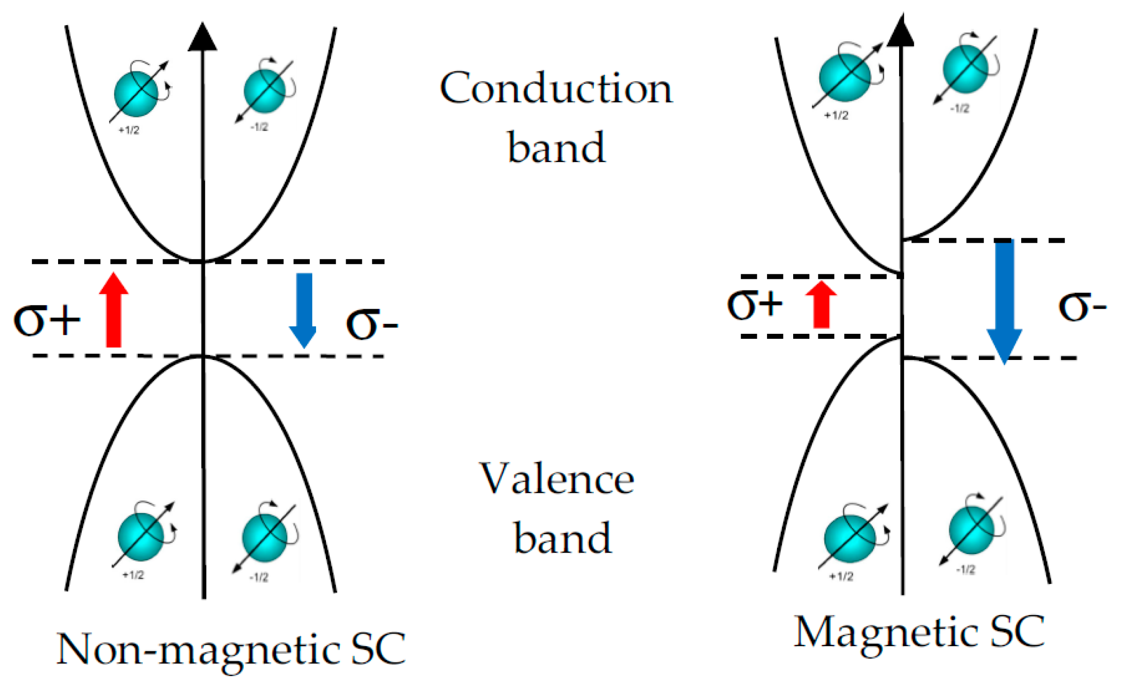
:1. Introduction
2. Functional Materials and Devices Promising for Spintronics Based on Magnetic Semiconductors
2.1. Heterostructures FM/SC
2.2. Spin Injection Maser
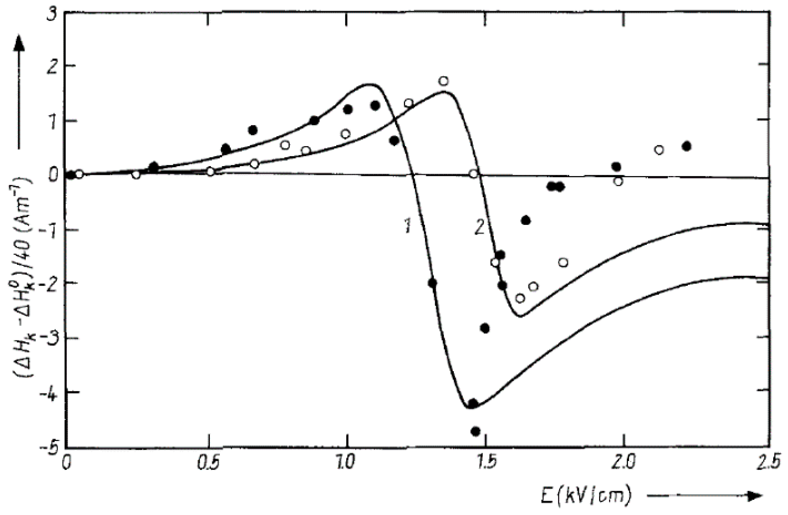
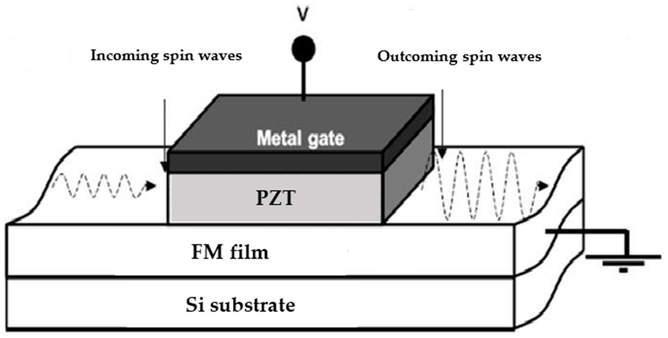
2.3. Amplification of Spin Waves by Drifting Charge Carriers
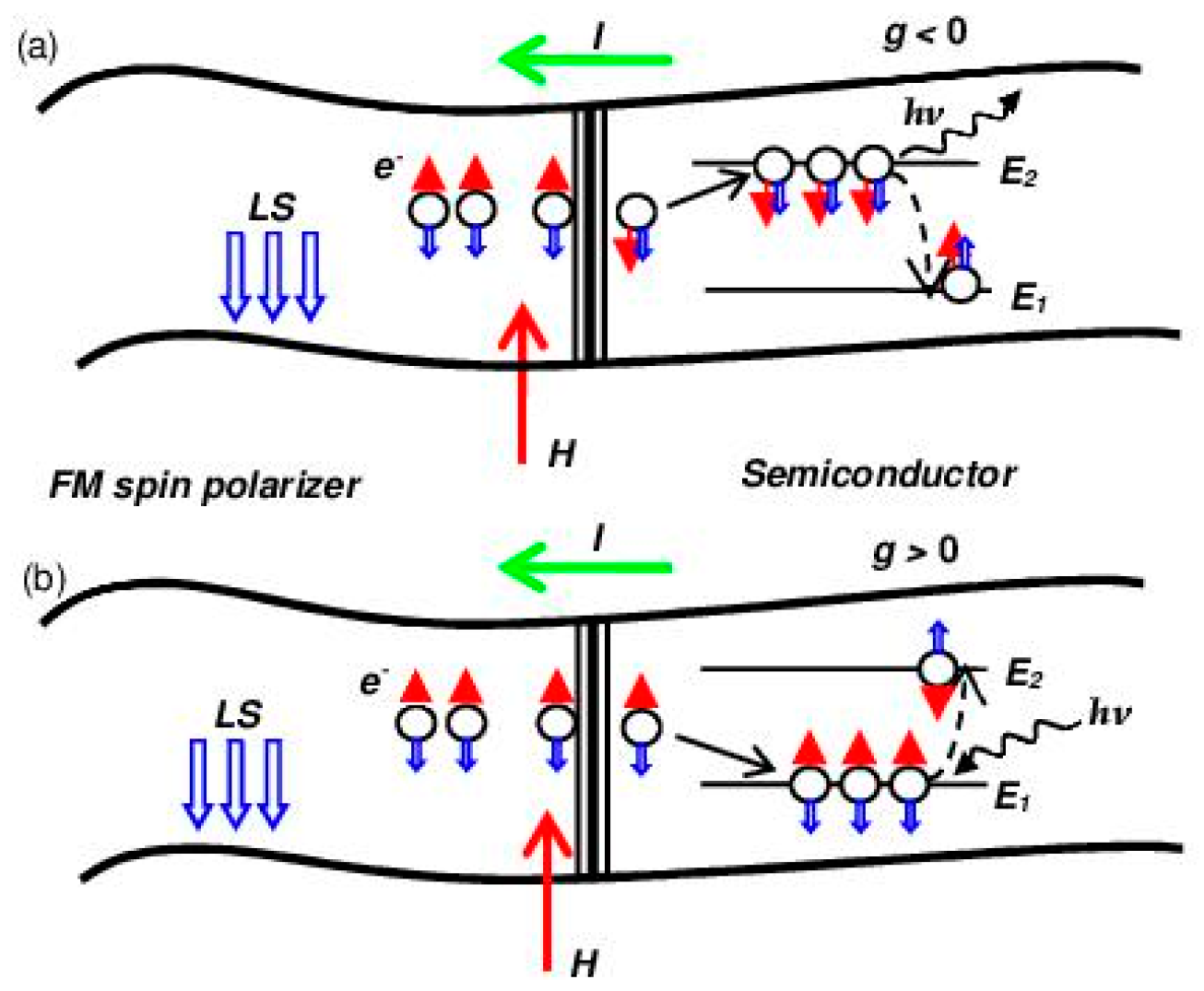
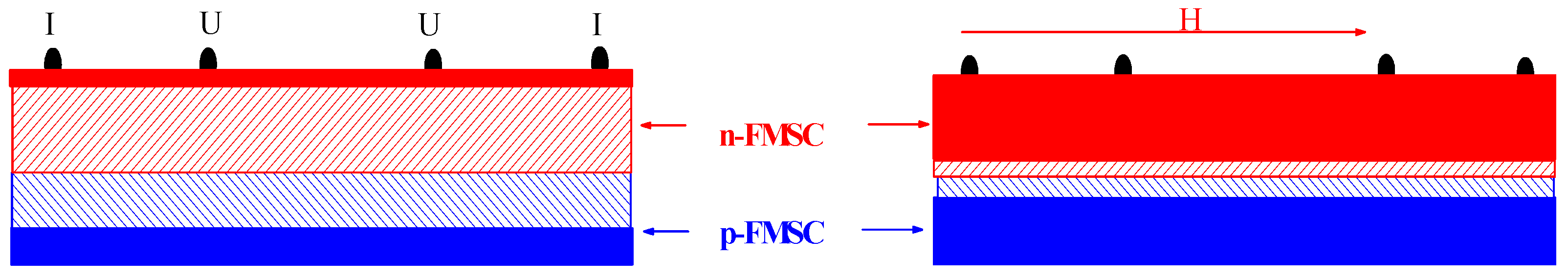
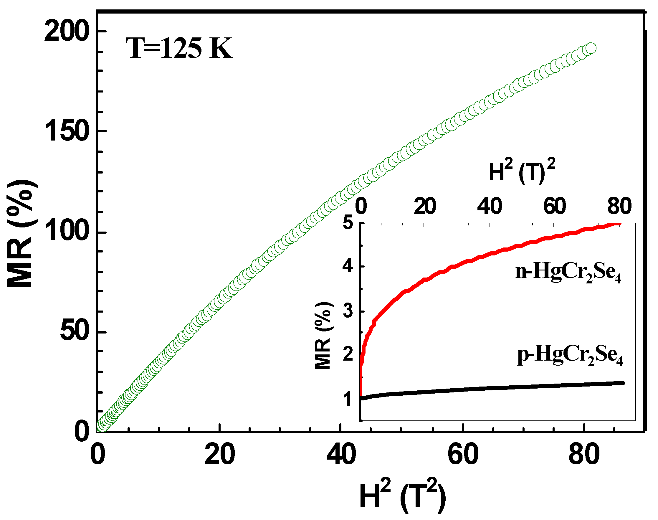
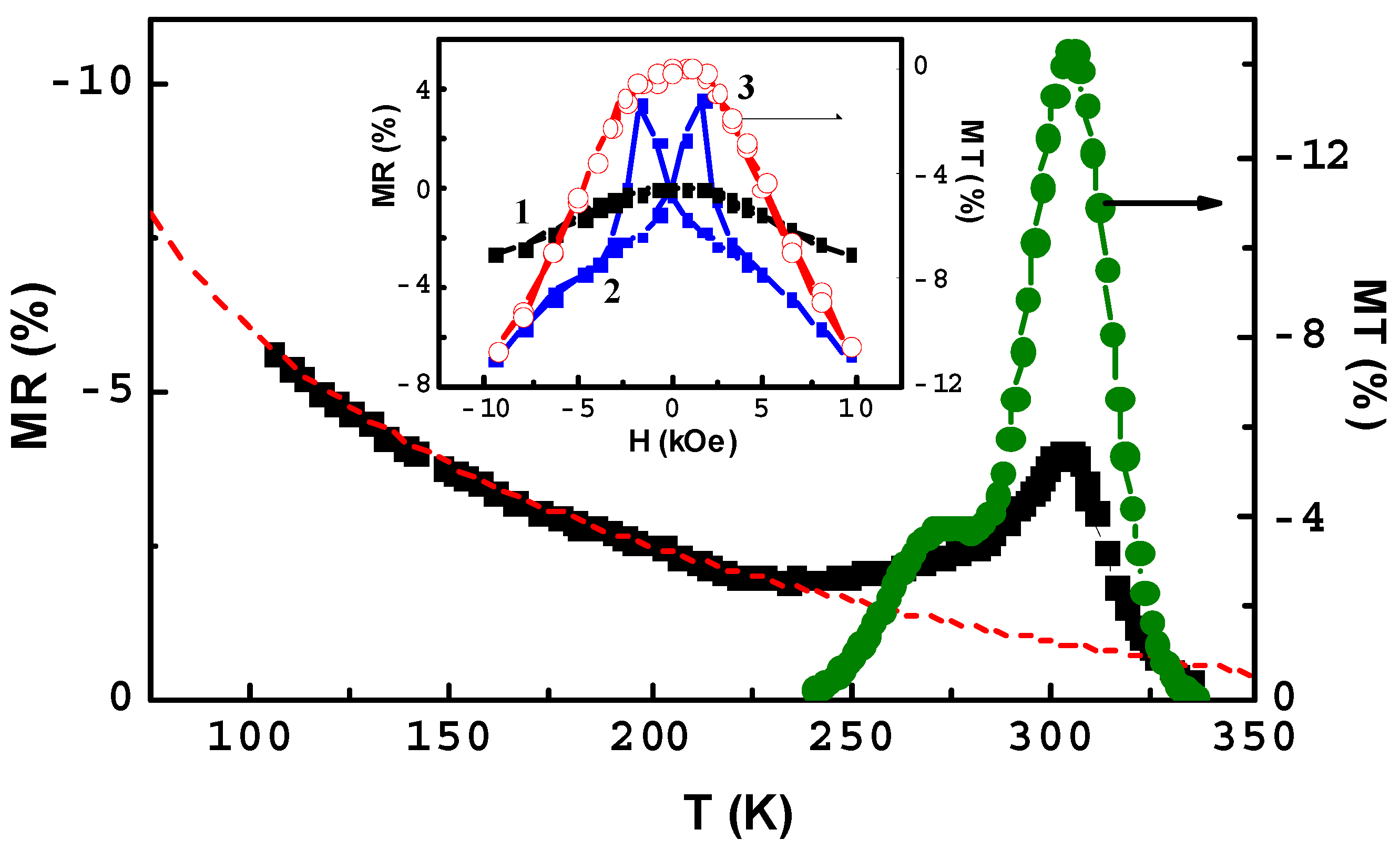
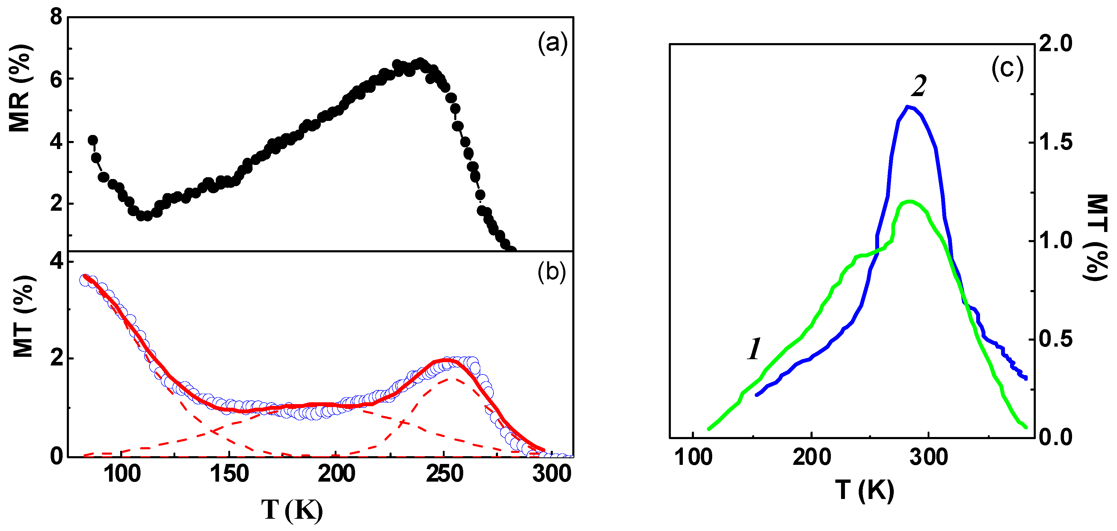
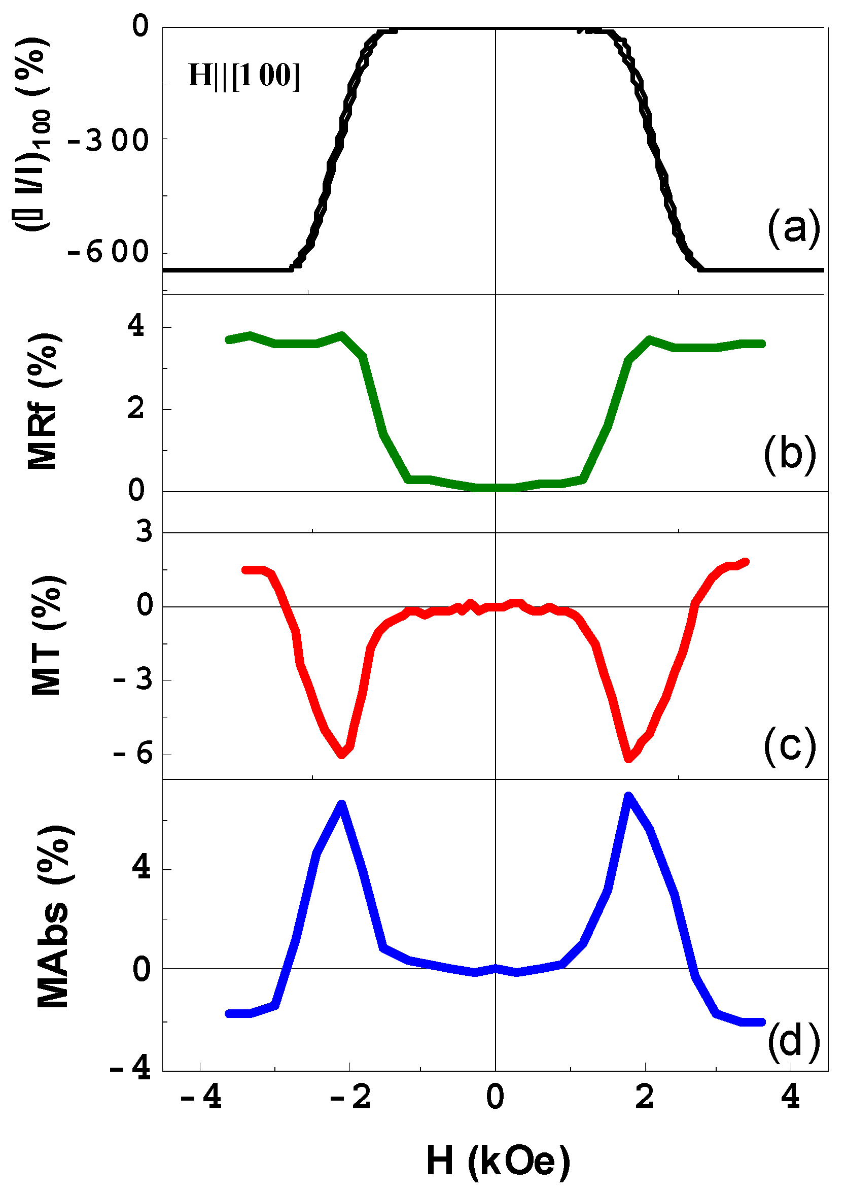
2.4. MR Structures Based on a p-n Junction in Magnetic SC
2.5. Magnetic SC with Tunnel Injection of Spin-Polarized Electrons
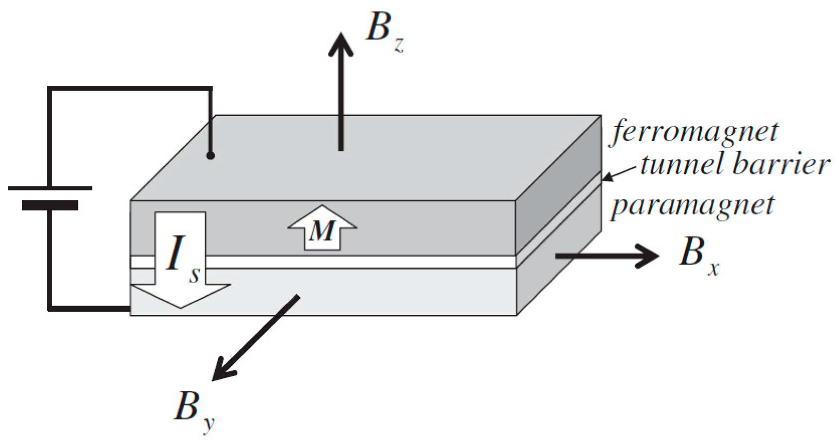
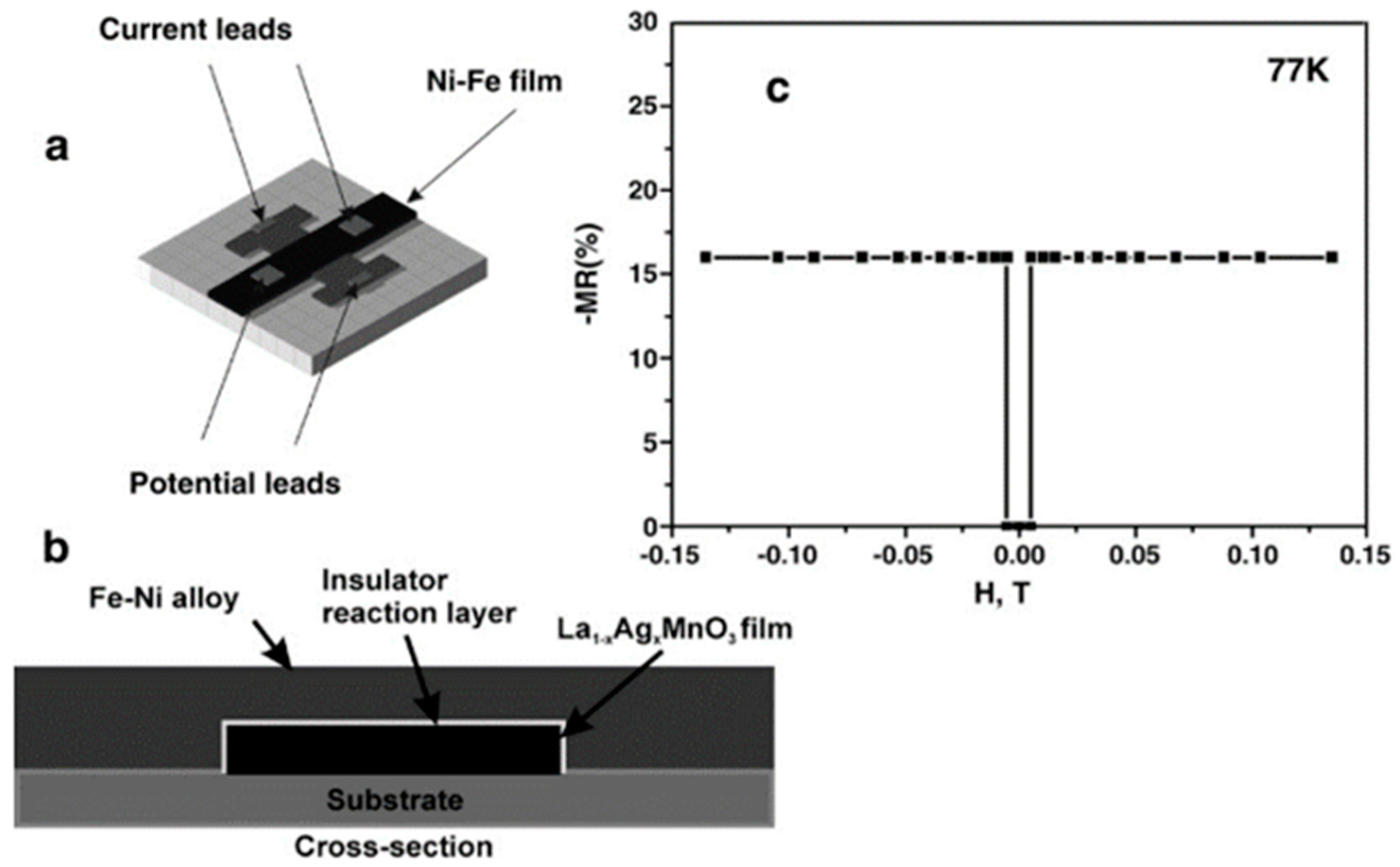
2.6. Spin Valve Structures
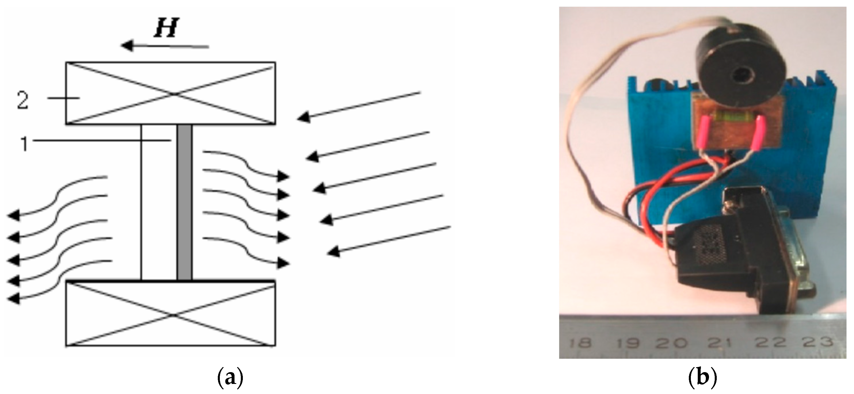
2.7. Amplitude Modulation of Light
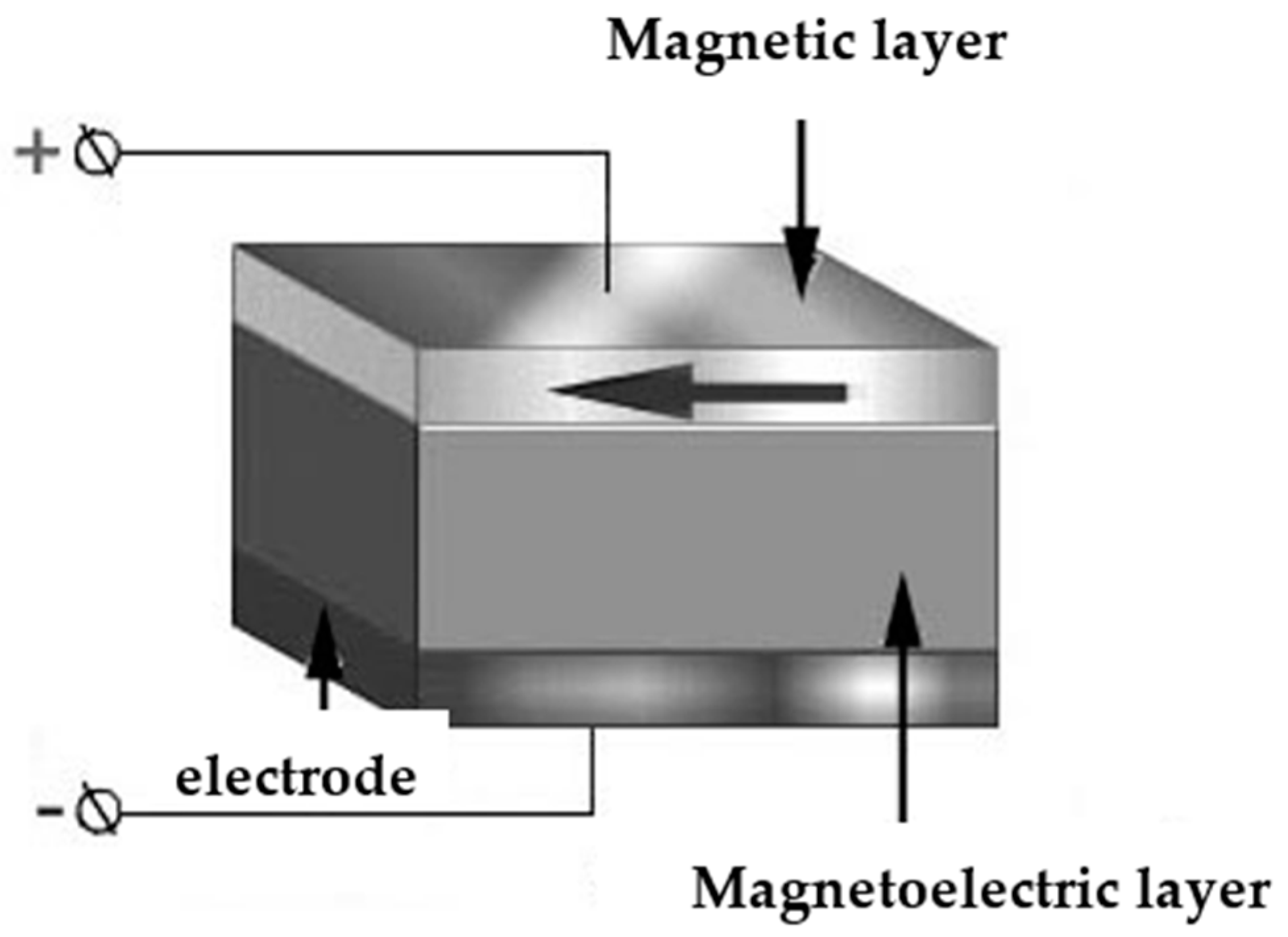
2.8. Optical Branch of Straintronics: Strain-Magnetooptics
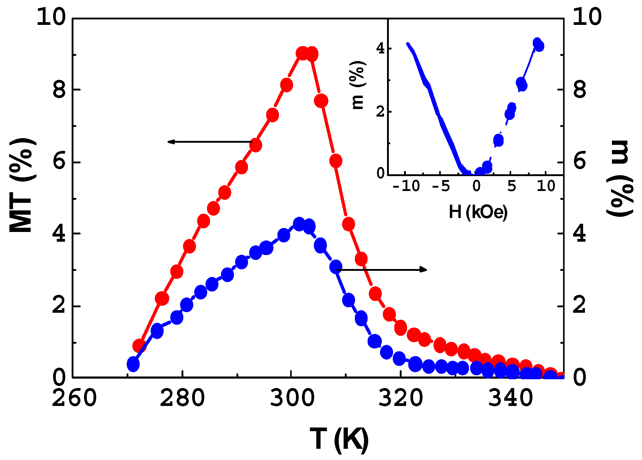
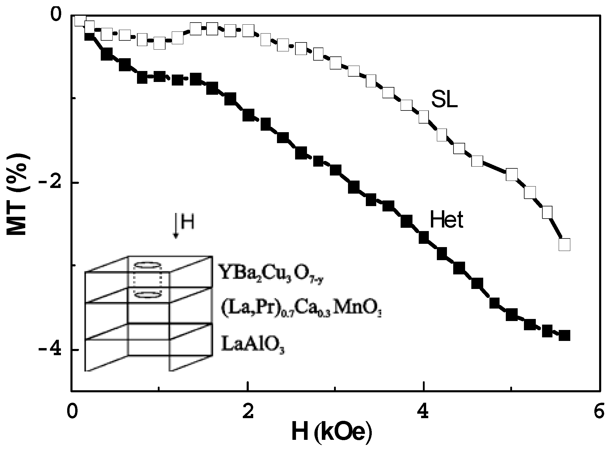
2.9. A “Magnetic Lens”—Manganite/HTSC Heterostructure
3. Nanocrystalline Magnetic Semiconductors—New Functional Materials for Spintronics
3.1. High-Density Magneto-Optical Nanoceramics
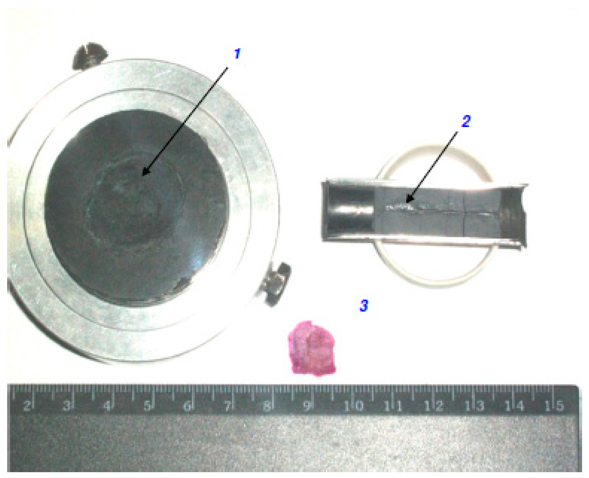
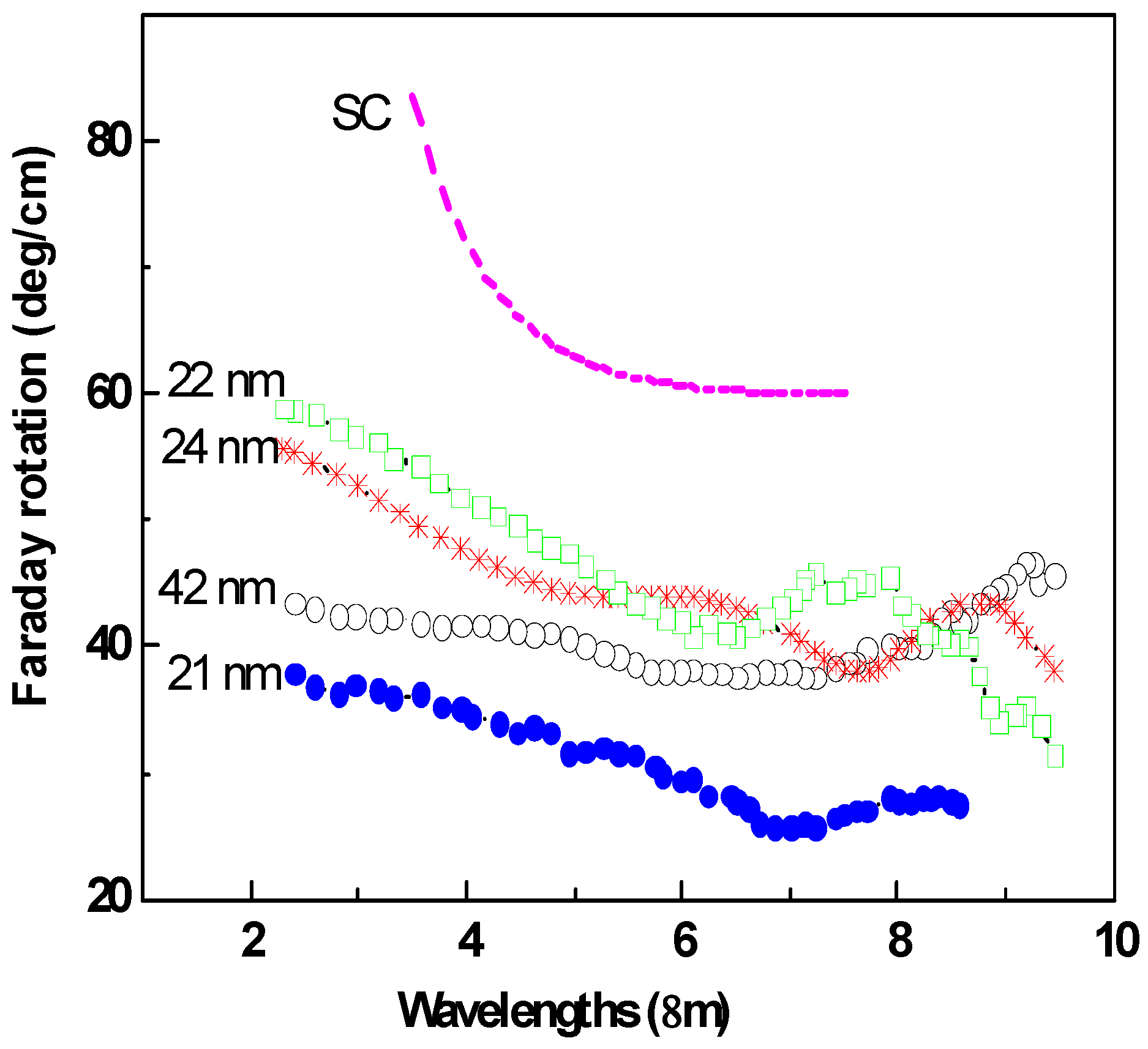
3.2. Nanocrystalline Y3Fe5O12 as a New Magneto-Optical Material
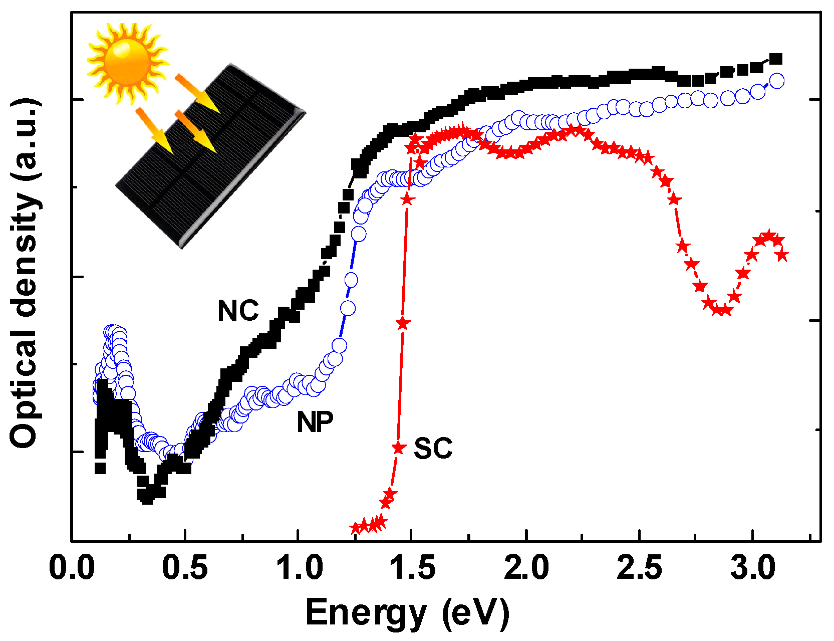
3.3. Nanocrystalline CuO as a Material for Selective Solar Energy Absorbers
4. THz Magnetooptics in Magnetic Semiconductors
5. Conclusions
Author Contributions
Funding
Institutional Review Board Statement
Informed Consent Statement
Data Availability Statement
Acknowledgments
Conflicts of Interest
References
- Methfessel, S.; Mattis, D.C. Magnetic Semiconductors; Wijn, H.P.J., Ed.; Springer: Berlin/Heidelberg, Germany; New York, NY, USA, 1968; pp. 389–562. [Google Scholar] [CrossRef]
- Seeger, K. Semiconductor Physics; Springer Science & Business Media: Berlin/Heidelberg, Germany, 2013. [Google Scholar]
- Nagaev, E.L. Physics of Magnetic Semiconductor; Mir Publishers: Moscow, Russia, 1983; p. 388. [Google Scholar]
- Grundmann, M. Physics of Semiconductors; Springer: Berlin/Heidelberg, Germany, 2010; pp. 401–472. [Google Scholar]
- Belov, K.P.; Tretyakov, Y.D.; Gordeev, I.V.; Koroleva, L.I.; Kesler, Y.A. Magnetic Semiconductors—Chalcogenide Spinels; Moscow State University: Moscow, Russia, 1981. [Google Scholar]
- Nagaev, E.L. Colossal Magnetoresistance and Phase Separation in Magnetic Semiconductors; Imperial College Press: London, UK, 2002; p. 1. [Google Scholar]
- Koroleva, L.I. Magnetic Semiconductors; Moscow State University: Moscow, Russia, 2003. [Google Scholar]
- Barner, K. New Trends in the Characterization of CMR-Manganites and Related Materials; Research Signpost: Gottingen, Germany, 2005; p. 1. [Google Scholar]
- Dionne, G.F. Magnetic Oxides; Springer: New York, NY, USA, 2009; p. 15. [Google Scholar]
- Zvezdin, A.K.; Kotov, V.A. Modern Magnetooptics and Magnetooptical Materials; CRC Press: Boca Raton, FL, USA, 1997. [Google Scholar]
- Telegin, A.V.; Sukhorukov, Y.P.; Bessonov, V.D.; Naumov, S.V. The Faraday effect in CoFe2O4 spinel ferrite in the IR range. Tech. Phys. Lett. 2019, 45, 601–604. [Google Scholar] [CrossRef]
- Kimel, A.; Zvezdin, A.; Sharma, S.; Shallcross, S.; De Sousa, N.; Garcia-Martin, A.; Vavassori, P. The 2022 magneto-optics roadmap. J. Phys. D Appl. Phys. 2022, 55, 463003. [Google Scholar] [CrossRef]
- Fumagalli, P.; Schoenes, J. Magneto-Optics; De Gruyter: Berlin, Germany, 2021. [Google Scholar] [CrossRef]
- Telegin, A.V.; Sukhorukov, Y.P.; Loshkareva, N.N.; Mostovshchikova, E.V.; Bebenin, N.G.; Gan’shina, E.A.; Granovsky, A.B. Giant magnetotransmission and magnetoreflection in ferromagnetic materials. JMMM 2015, 383, 104–109. [Google Scholar] [CrossRef]
- Morgunov, R.B.; Dmitriev, A.I. Spin dynamics in magnetic semiconductor nanostructures. Phys. Solid State 2009, 51, 1985. [Google Scholar] [CrossRef]
- Fetisov, Y.K.; Sigov, A.S. Spintronics: Physical foundations and devices. Radioelektron. Nanosistemy Inf. Tehnol. RENSIT 2018, 10, 343–356. [Google Scholar] [CrossRef]
- Sato, K.; Katayama-Yoshida, H. Design of colossal solubility of magnetic impurities for semiconductor spintronics by the Co-doping method. Jpn. J. Appl. Phys. 2007, 46, L1120. [Google Scholar] [CrossRef]
- Volkov, N.V. Spintronics: Manganite-based magnetic tunnel structures. Phys. Uspekhi 2012, 55, 250. [Google Scholar] [CrossRef]
- Ivanov, V.A. Diluted magnetic semiconductors and spintronics. Bull. Russ. Acad. Sci. Phys. 2007, 71, 1610–1612. [Google Scholar] [CrossRef]
- Yamada, Y.; Ueno, K.; Fukumura, T.; Yuan, H.T.; Shimotani, H.; Iwasa, Y.; Kawasaki, M. Electrically induced ferromagnetism at room temperature in cobalt-doped titanium dioxide. Science 2011, 332, 1065–1067. [Google Scholar] [CrossRef]
- Rizal, C.; Shimizu, H.; Mejía-Salazar, J.R. Magneto-Optics effects: New trends and future prospects for technological developments. Magnetochemistry 2022, 8, 94. [Google Scholar] [CrossRef]
- Awschalom, D.D.; Flatté, M.E. Challenges for semiconductor spintronics. Nat. Phys. 2007, 3, 153–159. [Google Scholar] [CrossRef]
- Akinaga, H.; Ohno, H. Semiconductor spintronics. IEEE Trans. Nanotechnol. 2002, 1, 19–31. [Google Scholar] [CrossRef]
- Hirohata, A.; Sukegawa, H.; Yanagihara, H.; Žutić, I.; Seki, T.; Mizukami, S.; Swaminathan, R. Roadmap for emerging materials for spintronic device applications. IEEE Trans. Magn. 2015, 51, 1–11. [Google Scholar] [CrossRef]
- Bibes, M.; Barthelemy, A. Oxide spintronics. IEEE Trans. Electron Devices 2007, 54, 1003–1023. [Google Scholar] [CrossRef] [Green Version]
- Gschneidner, K.A.; Pecharsky, V.K.; Pecharsky, A.O. Recent developments in magnetocaloric materials. Rep. Prog. Phys. 2005, 68, 1479. [Google Scholar] [CrossRef]
- Loshkareva, N.N.; Sukhorukov, Y.P.; Gizhevskii, B.A.; Samokhvalov, A.A. Modulator of IR emission on magnetic semiconductors. Pisma V Zhurnal Tekhnicheskoi Fiz. 1989, 15, 83–86. (In Russian) [Google Scholar]
- Loshkareva, N.N.; Sukhorukov, Y.P.; Samokhvalov, A.A.; Shuvalov, V.A.; Kartashev, E.V.; Chebotaev, N.M.; Naumov, S.V.; Aminov, T.G. Magnet-controlled band IR filter. Pisma V Zhurnal Tekhnicheskoi Fiz. 1992, 18, 10–13. (In Russian) [Google Scholar]
- Sukhorukov, Y.P.; Loshkareva, N.N.; Samokhvalov, A.A.; Tugushev, S.N. Magnetooptic infrared modulator in the Voigt geometry. Tech. Phys. Lett. 1996, 22, 43–45. [Google Scholar]
- Sukhorukov, Y.P.; Loshkareva, N.N.; Gan’shina, E.A.; Kaul, A.R.; Gorbenko, O.Y.; Fatieva, K.A. Giant change in the optical absorption of an La0.35Pr0.35Ca0.3MnO3 film near a metal-insulator transition and its possible application. Tech. Phys. Lett. 1999, 25, 551–554. [Google Scholar] [CrossRef]
- Sukhorukov, Y.P.; Loshkareva, N.N.; Telegin, A.V.; Mostovshchikova, E.V.; Kuznetsov, V.L.; Kaul, A.R.; Vinogradov, A.N. IR radiation modulator based on the effect of magnetotransmission in lanthanum manganite operating near room temperature. Tech. Phys. Lett. 2003, 29, 904–906. [Google Scholar] [CrossRef]
- Goyal, A.; Rajeswari, M.; Shreekala, R.; Lofland, S.E.; Bhagat, S.M.; Boettcher, T.; Kwon, C.; Ramesh, R.; Venkatesan, T. Material characteristics of perovskite manganese oxide thin films for bolometric applications. Appl. Phys. Lett. 1997, 71, 2535–2537. [Google Scholar] [CrossRef]
- Heiras, J.; Pichardo, E.; Mahmood, A.; López, T.; Pérez-Salas, R.; Siqueiros, J.M.; Blanco, O.; Castellanos, M. Thermochromism in (Ba,Sr)-Mn oxides. J. Phys. Chem. Solids 2002, 63, 591–595. [Google Scholar] [CrossRef]
- Sinitsyn, V.V.; Burmistrov, I.N.; Abrosimova, G.E.; Klinkova, L.A.; Bredikhin, S.I. Phase transitions and ionic conductivity of BaBixO1.5x+1 (x ≥ 5) oxides. Ionics 2006, 12, 69–71. [Google Scholar] [CrossRef]
- Burmistrov, I.N.; Droshshin, O.A.; Istomin, S.Y.; Sinitsyn, V.V.; Antipov, E.V.; Bredikhin, S.I. Sr0.75Y0.25Co0.5Mn0.5O3 − y perovskite cathode for solid oxide fuel cells. J. Electrochem. Soc. 2009, 156, 1212. [Google Scholar] [CrossRef]
- Martinez-Boubeta, C.; Simeonidis, K.; Oró, J.; Makridis, A.; Serantes, D.; Balcells, L. Finding the limits of magnetic hyperthermia on core-shell nanoparticles fabricated by physical vapor methods. Magnetochemistry 2021, 7, 49. [Google Scholar] [CrossRef]
- Moroz, P.; Jones, S.K.; Gray, B.N. Magnetically mediated hyperthermia: Current status and future directions. Int. J. Hyperth. 2002, 18, 267. [Google Scholar] [CrossRef]
- Kuznetsov, A.A.; Shlyakhtin, O.A.; Brusentsov, N.A.; Kuznetsov, O.A. Smart mediators for self-controlled inductive heating. Eur. Cells Mater. 2002, 3, 75–77. [Google Scholar]
- Pollert, E.; Knižek, K.; Maryško, M.; Kašpar, P.; Vasseur, S.; Duguet, E. New Tc-tuned magnetic nanoparticles for self-controlled hyperthermia. JMMM 2007, 316, 122–125. [Google Scholar] [CrossRef]
- Melnikov, O.V.; Gorbenko, O.Y.; Markelova, M.N.; Kaul, A.R.; Atsarkin, V.A.; Demidov, V.V.; Soto, C.; Roy, E.J.; Odintsov, B.M. Ag-doped manganite nanoparticles: New materials for temperature-controlled medical hyperthermia. J. Biomed. Mater. Res. 2009, 91A, 1048–1055. [Google Scholar] [CrossRef]
- Kessler, J. Polarized Electrons; Springer Science & Business Media: Berlin/Heidelberg, Germany, 2013; p. 299. [Google Scholar]
- Gregg, J.F.; Petej, I.; Jouguelet, E.; Dennis, C. Spin electronics—A review. J. Phys. D Appl. Phys. 2002, 35, R121. [Google Scholar] [CrossRef]
- Parkin, S.; Jiang, X.; Kaiser, C.; Panchula, A.; Roche, K.; Samant, M. Magnetically engineered spintronic sensors and memory. Proc. IEEE 2003, 91, 661–680. [Google Scholar] [CrossRef]
- Borukhovich, A.S. Quantum tunneling in multilayers and heterostructures with ferromagnetic semiconductors. Phys. Uspekhi 1999, 42, 653. [Google Scholar] [CrossRef]
- Zutic, I.; Fabian, J.; Das Sarma, S. Spintronics: Fundamentals and applications. Rev. Mod. Phys. 2004, 76, 323. [Google Scholar] [CrossRef] [Green Version]
- Ziese, M. Extrinsic magnetotransport phenomena in ferromagnetic oxides. Rep. Prog. Phys. 2002, 65, 143. [Google Scholar] [CrossRef]
- Dorr, K. Ferromagnetic manganites: Spin-polarized conduction versus competing interactions. J. Appl. Phys. 2006, 39, R125. [Google Scholar] [CrossRef]
- Haghiri-Gosnet, A.-M.; Renard, J.-P. CMR manganites: Physics, thin films and devices. J. Appl. Phys. 2003, 36, R127. [Google Scholar] [CrossRef]
- Ohring, M. Materials Science of Thin Films: Depositon & Structure; Elsevier: Amsterdam, The Netherlands, 2001. [Google Scholar]
- Kodama, R.H. Magnetic nanoparticles. JMMM 1999, 200, 359–372. [Google Scholar] [CrossRef]
- Arbuzova, T.I.; Gizhevskii, B.A.; Naumov, S.V.; Korolev, A.V.; Arbuzov, V.L.; Shal’nov, K.V.; Druzhkov, A.P. Temporal changes in magnetic properties of high-density CuO nanoceramics. JMMM 2003, 258, 342–344. [Google Scholar] [CrossRef]
- Osipov, V.V.; Viglin, N.A.; Kochev, V.; Samokhvalov, A.A. Microwave absorption at a junction between the ferromagnetic semiconductor HgCr,Se. JETP Lett. 1990, 52, 386–389. [Google Scholar]
- Borukhovich, A.S.; Viglin, N.A.; Osipov, V.V. Spin-polarized transport and submillimetric microwave spectroscopy of solids. Phys. Solid State 2002, 44, 938–945. [Google Scholar] [CrossRef]
- Watts, S.M.; van Wee, B.J. A solid state paramagnetic maser device driven by electron spin injection. Phys. Rev. Lett. 2006, 97, 116601. [Google Scholar] [CrossRef] [PubMed] [Green Version]
- Viglin, N.A.; Ustinov, V.V.; Osipov, V.V. Spin injection maser. JETP Lett. 2007, 86, 193–196. [Google Scholar] [CrossRef]
- Viglin, N.A.; Ustinov, V.V. Solid-State Conduction-Electron Maser. Russian Federation patent No 2007126305, 10 July 2007. (In Russian). Available online: https://rusneb.ru/catalog/000224_000128_0002351045_20090327_C1_RU/ (accessed on 10 September 2022).
- Osipov, V.V.; Viglin, N.A. Spin injection and spin transport in a ferromagnet-semiconductor junction: Microwave emission and absorption. J. Commun. Technol. Electron. 2003, 48, 548–558. [Google Scholar]
- Viglin, N.A.; Osipov, V.V.; Samokhvalov, A.A.; Naumov, S.V.; Borukhovich, A.S.; Denisov, O.F. Heterostructure Heusler alloy Co2MnSn-nSnSb: Emission in the millimeter and submillimeter microwave range. Phys. Low-Dimens. Semicond. Struct. 2000, 1–2, 29–36. [Google Scholar]
- Osipov, V.V.; Viglin, N.A.; Samokhvalov, A.A. Investigation of heterostructure “ferromagnetic semiconductor-semiconductor” in the millimeter and submillimeter microwave range. Phys. Lett. A 1998, 247, 353–359. [Google Scholar] [CrossRef]
- Papaconstatopoulos, D.A.; Pikett, W.E. Tight-binding coherent potential approximation study of ferromagnetic La2/3Ba1/3MnO3. Phys. Rev. B 1998, 57, 12751. [Google Scholar] [CrossRef] [Green Version]
- Irkhin, V.Y.; Katsnel’son, M.I. Half-metallic ferromagnets. Physics-Uspekhi 1994, 37, 659–676. [Google Scholar] [CrossRef]
- Fiederling, R.; Keim, M.; Reuscher, G.A.; Ossau, W.; Schmidt, G.; Waag, A.; Molenkamp, L.W. Injection and detection of a spin-polarized current in a light-emitting diode. Nature 1999, 402, 787–790. [Google Scholar] [CrossRef]
- Ohno, H.; Chiba, A.D.; Matsukura, A.F.; Omiya, T.; Abe, E.; Dietl, T.; Ohtani, K. Electric-field control of ferromagnetism. Nature 2000, 408, 944–946. [Google Scholar] [CrossRef]
- Bebenin, N.G.; Ustinov, V.V. Inverse spin population near ferromagnet/nonmagnetic semiconductor contact. JMMM 2004, 272, 1917–1918. [Google Scholar] [CrossRef]
- Samokhvalov, A.A.; Osipov, V.V.; Solin, N.I.; Gunichev, A.F.; Korenblit, I.A.; Galdikas, A.P. Electron-magnon interaction in magnetic semiconductors. JMMM 1984, 46, 191–198. [Google Scholar] [CrossRef]
- Solin, N.I.; Samokhvalov, A.A. Influence of a strong electric field on microwave absorption in a ferromagnetic semiconductor Cd1−xAgxCr2Se4. Sov. Phys. Solid State 1976, 18, 1226–1227. [Google Scholar]
- Samokhvalov, A.A.; Sukhorukov, Y.P. Effect of hot carriers on the Raman spectra of the magnetic semiconductors CdCr2Se4 and HgCr2Se4. JETP Lett. 1982, 35, 212. [Google Scholar]
- Akhiezer, A.I.; Bar’Yakhtar, V.G.; Peletminskii, S.V. Coherent amplification of spin waves. Phys. Lett. 1963, 4, 129–130. [Google Scholar] [CrossRef]
- Auslender, M.I.; Samokhvalov, A.A.; Solin, N.I.; Shumilov, I.Y. Cherenkov interaction of spin waves with charge carriers in the ferromagnetic semiconductor HgCr2Se4. Sov. Phys. JETP 1988, 67, 2516–2521. [Google Scholar]
- Solin, N.I.; Samokhvalov, A.A.; Shumilov, I.Y. Intensification of magnetostatic and spin waves by the drifting charge carriers in a magnetic semiconductor HgCr2Se4. JETP Lett. 1987, 44, 597–600. [Google Scholar]
- Samokhvalov, A.A.; Solin, N.I.; Viglin, N.A.; Kostylev, V.A.; Osipov, V.V.; Babushkin, V.S. Electron-magnon interaction in magnetic semiconductors. Phys. Status Solidi B 1992, 169, k93–k98. [Google Scholar] [CrossRef]
- Nagaev, E.L. Magnetoelectric waves. Sov. JETP Lett. 1987, 45, 156. [Google Scholar]
- Khitun, A.; Nikonov, D.E.; Kang, L.W. Magnetoelectric spin wave amplifier for spin wave logic circuits. J. Appl. Phys. 2009, 106, 123909. [Google Scholar] [CrossRef] [Green Version]
- Solin, N.I.; Naumov, S.V.; Samokhvalov, A.A. Interface phenomena and microwave magnetoresistance in polycrystalline La1−xCaxMnO3 lanthanum manganites. Phys. Solid State 2000, 42, 925–930. [Google Scholar] [CrossRef]
- Solin, N.I.; Ustinov, V.V.; Naumov, S.V. Colossal magnetoresistance of the inhomogeneous ferromagnetic semiconductor HgCr2Se4. Phys. Solid State 2008, 50, 901–908. [Google Scholar] [CrossRef]
- Mitra, C.; Raychaudhuri, P.; Köbernik, G.; Dörr, K.; Müller, K.H.; Schultz, L.; Pinto, R. P–n diode with hole-and electron-doped lanthanum manganites. Appl. Phys. Lett. 2001, 79, 2408–2410. [Google Scholar] [CrossRef] [Green Version]
- Kaul, A.R.; Gorbenko, O.Y.; Kamenev, A.A. The role of heteroepitaxy in the development of new thin-film oxide-based functional materials. Russ. Chem. Rev. 2004, 73, 861–880. [Google Scholar] [CrossRef]
- Sukhorukov, Y.P.; Telegin, A.V.; Gan’shina, E.A.; Loshkareva, N.N.; Kaul, A.R.; Gorbenko, O.Y.; Mel’nikov, O.V.; Vinogradov, A.N. Tunneling of spin-polarized charge carriers in La0.8Ag0.1MnO3+δ film with variant structure: Magnetotransport and magnetooptical data. Tech. Phys. Lett. 2005, 31, 484–487. [Google Scholar] [CrossRef]
- Gan’shina, E.; Loshkareva, N.; Sukhorukov, Y.; Mostovshchikova, E.; Vinogradov, A.; Nomerovannaya, L. Optical and magneto-optical spectroscopy of manganites. JMMM 2006, 300, 62–66. [Google Scholar] [CrossRef]
- Sukhorukov, Y.P.; Gan’Shina, E.A.; Belevtsev, B.I.; Loshkareva, N.N.; Vinogradov, A.N.; Rathnayaka, K.D.D.; Naugle, D.G. Giant change in infrared light transmission in La0.67Ca0.33MnO3 film near the Curie temperature. J. Appl. Phys. 2002, 91, 4403–4408. [Google Scholar] [CrossRef] [Green Version]
- Granovsky, A.; Sukhorukov, Y.; Gan’shina, E.; Telegin, A. Magnetorefractive effect in magnetoresistive materials. In Magnetophotonics; Springer: Berlin/Heidelberg, Germany, 2013; pp. 107–133. [Google Scholar]
- Loshkareva, N.N.; Solin, N.I.; Sukhorukov, Y.P.; Lobachevskaya, N.I.; Panfilova, E.V. Optical spectroscopy of phase separation in LaxMnO3. Phys. B Condens. Matter 2001, 293, 390–393. [Google Scholar] [CrossRef]
- Sarychev, A.K.; Boyarintsev, S.O.; Rakhmanov, A.L.; Kugel, K.I.; Sukhorukov, Y.P. Collective volume plasmons in manganites with nanoscale phase separation: Simulation of the measured infrared spectra of La0.7Ca0.3MnO3. Phys. Rev. Lett. 2011, 107, 267401. [Google Scholar] [CrossRef]
- Melnikov, O.V.; Sukhorukov, Y.P.; Telegin, A.V.; Gan’shina, E.A.; Loshkareva, N.N.; Kaul, A.R.; Smoljak, I.B. The evolution of magneto-transport and magneto-optical properties of thin La0.8Ag0.1MnO3+δ films possessing the in-plane variant structure as a function of the film thickness. J. Phys. Condens. Matter 2006, 18, 3753. [Google Scholar] [CrossRef]
- Sukhorukov, Y.P.; Gan’shina, E.A.; Kaul, A.R.; Gorbenko, O.Y.; Loshkareva, N.N.; Telegin, A.V.; Kartavtseva, M.S.; Vinogradov, A.N. Sm0.55Sr0.45MnO3/Nd0.55Sr0.45MnO3 heteroepitaxial structure: Optical and magnetotransport properties. Tech. Phys. 2008, 53, 716–721. [Google Scholar] [CrossRef]
- Sukhorukov, Y.P.; Telegin, A.V.; Nosov, A.P.; Gan’shina, E.A.; Stepantsov, E.A.; Lombardi, F.; Winkler, D. Magnetorefractive and Kerr effects in the [La0.67Ca0.33MnO3/La0.67Sr0.33MnO3]n superlattices. Superlattices Microstruct. 2014, 75, 680–691. [Google Scholar] [CrossRef]
- Sukhorukov, Y.P.; Loshkareva, N.N.; Gan’shina, E.A.; Kaul, A.R.; Kamenev, A.A.; Gorbenko, O.Y.; Telegin, A.V. Magnetotransmission and magnetoresistance in film manganite/ferrite heterostructures. Phys. Met. Metallogr. 2009, 107, 579–587. [Google Scholar] [CrossRef]
- Kaul, A.R.; Gorbenko, O.Y.; Loshkareva, N.N.; Sukhorukov, Y.P.; Mostovshchikova, E.V. Magnetic lens based on the ferromagnetic manganites with high TC-superconductor heterostructure. Phys. Low Dimens. Semicond. Struct. 2003, 7, 124–129. [Google Scholar]
- Gorbenko, O.Y.; Kaul, A.R.; Mel’nikov, O.V.; Gan’shina, E.A.; Ganin, A.Y.; Sukhorukov, Y.P.; Mostovshchikova, E.V. Synthetic routes to colossal magnetoresistance manganites thin films containing unstable or highly volatile metal oxides. Thin Solid Film. 2007, 515, 6395–6401. [Google Scholar] [CrossRef]
- Zhao, T.; Scholl, A.; Zavaliche, F.; Lee, K.; Barry, M.; Doran, A.; Ramesh, R. Electrical control of antiferromagnetic domains in multiferroic BiFeO3 films at room temperature. Nat. Mater. 2006, 5, 823–829. [Google Scholar] [CrossRef] [PubMed]
- Wang, K.F.; Liu, J.M.; Ren, Z.F. Multiferroicity: The coupling between magnetic and polarization orders. Adv. Phys. 2009, 58, 321–448. [Google Scholar] [CrossRef]
- Inoue, M.; Fujikawa, R.; Baryshev, A.; Khanikaev, A.; Lim, P.B.; Uchida, H.; Aktsipetrov, O.; Fedyanin, A.; Murzina, T.; Granovsky, A. Magnetophotonic crystals. J. Phys. D Appl. Phys. 2006, 39, R151. [Google Scholar] [CrossRef]
- Sukhorukov, Y.P.; Gizhevskii, B.A.; Loshkareva, N.N.; Gorbenko, O.Y.; Kaul, A.R.; Telegin, A.V. Infrared modulator. Russian Federation Patent No 2346315, Bull. No 4, 10 February 2009. (In Russian). Available online: https://rusneb.ru/catalog/000224_000128_0002346315_20090210_C1_RU/ (accessed on 2 September 2022).
- Bessonova, V.A.; Telegin, A.V.; Nosov, A.P.; Patrakov, E.I.; Makarova, M.V.; Sukhorukov, Y.P. Mid-infrared optical response to magnetic field in the La0.65Ba0.35MnO3 film grown by PLD. JMMM 2022, 564, 170030. [Google Scholar] [CrossRef]
- Granovskii, A.B.; Gan’shina, E.A.; Yurasov, A.N.; Boriskina, Y.V.; Yerokhin, S.G.; Khanikaev, A.B.; Inoue, M.; Vinogradov, A.P.; Sukhorukov, Y.P. Magnetorefractive effect in nanostructures, manganites, and magnetophotonic crystals based on these materials. J. Commun. Technol. Electron. 2007, 52, 1065–1071. [Google Scholar] [CrossRef]
- Sukhorukov, Y.P.; Telegin, A.V.; Loshkareva, N.N.; Kaul, A.R.; Gan’shina, E.A. Infrared Modulator. Russian Federation Patent No 88165, Bull. No 30, 27 October 2009. (In Russian). Available online: https://rusneb.ru/catalog/000224_000128_0000088165_20091027_U1_RU/ (accessed on 9 September 2022).
- Yurasov, A.N.; Boriskina, Y.V.; Gan’shina, E.A.; Granovsky, A.B.; Sukhorukov, Y.P. Magnetorefractive effect in manganites. Phys. Solid State 2007, 49, 1121–1124. [Google Scholar] [CrossRef]
- Sukhorukov, Y.P.; Telegin, A.V.; Gan’shina, E.A. Simultaneous controlling the intensity of reflected and transmitted light in thin films of manganites. Tech. Phys. 2021, 66, 942–946. [Google Scholar] [CrossRef]
- Sukhorukov, Y.P.; Telegin, A.V.; Granovsky, A.B.; Gan’shina, E.A.; Zhukov, A.; Gonzalez, J.; Herranze, G.; Caicedo, J.M.; Yurasov, A.N.; Bessonov, V.D.; et al. Magnetorefractive effect in manganites with a colossal magnetoresistance in the visible spectral region. JETP 2012, 114, 141–149. [Google Scholar] [CrossRef]
- Formisano, F.; Medapalli, R.; Xiao, Y.; Ren, H.; Fullerton, E.E.; Kimel, A.V. Femtosecond magneto-optics of EuO. JMMM 2020, 502, 166479. [Google Scholar] [CrossRef]
- van Kooten, S.C.P.; Springholz, G.; Henriques, A.B. Direct optical probing of ultrafast spin dynamics in a magnetic semiconductor. Phys. Rev. B 2022, 105, 224427. [Google Scholar] [CrossRef]
- Ishihara, S. Photoinduced ultrafast phenomena in correlated electron magnets. J. Phys. Soc. Jpn. 2019, 88, 072001. [Google Scholar] [CrossRef]
- Sukhorukov, Y.P.; Moskvin, A.M.; Loshkareva, N.N.; Smolyak, I.B.; Arkhipov, V.E.; Mukovskii, Y.M.; Shmatok, A.V. Magnetooptical Faraday effect in La0.7Sr0. 3MnO3−δ films. Tech. Phys. 2001, 46, 778–781. [Google Scholar] [CrossRef]
- Park, J.H.; Takagi, H.; Nishimura, K.; Uchida, H.; Inoue, M.; Park, J.H.; Cho, J.K. Magneto-optic spatial light modulators driven by an electric field. J. Appl. Phys. 2003, 93, 8525–8527. [Google Scholar] [CrossRef]
- Park, J.H.; Sung, I.K.; Cho, J.K.; Nishimura, K.; Uchida, H.; Inoue, M. Flat-surface pixel for magneto-optic spatial light modulator. IEEE Trans. Magn. 2003, 39, 3169–3171. [Google Scholar] [CrossRef]
- Park, J.H.; Kim, J.H.; Cho, J.K.; Nishimura, K.; Uchida, H.; Inoue, M. An optical micro-magnetic display. JMMM 2004, 272, 2260–2262. [Google Scholar] [CrossRef]
- Bukharaev, A.A.; Zvezdin, A.K.; Pyatakov, A.P.; Fetisov, Y.K. Straintronics: A new trend in micro- and nanoelectronics and materials science. Physics-Uspekhi 2018, 61, 1175. [Google Scholar] [CrossRef]
- Sukhorukov, Y.P.; Telegin, A.V.; Bebenin, N.G.; Nosov, A.P.; Bessonov, V.D.; Buchkevich, A.A. Strain-magneto-optics of a magnetostrictive ferrimagnetic CoFe2O4. Solid State Commun. 2017, 263, 27–30. [Google Scholar] [CrossRef]
- Sukhorukov, Y.; Telegin, A.; Bebenin, N.; Bessonov, V.; Naumov, S.; Shishkin, D.; Nosov, A. Strain-magnetooptics in single crystals of CoFe2O4. Magnetochemistry 2022, 8, 135. [Google Scholar] [CrossRef]
- Telegin, A.V.; Sukhorukov, Y.P.; Bebenin, N.G. Anisotropic magnetoabsorption of light in cobalt ferrite and its correlation with magnetostriction. JETP 2020, 131, 970–975. [Google Scholar] [CrossRef]
- Sukhorukov, Y.P.; Telegin, A.V.; Bebenin, N.G.; Nosov, A.P.; Bessonov, V.D.; Buchkevich, A.A.; Patrakov, E.I. Magnetoreflection and magnetostriction in ferrimagnetic spinels CoFe2O4. J. Exp. Theor. Phys. 2018, 126, 106–114. [Google Scholar] [CrossRef]
- Nasirpouri, F.; Nogaret, A. (Eds.) Nanomagnetism and Spintronics: Fabrication, Materials, Characterization and Applications; World Scientific: Singapore, 2010; 400p. [Google Scholar]
- Zimnyakova, P.E.; Ignatyeva, D.O.; Karki, D.; Voronov, A.A.; Shaposhnikov, A.N.; Berzhansky, V.N.; Belotelov, V.I. Two-dimensional array of iron-garnet nanocylinders supporting localized and lattice modes for the broadband boosted magneto-optics. Nanophotonics 2022, 11, 119–127. [Google Scholar] [CrossRef]
- Omelyanchik, A.; Villa, S.; Singh, G.; Rodionova, V.; Laureti, S.; Canepa, F.; Peddis, D. Magnetic properties of Bi-magnetic core/shell nanoparticles: The case of thin shells. Magnetochemistry 2021, 7, 146. [Google Scholar] [CrossRef]
- Gupta, A.; Zhang, R.; Kumar, P.; Kumar, V.; Kumar, A. Nano-structured dilute magnetic semiconductors for efficient spintronics at room temperature. Magnetochemistry 2020, 6, 15. [Google Scholar] [CrossRef] [Green Version]
- Dmitriev, A.I.; Talantsev, A.D.; Zaitsev, S.V.; Koplak, O.V.; Morgunov, R.B. Nano-and heterostructures of magnetic semiconductors for spintronics. Russ. Chem. Bull. 2011, 60, 1051–1057. [Google Scholar] [CrossRef]
- Silva, A.S.; Guimarães, É.V.; Sales, T.O.; Silva, W.S.; Batista, E.A.; Jacinto, C.; Silva, R.S. Nanostructured magnetic semiconductors. In Fundamentals of Low Dimensional Magnets; CRC Press: Boca Raton, FL, USA, 2022; pp. 23–39. [Google Scholar]
- Kotnala, R.K.; Shah, J. Ferrite materials: Nano to spintronics regime. In Handbook of Magnetic Materials; Elsevier: Amsterdam, The Netherlands, 2015; Volume 23, pp. 291–379. [Google Scholar] [CrossRef]
- Loshkareva, N.N.; Sukhorukov, Y.P.; Gizhevskii, B.A.; Naumov, S.V.; Samokhvalov, A.A.; Moskvin, A.S.; Belykh, T.A. Polar-center phase nuclei in He+-irradiated CuO single crystals. Phys. Solid State 1998, 40, 383–388. [Google Scholar] [CrossRef]
- Lin, H.H.; Wang, C.Y.; Shih, H.C.; Chen, J.M.; Hsieh, C.T. Characterizing well-ordered CuO nanofibrils synthesized through gas-solid reactions. J. Appl. Phys. 2004, 95, 5889–5895. [Google Scholar] [CrossRef]
- Baru, V.G.; Volkenshtein, F.F. Influence of Irradiation on the Surface Properties of Semiconductors; Nauka: Moscow, Russia, 1978. [Google Scholar]
- Yermakov, A.Y.; Feduschak, T.A.; Sedoi, V.S.; Uimin, M.A.; Mysik, A.A. Magneto-modified catalyst on the base of nanocrystalline CuO. JMMM 2004, 272, 2445–2447. [Google Scholar] [CrossRef]
- Morales, J.; Sánchez, L.; Martín, F.; Ramos-Barrado, J.R.; Sánchez, M. Nanostructured CuO thin film electrodes prepared by spray pyrolysis: A simple method for enhancing the electrochemical performance of CuO in lithium cells. Electrochim. Acta 2004, 49, 4589–4597. [Google Scholar] [CrossRef]
- Wei, Q.; Luo, W.D.; Liao, B.; Liu, Y.; Wang, G. Giant capacitance effect and physical model of nano crystalline CuO–BaTiO3 semiconductor as a CO2 gas sensor. J. Appl. Phys. 2000, 88, 4818–4824. [Google Scholar] [CrossRef]
- Pilyugin, V.P.; Gizhevskii, B.A.; Patselov, A.M.; Chernyshev, E.G.; Lisin, V.L. Plastic deformation Chamber at Low Temperatures. Russian Federation patent No 61882, Bull. No 7, 10 March 2007. Available online: https://rusneb.ru/catalog/000224_000128_0000061882_20070310_U1_RU/ (accessed on 11 September 2022).
- Pilyugin, V.P.; Chernyshev, E.G.; Patselov, A.M.; Gizhevskii, B.A. High Pressure Chamber for Spectroscopic Analysis. Russian Federation Patent No 60727, Bull. No 3, 27 January 2007. (In Russian). Available online: https://rusneb.ru/catalog/000224_000128_0000060727_20070127_U1_RU/ (accessed on 11 September 2022).
- Arbuzova, T.I.; Voronin, V.I.; Gizhevskii, B.A.; Naumov, S.V.; Arbuzov, V.L. An inhomogeneous paramagnetic state of the LaMnO3+δ nanoceramics prepared by shock-wave loading. Phys. Solid State 2010, 52, 1217–1226. [Google Scholar] [CrossRef]
- Gizhevskii, B.A.; Galakhov, V.R.; Kozlov, E.A. Effects of shock-wave loading in oxides. Petrology 2012, 20, 317–330. [Google Scholar] [CrossRef]
- Gizhevskii, B.A.; Sukhorukov, Y.P.; Moskvin, A.S.; Loshkareva, N.N.; Mostovshchikova, E.V.; Ermakov, A.E.; Gaviko, V.S. Anomalies in the optical properties of nanocrystalline copper oxides CuO and Cu2O near the fundamental absorption edge. JETP 2006, 102, 297–302. [Google Scholar] [CrossRef]
- Krynetskii, I.B.; Gizhevskii, B.A.; Naumov, S.V.; Kozlov, E.A. Size effect of the thermal expansion of nanostructural copper oxide. Phys. Solid State 2008, 50, 756–758. [Google Scholar] [CrossRef]
- Vykhodets, V.B.; Vykhodets, E.V.; Gizhevskii, B.A.; Zakharov, R.G.; Kozlov, E.A.; Kurennykh, T.E.; Petrova, S.A.; Trakhtenberg, I.S.; Fishman, A.Y. Grain boundary self-diffusion of tracer 18O atoms in nanocrystalline oxide LaMnO3+δ. JETP Lett. 2008, 87, 115–119. [Google Scholar] [CrossRef]
- Arbuzova, T.I.; Naumov, S.V.; Kozlov, E.A.; Arbuzov, V.L.; Shal’nov, K.V.; Gizhevskii, B.A.; Voronin, V.I. Influence of structural defects on magnetic properties of the submicrometer ceramic Mn3O4. JETP 2006, 102, 931–937. [Google Scholar] [CrossRef]
- Gizhevsky, B.A.; Kozlov, E.A.; Ermakov, A.E.; Lukin, N.V.; Naumov, S.V.; Samokhvalov, A.A. Microstructure of CuO after shock-loading and milling. Phys. Met. Metallogr. 2001, 92, 153–157. [Google Scholar]
- Druzhkov, A.P.; Gizhevskii, B.A.; Arbuzov, V.L.; Kozlov, E.A.; Shalnov, K.V.; Naumov, S.V.; Perminov, D.A. Electronic and structural properties of micro-and nanometre-sized crystalline copper monoxide ceramics investigated by positron annihilation. J. Phys. Condens. Matter 2002, 14, 7981. [Google Scholar] [CrossRef]
- Gizhevskii, B.A.; Sukhorukov, Y.P.; Gan’shina, E.A.; Loshkareva, N.N.; Telegin, A.V.; Lobachevskaya, N.I.; Gaviko, V.S.; Pilyugin, V.P. Optical and magneto-optical properties of nanostructured yttrium iron garnet. Phys. Solid State 2009, 51, 1836–1842. [Google Scholar] [CrossRef]
- Makhnev, A.A.; Gizhevskii, B.A.; Nomerovannaya, L.V. Optical spectra of nanoceramics of yttrium-iron garnet Y3Fe5O12 obtained by the method of intense plastic deformation. JETP Lett. 2010, 91, 79–82. [Google Scholar] [CrossRef]
- Falkovskaya, L.D.; Fishman, A.Y.; Mitrofanov, V.Y.; Ivanov, M.A. Random fields in disordered magnetics with Jahn-Teller ions. In Proceedings of the Fifth International Conference on Mathematical Modeling and Computer Simulations of Materials Technologies, Ariel, Israel, 21–23 July 2015; pp. 1–202. [Google Scholar]
- Agnihotri, O.P.; Gupta, B.K. Solar Selective Surfaces; Wiley-Interscience: New York, NY, USA, 1981; 232p. [Google Scholar]
- Tesfamichael, T.; Hoel, A.; Wäckelgard, E.; Niklasson, G.A.; Gunde, M.K.; Orel, Z.C. Optical characterization and modeling of black pigments used in thickness-sensitive solar-selective absorbing paints. Sol. Energy 2001, 69, 35–43. [Google Scholar] [CrossRef]
- Van Buskirk, O.R. Solar Selective Surfaces. U.S. Patent No 4310596, 12 January 1982. Available online: https://www.freepatentsonline.com/4310596.html (accessed on 11 September 2022).
- Karlsson, B.; Ribbing, C.G.; Roos, A.; Valkonen, E.; Karlsson, T. Optical properties of some metal oxides in solar absorbers. Phys. Scr. 1982, 25, 826. [Google Scholar] [CrossRef]
- Sukhorukov, Y.P.; Gizhevskii, B.A.; Mostovshchikova, E.V.; Yermakov, A.Y.; Tugushev, S.N.; Kozlov, E.A. Nanocrystalline copper oxide for selective solar energy absorbers. Tech. Phys. Lett. 2006, 32, 132–135. [Google Scholar] [CrossRef]
- Ovchinnikov, S.G.; Gizhevskii, B.A.; Sukhorukov, Y.P.; Ermakov, A.E.; Uimin, M.A.; Kozlov, E.A.; Bagazeev, A.V. Specific features of the electronic structure and optical spectra of nanoparticles with strong electron correlations. Phys. Solid State 2007, 49, 1116–1120. [Google Scholar] [CrossRef]
- Shabatina, T.I.; Vernaya, O.I.; Shabatin, V.P.; Melnikov, M.Y. Magnetic nanoparticles for biomedical purposes: Modern trends and prospects. Magnetochemistry 2020, 6, 30. [Google Scholar] [CrossRef]
- Rempel, A.A. Nanotechnologies. Properties and applications of nanostructured materials. Russ. Chem. Rev. 2007, 76, 435. [Google Scholar] [CrossRef]
- Simovski, C.; Tretyakov, S. An Introduction to Metamaterials and Nanophotonics; Cambridge University Press: Cambridge, UK, 2020. [Google Scholar]
- Kumar, C.S. Magnetic Nanomaterials; John Wiley & Sons: Hoboken, NJ, USA, 2009. [Google Scholar]
- Kharat, P.B.; Somvanshi, S.B.; Jadhav, K.M. Multifunctional magnetic nano-platforms for advanced biomedical applications: A brief review. J. Phys. Conf. Ser. 2020, 1644, 012036. [Google Scholar] [CrossRef]
- Ishii, T.; Yamakawa, H.; Kanaki, T.; Miyamoto, T.; Kida, N.; Okamoto, H.; Ohya, S. Ultrafast magnetization modulation induced by the electric field component of a terahertz pulse in a ferromagnetic-semiconductor thin film. Sci. Rep. 2018, 8, 1–6. [Google Scholar] [CrossRef] [PubMed]
- Kimel, A.V.; Kalashnikova, A.M.; Pogrebna, A.; Zvezdin, A.K. Fundamentals and perspectives of ultrafast photoferroic recording. Phys. Rep. 2020, 852, 1–46. [Google Scholar] [CrossRef]
- Telegin, A.V.; Bebenin, N.G.; Zainullina, R.I.; Mostovshchikova, E.V.; Viglin, N.A.; Gan’shina, E.A.; Zykov, G.S.; Fedorov, V.A.; Menshchikova, T.K.; Buchkevich, A.A. Optical and magneto-optical effects in Hg1−xCdxCr2Se4 (0 ≤ x ≤ 1) single crystals. JETP 2015, 121, 437–445. [Google Scholar] [CrossRef]
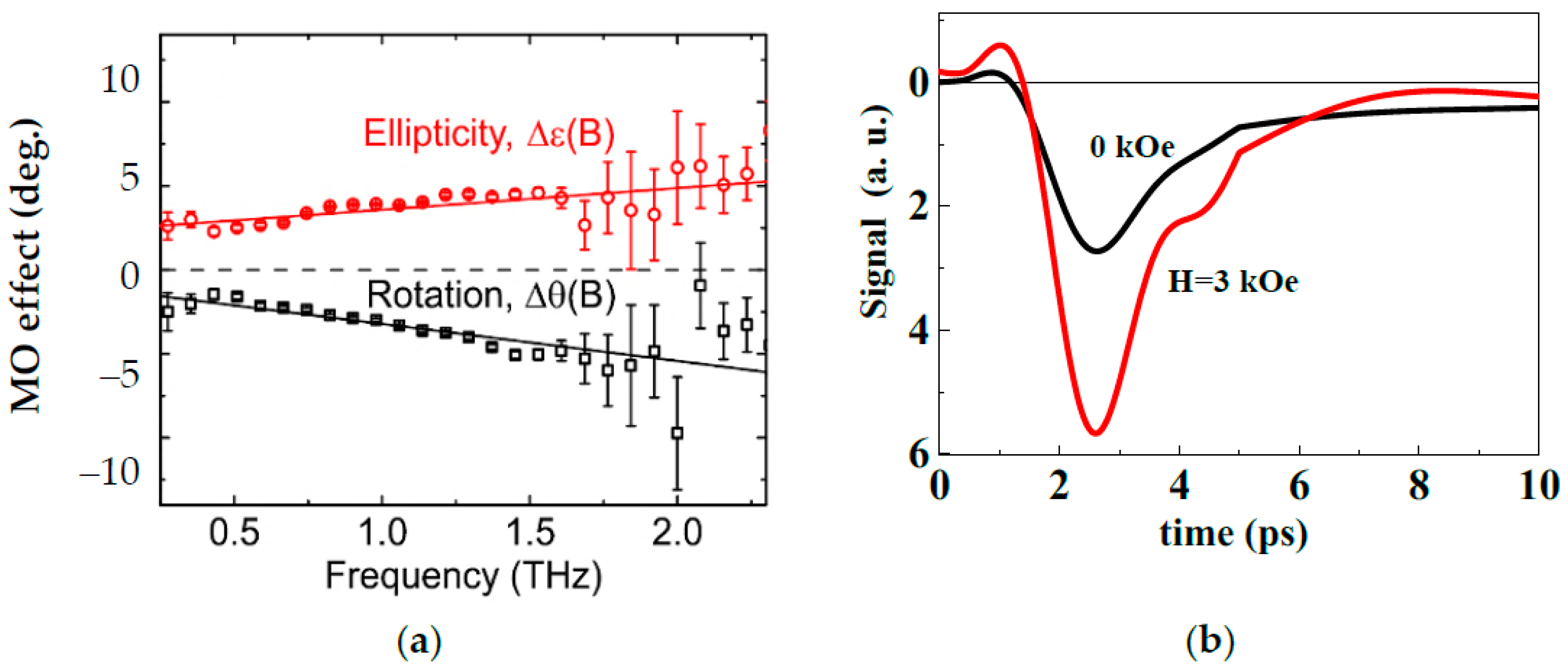
- Huisman, T.J.; Mikhaylovskiy, R.V.; Telegin, A.V.; Sukhorukov, Y.P.; Granovsky, A.B.; Naumov, S.V.; Rasing, T.; Kimel, A.V. Terahertz magneto-optics in the ferromagnetic semiconductor HgCdCr2Se4. Appl. Phys. Lett. 2015, 106, 132411. [Google Scholar] [CrossRef] [Green Version]
- Barsaume, S.; Telegin, A.V.; Sukhorukov, Y.P.; Stavrias, N.; Fedorov, V.A.; Menshchikova, T.K.; Rasing, T.; Kimel, A.V. Static and time-resolved mid-infrared spectroscopy of Hg0.95Cd0.05Cr2Se4 spinel. J. Phys. Condens. Matter 2017, 29, 325502–325508. [Google Scholar] [CrossRef] [PubMed] [Green Version]
- Pogrebna, A.; Barsaume, S.; Subkhangulov, R.R.; Telegin, A.V.; Sukhorukov, Y.P.; Chzhan, A.V.; Rasing, T.; Kimel, A.V. Spectral tunability of laser-induced spin dynamics in the ferromagnetic semiconductor CdCr2Se4. Phys. Rev. B 2018, 98, 214427–214433. [Google Scholar] [CrossRef]


| Film | MT, % | CMR, % | TC, K |
|---|---|---|---|
| La0.7Ca0.3MnO3 | 25 | 33 | 259 |
| (La0.75Pr0.25)0.7Ca0.3MnO3 | 25 | 45 | 214 |
| (La0.5Pr0.5)0.7Ca0.3MnO3 | 23 | 60 | 179 |
| (La0.25Pr0.75)0.7Ca0.3MnO3 | 4 | 21 | 79 |
| La0.67Sr0.33MnO3 | 6 | 8 | 356 |
| La0.67Ba0.33MnO3 | 10 | 25 | 306 |
| La0.8Ag0.1MnO3+δ | 11 | 8 | 301 |
| La0.85Ag0.15MnO3 | 9 | 17 | 316 |
| La0.82K0.18MnO3+δ | 6 | 19 | 280 |
Publisher’s Note: MDPI stays neutral with regard to jurisdictional claims in published maps and institutional affiliations. |
© 2022 by the authors. Licensee MDPI, Basel, Switzerland. This article is an open access article distributed under the terms and conditions of the Creative Commons Attribution (CC BY) license (https://creativecommons.org/licenses/by/4.0/).
Share and Cite
Telegin, A.; Sukhorukov, Y. Magnetic Semiconductors as Materials for Spintronics. Magnetochemistry 2022, 8, 173. https://doi.org/10.3390/magnetochemistry8120173
Telegin A, Sukhorukov Y. Magnetic Semiconductors as Materials for Spintronics. Magnetochemistry. 2022; 8(12):173. https://doi.org/10.3390/magnetochemistry8120173
Chicago/Turabian StyleTelegin, Andrei, and Yurii Sukhorukov. 2022. "Magnetic Semiconductors as Materials for Spintronics" Magnetochemistry 8, no. 12: 173. https://doi.org/10.3390/magnetochemistry8120173