Article

Estimation of the Electricity Storage Volume Density of Compact SMESs of a New Concept Based on Si Microfabrication Technologies

1
Institutes of Innovation for Future Society, Nagoya University, Furo-cho, Chikusa-ku, Nagoya 464-8603, Japan
2
Toyota Technological Institute, Graduate School of Engineering, Hisakata 2-12-1, Tempaku-ku, Nagoya 468-8511, Japan
3
Materials & Surface Engineering Research Institute, Kanto-Gakuin University, 1162-2, Ogikubo, Odawara 250-0042, Japan
*
Author to whom correspondence should be addressed.
Magnetochemistry 2021, 7(3), 44; https://doi.org/10.3390/magnetochemistry7030044
Submission received: 22 February 2021 / Revised: 17 March 2021 / Accepted: 17 March 2021 / Published: 23 March 2021
(This article belongs to the Special Issue Soft and Hard Magnetic Materials: Latest Advances and Prospects)

Abstract

:
A compact superconducting magnetic energy storage system (SMES) produced by Si micro fabrication technologies has been proposed to improve electricity storage volume density, w, in the sub-Wh/L range of conventional SMESs and to produce them at a low cost by mass production. In parallel with the experimental development reported previously, a series of trials was performed to estimate a feasible value of w based on the calculation of the magnetic field generated by the compact SMES by improving the calculation models step by step. In this work, the experimentally obtained magnetic flux density dependence of superconductive critical current density was taken into consideration for the first time in this series of trials, together with the additional improvement of the calculation models. The results of the estimation indicated that a compact SMES produced by the proposed concept can attain a w in the Wh/L range or more, ranking with or surpassing that of presently used capacitors.

1. Introduction

1.1. Background and Motivation of the Research

Capacitors are typical electronic passive components widely used in varieties of electronic circuits. Capacitors are fundamentally used for electricity storage as the energy of the electric field, which is expressed by Equation (1):
u e = 1 2 ε 0 E 2
where ue, ε0, and E stand for the energy density of the electric field, the permittivity of the vacuum, and the strength of the electric field. Electricity storage in capacitors is based on an electrostatic, a purely physical phenomenon. The benefit of this fact is the ability of rapid charge and discharge in comparison to rechargeable batteries based on electrochemical reactions. Many varieties of capacitors are commercially available, such as ceramic capacitors, polymer film capacitors, electrolytic capacitors, and electric double-layer capacitors (EDLC). Among them, EDLCs are reported with a high electric energy storage density (w). Judging from open websites, typical specifications for size, maximum stored electric energy, and w, are Specifications 1: ⌀18 mm × 70 mm, 0.1 Wh, 5.7 Wh/L [1]; Specifications 2: ⌀40 mm × 150 mm, 1.2 Wh, 6.5 Wh/L [2]; and Specifications 3: ⌀51 mm × 142 mm, 2.2 Wh, 7.5 Wh/L [3]. Here, it should be noted that what is called “hybrid energy storage capacitors” are reported to have a higher w, with Specifications 4: 35 mm × 25 mm × 20 mm, 0.2–0.9 Wh, 11–50 Wh/L [4]. However, they are excluded from the purely physical electric energy storage means based on Equation (1), because they are based not only on the electrostatic storage of energy but also on the electrochemical storage of energy.
As a counterpart of Equation (1), in electromagnetics, the energy of magnetic field um is formulated as Equation (2):
u m = 1 2 μ 0 H 2
where μ0 and H stand for the permeability of a vacuum and magnetic field strength, respectively. As for means of physical electric energy storage based on Equation (2), superconducting magnetic energy storage systems (SMES) were developed for power system control, such as load fluctuation compensation and power system stabilization, in which a superconducting coil generates a magnetic field [5]. A state-of-the-art practical example being in operation is of 5.6 kWh [6,7], in which superconducting coils are formed by coiling composite wires composed of NbTi superconducting wires and Cu wires twisted together (NbTi/Cu coils). Cu wires are employed to assume a role of stabilizer to homogenize the local temperature fluctuations of NbTi superconducting wires with the help of the high thermal conductivity of Cu. The local temperature fluctuation can lead to quenching—that is, the accidental loss of superconductivity in NbTi wires. Cu wires also assume the role of the current bypass in the case of quenching. Because NbTi/Cu composite wires are rigid and difficult to coil at a small curvature radius, the size of a container comprising superconducting NbTi/Cu coils can be as large as ⌀3.2 m × 3.2 m [6,7]. This gives a w of about 0.18 Wh/L judging from the literature. However, ancillary facilities are also necessary in a SMES system including a cryogenic refrigeration apparatus and magnetic shields to prevent the intense magnetic field generated by the superconducting coils from causing false operation in peripheral electronic and mechanical apparatuses. Suppose the volume of these ancillary facilities is the same as that of the container of the superconducting magnet, the total volume is doubled, and the w is estimated to be 0.09 Wh/L. More recently, YBa2Cu3O7-δ(Y123) tape or Bi2Sr2Ca2Cu3O10+δ (Bi2223)/Ag tape has been used to fabricate a superconducting coil in place of the NbTi/Cu composite wire, and the sizes of the superconducting magnet were much reduced [8,9]. As a typical example, the size of a coil with an electricity storage capacity of 278 Wh was reportedly ⌀0.78 m × 0.69 m, and the w can be calculated to be 0.84 Wh/L judging from a recent, state-of-the-art report [10]. If ancillary facilities of the same volume are taken into consideration, the w will be around 0.4 Wh/L.
A superconducting current in a coil in the vicinity of the critical superconducting current density (jc) can induce an intense magnetic field, resulting in a huge electromagnetic force imposed on the superconducting current along the radial direction to enlarge the coil diameter (‘hoop stress’). To prevent the coil from breaking under this force, the coil must be protected by specially designed reinforced structures [11,12,13,14,15,16]. The necessity of this reinforced structures is another factor that causes the large volumes of conventional SMES systems.
Therefore, despite using the same physical electric energy storage means based on similar expressions—Equations (1) and (2)—in electromagnetics, the sizes are much larger and the w is much smaller in the present SMESs in operation, in comparison with commercially available and widely used capacitors. In addition to the lower w in comparison with capacitors, SMESs are also inferior to capacitors in terms of their costs. This is partly caused by the fact that SMESs being in operation are made-to-order heavy electric machinery products, in contrast to mass-produced capacitors, which are commercially available with many choices. Therefore, the development of a mass-producible SMES will be an important way to expand use of electricity storage means based on Equation (2). Motivated by this, we proposed and pursued a novel approach to improve the w and mass producibility of SMES.

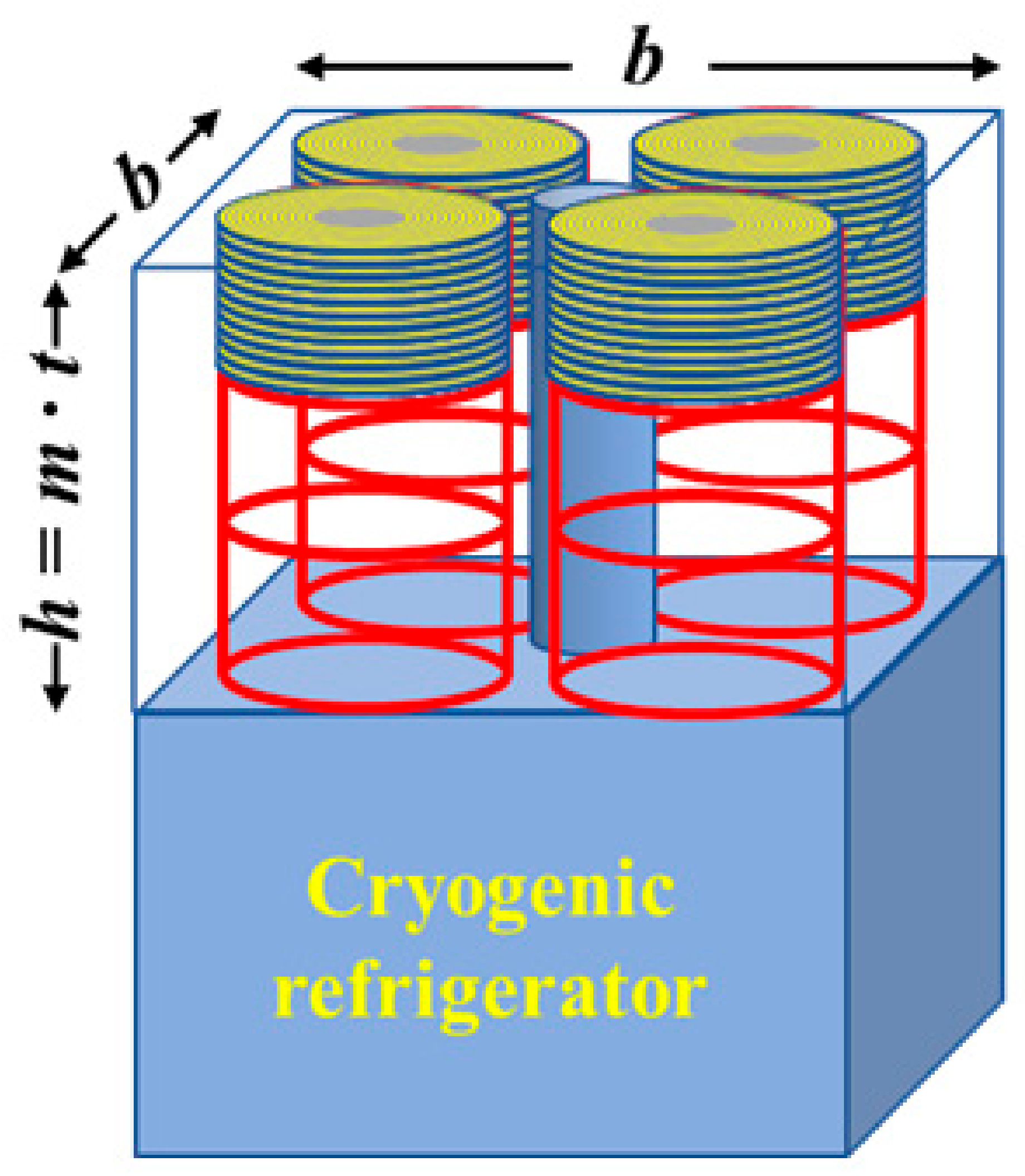
1.2. A Novel Approach to Increase the w and Mass Producibility of SMES

To increase the w of SMES from a sub-Wh/L level to a sub−10 Wh/L level ranking with the w of capacitors or more, we proposed the concept of a compact SMES, as shown in Figure 1. Without winding the superconducting cables or tapes at a small curvature radius, a superconducting thin-film coil is deposited and embedded in a spiral trench to prevent it from coming off from the substrate by electromagnetic stress S, which is applied to the coil, as shown in Figure 1a. Because S is a hoop stress put upon the outer wall of the trench, the superconducting current must be reduced to keep S lower than 1/3 of the mechanical strength limit of the Si wafer σSi: 4 GPa. Here, 1/3 is a safety factor. Multiple Si wafers, which are engraved with a spiral coil (hereafter, we call it a wafer coil for simplicity), are stacked and series-interconnected via through-holes based on 3D integration technology to form a cylindrical coil unit, as shown in Figure 1b [17]. In a typical possible concept design, the four units together with a compact cryogenic refrigerator are combined to form a typical possible minimum system, as shown in Figure 1c. Compact cryogenic refrigerators have been greatly improved recently and are on the market [18]. Here, the cryogenic refrigerator is drawn as a simplified form composed of a cuboid of b × b × h and a cylindrical tower with a height of h.

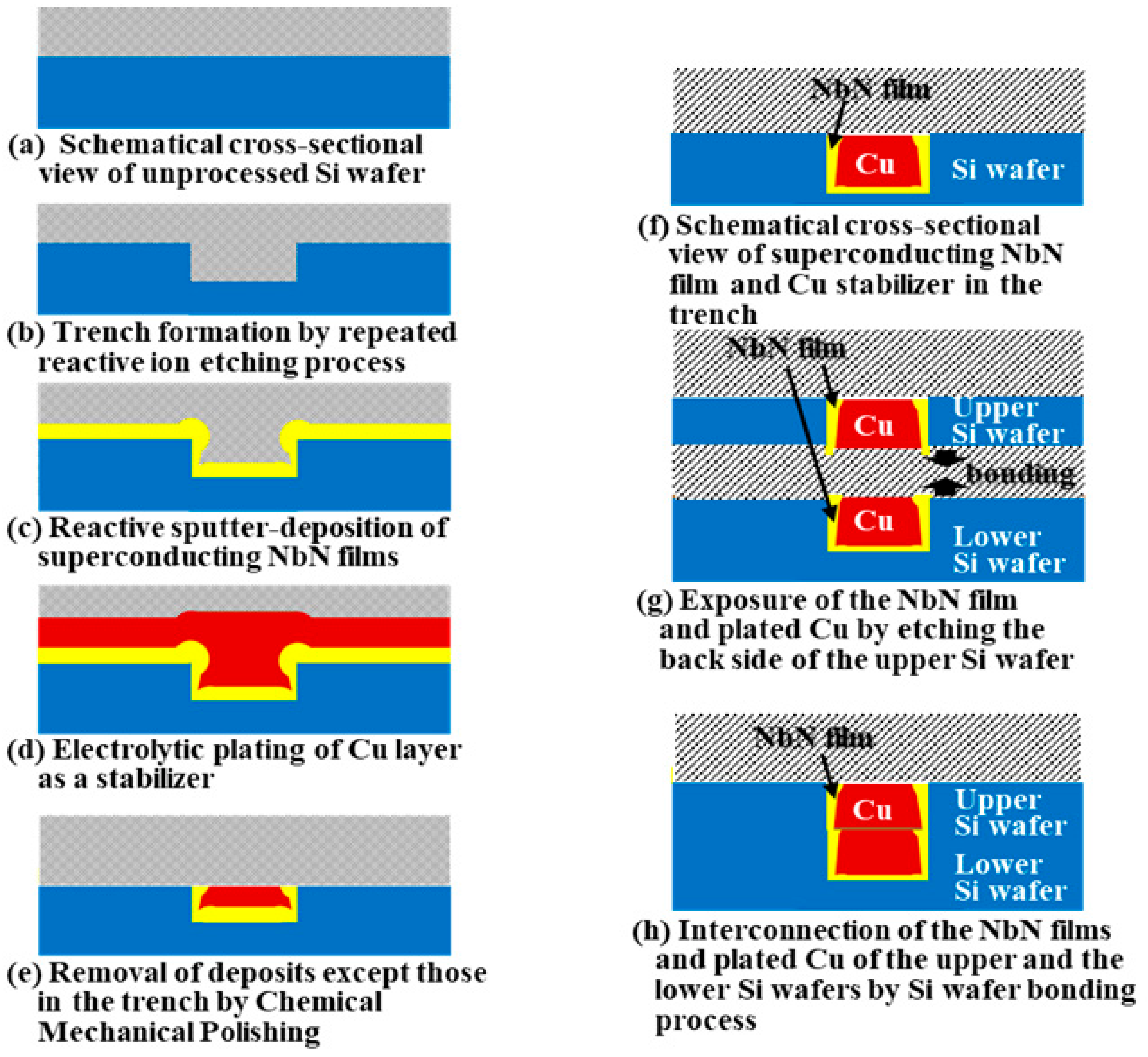
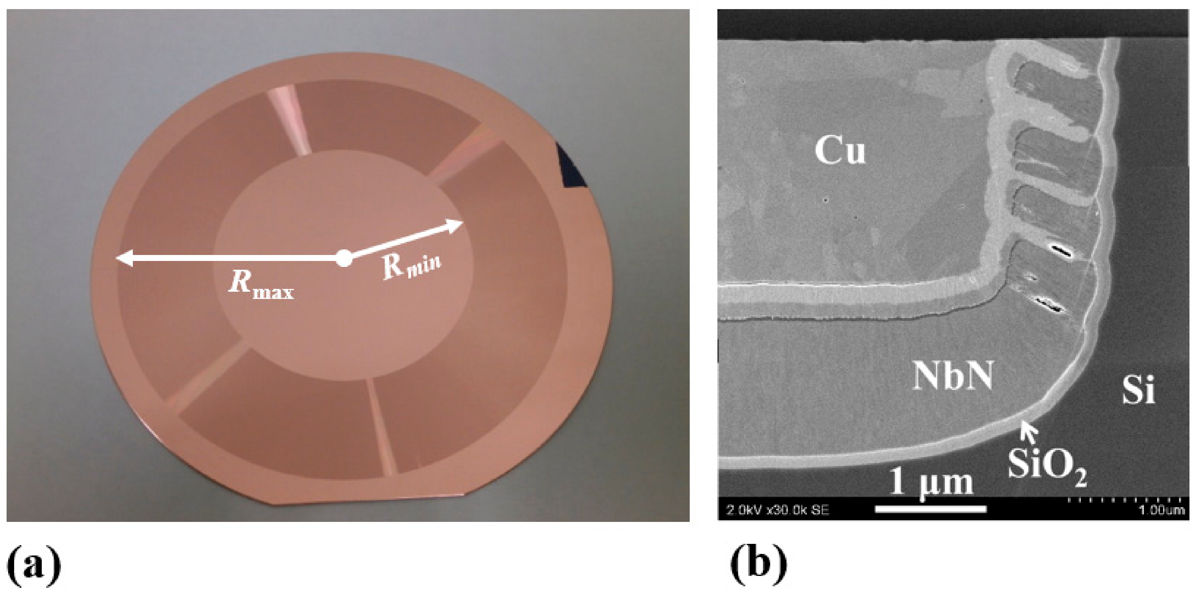
1.3. Experimental Proof of Concept Using Superconducting NbN Thin Films

A proof-of-concept experiment was performed on a single Si wafer using reactively sputter-deposited NbN superconducting thin films [19] and an electrolytically plated Cu layer as a stabilizer. Figure 2a–e schematically displays the process of trench formation; deposition of NbN and Cu; and the removal of unnecessary deposits of NbN and Cu, except for those in the trench, by chemical-mechanical polishing (CMP) step by step. Figure 2f–h schematically displays an example of the wafer bonding and series interconnection processes. Details of these processes were described in our previous report [20,21]. Figure 3a,b shows two photos of the Si wafer coils in a preliminary fabrication, corresponding to the process steps shown in Figure 2d,e, respectively. These process technologies were used to fabricate normal conductive MEMS (microelectromechanical system) inductors on Si wafers [22]. The measurement of the current–voltage characteristics in cryogenic temperatures together with the measurement of magnetic field by a gauss meter showed an energy storage of 0.01 mJ [20]. Increasing the NbN thickness by mitigating the film stress [23], the stored energy increased up to 0.1 mJ [24]. Here, the experimentally obtained jc of NbN—1100 A/mm2— was used [19]. The largest S near the central axis of the coil unit, Smax, estimated from the magnetic flux density B along the central axis of a single-layer solenoid was 0.11 GPa, which was well below σSi/3 [20,24].

1.4. Replacement of NbN by YBa2Cu3O7-δ to Increase Electricity Storage Volume Density

For further improvement, we moved on to the replacement of the reactively sputter-deposited NbN thin film by Y123 deposited by the metal-organic deposition (MOD) method [25,26,27]. Because metal-organic precursors dissolved in a carrier fluid such as propionic acid can easily go into the trench, this is advantageous in comparison with sputter deposition with a limited throwing power. Because the superconducting transition temperature (Tc) of Y123 is 90 K, this replacement enables the use of liquid hydrogen at 20.3 K or even of liquid nitrogen at 77 K as a refrigerant instead of a cryogenic refrigerator to cool below 13 K in the case of NbN. However, the real benefit of this replacement for SMES is that the jc of Y123 can be much higher than that of NbN if we keep using a 4 K cryogenic refrigerator.Figure 4 displays two curves, (a) and (b), of the measured jc of the c-axis-oriented Y123 thin-film tape at 4 K as a function of the magnetic flux density applied in parallel with the c-axis (redrawn from the literature [28,29,30]). According to curve (a), jc was measured to be up to 31 T in the applied magnetic flux density. There is no indication of a rapid decrease in jc due to the accession of the critical magnetic flux density Bc. It was also reported that Bc was also measured to be as high as 120 T at 4 K and continuously decreased with the temperature to 0 T at the critical temperature: Tc = 90 K [31]. Curve (b) shows more modest values of jc than the curve (a). Although the reported measured maximum applied magnetic field density was around 18 T in curve (b), it will be reasonable to conjecture that curve (b) in Figure 4 can be smoothly extrapolated beyond 18 T to at least 50 T, as shown in curve (c). Typically, the values of jc for the applied magnetic field of 15 T on curves (a) and (b) are 5 × 10⁴ A/mm2 and 2 × 10⁴ A/mm2, which are about 45.5 times and 10 times of 1100 A/mm2 in the case of NbN, respectively. Because w is proportional to the square of the current, we may expect, in comparison to the case of NbN, a 45.5 × 45.5 = 2070, and 18 × 18 = 324 times larger w in the case of Y123 for curves (a) and (b), respectively. Here, it should be noted that the maximum magnetic flux density at the innermost trench, Bmax is proportional to the superconducting current I, and S is proportional to I2. This means that the maximum superconducting current Imax in the coil must be much reduced from the value derived from jc because of the limitation of Bc and S = σSi/3. We intuitively know that we can mitigate this large B and S applied to the innermost portion of the coil by making the radius of the inner wall of the innermost trench, Rmin, larger, leaving the central part of the wafer uncovered with trenches, as shown in Figure 3a. However, we lose w simultaneously. Therefore, we must estimate how much we could mitigate B and S at the innermost portion of the coil and how much we lose w quantitatively in concrete designs of the wafer coils.

1.5. Aim of This Work

In our previous papers [32,33], we reported our series of trial estimations on this subject under the fixed jc of 2 × 10⁴ A/mm2. This value corresponds to a jc at 15 T on line (b) in Figure 4. However, jc is dependent on Bmax, as shown in curves (b) and (c) in Figure 4. There is also experimental evidence of higher jc, as shown in curve (a) in Figure 4. To make a more realistic estimation, the Bmax dependences of jc based on the two different jcBmax curves shown in Figure 4 were taken into consideration for the first time in our series of trial estimations. There was another item to refine the estimation. In the previous papers, the inductance L of the cylindrical coil unit made of the stack of series-interconnected wafer coils was calculated as an equivalent single-solenoid coil, which generated the same magnetic field intensity at the center of the coil. As for the radius of the equivalent single-solenoid coil, we simply used a mean radius a’ of Rmin and the radius of the outer wall of the outermost trench of the wafer coil, Rmax—that is, a’ = (Rmax + Rmin)/2. More precisely, the effective radius of the equivalent single-solenoid coil, a, should be smaller than a’ because the contribution of an inner coil to the magnetic field at the center of the wafer coil is larger than that of an outer coil. In this work, the effective radius a was also taken into consideration for the first time in our series of trial estimations. The aim of this work is to elucidate whether or not it is possible for SMES to increase w to rank with and to surpass the w of capacitors by the improved estimations. Tentatively, we started with the more modest curve (b) for the magnetic flux density dependence of jc.

2. Method of Estimation

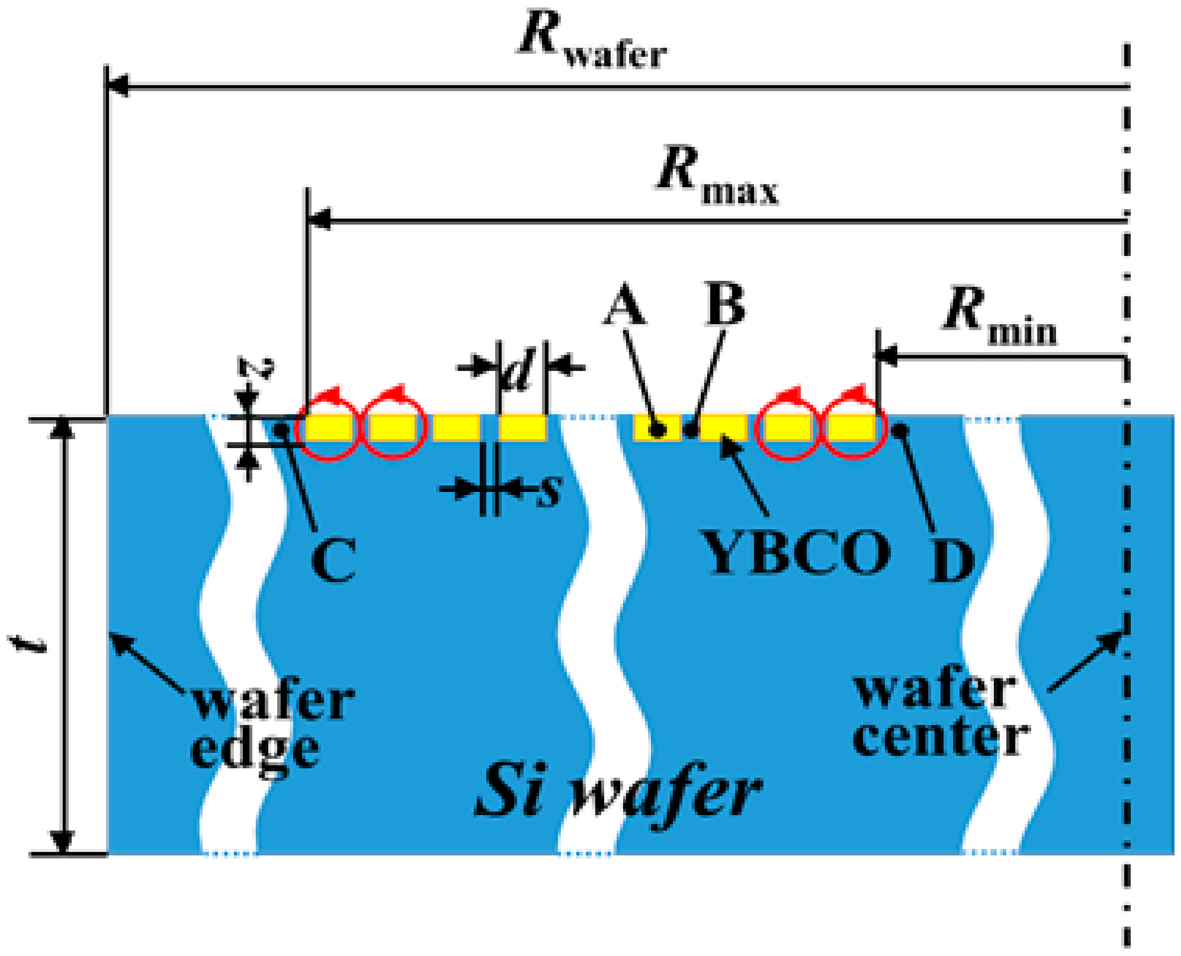
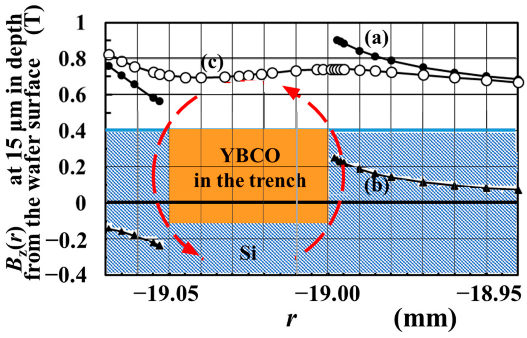
2.1. Calculation of Magnetic Flux Density in a Wafer Coil

Figure 5 schematically illustrates approximately one-half of the cross-section of a wafer coil, showing the principal design parameters of the spiral trench. Here, Rwafer and t stand for the radius and thickness of the Si wafer, respectively. Parameters d, z, and s stand for the trench width, trench depth, and trench wall thickness, respectively. The yellow rectangles indicate cross-sections of the trenches filled with Y123. Here, the trenches are supposed to be filled with Y123 and the presence of stabilizer layers as shown in Figure 2 and Figure 3b is neglected for simplicity. The red circle with an arrow around a trench schematically indicates a typical magnetic field generated by the currents flowing Y123 in the trench from the back to the surface of the plane of paper.
As for the calculation of the distribution of magnetic flux density in the wafer coil, we replaced a spiral coil with the number of turns n by n conductive concentric circular current paths with the same Rmax, Rmin, d, s, and z for a calculation model. In all the n concentric current paths, the currents were supposed to be the same. The calculation was based on the Biot-Savart law, as shown in the following equation in SI units:
B r = μ 0 4 π I d q r r 3
Here, μ0 is the magnetic permeability of free space: 4π × 10−7 H/m. I is the absolute value of the current in the circular current path. B(r) is the vector for magnetic flux density at the position defined by vector r. The wire element dq is the vector of the circular current path element whose magnitude is the length of the differential element of the circular current path in the direction of the current at the position defined by vector q. The vector r =rq is the full displacement vector from dq d ℓ {\displaystyle d{\boldsymbol {\ell}}}at point q ℓ {\displaystyle {\boldsymbol {\ell}}} to point r. The expression dqr represents the cross product of the vectors dq and r. Numerical calculation was performed by integrating current density jc in the d by z rectangular cross-section of the trench using the “integ.tplquad” function in a Python 3.6 calculation code.r {\displaystyle \mathbf {r}} The calculated magnetic flux density using this calculation code at the center of a single circular current normal to the plane of the circle was confirmed to agree with the value obtained from the analytical expression (4) deduced from Equation (3):
B z = μ 0 I 2 a 1
where a1 is the radius of the circular current I. B(r) in the trench in which r can be equal to q cannot be calculated by Equation (3) because the integrand containing r’ = rq in its denominator reaches an infinite value. Typical calculations of B(r) for a single planar spiral coil formed in a spiral trench of width: d = 50 μm; depth: z = 30 μm; the trench wall thickness: s = 22 μm; Rmin = 19 mm; and turn number n: 400 (resulting in Rmax = 47.8 mm on a Si wafer of the diameter 2Rwafer = 101.6 mm) were performed assuming a fixed jc of 2 × 10⁴ A/mm2. In the actual calculation by this calculation code, the B(r)s caused by concentric 400 circular currents were summed up as a model of the single planer spiral coil. Figure 6a shows the results of the calculations of the radial distribution of the magnetic flux density normal to the wafer coil, Bz(r), at the half depth of the trench. Here, the scalar: r is the absolute value of the vector r when the origin of r and q is located at the center of the wafer plane. The calculation of Bz(r) when r is located out of the trench can be performed because r’ in the denominator of the integrand in Equation (3) cannot be zero. Here, let us call this type of calculation Type I. The solid black circles stand for the calculated Bz(r) of Type I. We need to know Bz(r) penetrating the Y123 in the trench to estimate the electromagnetic hoop stress imposed on the Y123 as well as the jc under the magnetic field generated by the other parts of the concentric circular currents. Because the magnetic flux generated by the current in a portion of a trench does not penetrate the same portion of the trench, the current in the corresponding portion can be eliminated from the estimation of Bz(r). Accordingly, the calculation of Bz(r) in the trench was also performed by eliminating the current element in a small volume portion of the trench surrounding the calculating positionr from the integral shown in Equation (3) so that r does not become equal to q. Let us call this type of calculation Type II. The open black circles in Figure 6a indicate the Bz(r) calculated in the trench by Type II. The small volume portion was defined as the volume portion in the circular trench within the plane angle area ±δ in the vicinity of the point r subtended at the center of the Si wafer. Figure 6b schematically display the small volume portion of a trench surrounding a calculated position indicated by A employed in the calculation of Type II in a special case where the trench is the inner-most circular trench. As for the concrete value of δ in Type II calculations, 0.001 radian was employed. In this sense, the calculation of Type I can be regarded as the calculation of Type II at δ = 0, as shown in Figure 6a. In this special case of the Type II calculation, several values of Bz(r) for r < Rmin, out of the trench, were also calculated at the several points including r = 0 mm and plotted with open black circles in Figure 6a. In the region r < Rmin, the points calculated by Type I and Type II are on the same line. Thus, it is duly elucidated that the effect of the elimination of the current in the volume portion of the innermost circular trench on Bz(r) in this area, r < Rmin, was negligible. When r approached Rmin in the area r < Rmin at the position D shown in Figure 5, Bz(r) steeply increased in the Type I calculation. Figure 7 displays the calculated values of Bz(r) more in detail than Figure 6a in the vicinity of the innermost trench. Type I calculations were only performed for the positions out of the trench, as plotted with the solid black circles (a), while Type II calculations were performed also in the trench, as plotted with the open black circles (c). Type I calculations for a single innermost circular trench without the other concentric trenches were also conducted and plotted with solid black triangles (b). It is obviously known that the increase in (a) when r decreased and approached Rmin = −19.00 mm was caused by the contribution of (b). In the Type II calculation, Bz(r) takes a smaller value of 0.71 T at position A (r = 19.025 mm) in the center of the trench in Figure 6b in comparison with 0.84 T by the Type I calculation at r = 18.99 mm. In the peripheral area near the edge of the Si wafer, as indicated with C in Figure 5, the values indicated with the solid black circles in Figure 6a steeply decrease with the distance from the wafer center, in contrast to the open black circles staying near the zero magnetic field line in the same figure. This is because the magnetic flux density produced by the outermost ring current gives negative Bz(r) at the position C, while this does not take place in Type II calculation. Except for this difference, the calculated values for Bz(r) generally showed a decrease with the increase in r for both the solid black circles and the open black circles in Figure 6a. As shown in Figure 6a, Bz(r) takes the highest value in the innermost trench in a wafer coil.

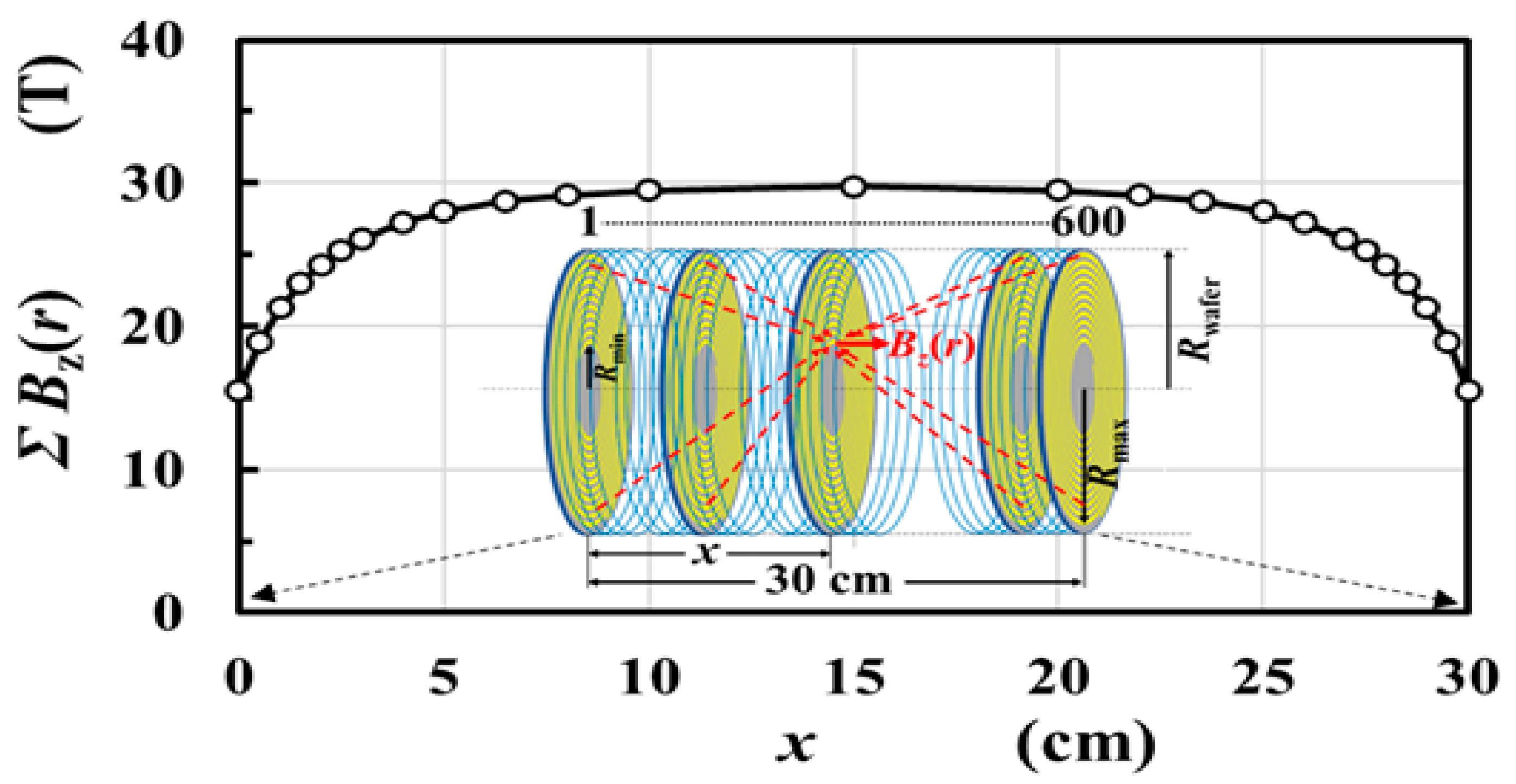
2.2. Calculation of Magnetic Flux Density in a Stack of Wafer Coils

In the case of the cylindrical unit of the stacked wafer coils, the magnetic flux density caused by a different wafer coil in the stack is also imposed on the innermost trench in question. Figure 8a schematically illustrates the component of the magnetic flux density Bz(r) normal to the wafer at the innermost portion of the spiral coil at the radius Rmin + d/2 and at depth z/2 in a wafer caused by another wafer coil at a distance x in the same stack with a red arrow. If the sum of contributions of magnetic flux densities caused by all the stacked wafer coils at a position in the innermost trench of a wafer coil exceeds jc, the current density must be reduced to maintain superconductivity. The radial outward-directed black arrow indicates the electromagnetic hoop stress imposed on the inner-most trench by the accumulated magnetic flux density of the all the contributions from the stacked wafer coils shown in the red arrows. Figure 8b shows the dependence of Bz(r) on x when Rmax = 47.8 mm, Rmin = 19.0 mm, d = 50 μm, s = 22 μm, z = 30 μm, and t = 0.5 mm. Because Bz(r) is plotted in logarithmic scale, it is clearly shown that Bz(r) decreases rapidly with increasing x, and it is lower than 10% of the peak value when x > 2.5 cm. The sum of the contributions Bz(r) of all the wafers in a stack is denoted by ΣBz(r). Figure 9 displays a variation in ΣBz(r) as a function of the position of the wafer x in the stack in a typical case of the height of the cylindrical coil unit: m = 600. Although ΣBz(r) has a maximum at x = 15 cm, it is almost constant, except for the regions near x = 0 cm and x = 30 cm. This is because the major contributions of Bz(r) are of wafer coils at x < 2.5 cm, as shown in Figure 8b. Figure 10a displays the dependence of the ΣBz(r)-x curve on Rmin. The maximum value of ΣBz(r) at x = 15 cm, Bmax,almost linearly decreased with Rmin, as shown in Figure 10b.

2.3. Calculation of Inductance of the Wafer Coil Stack

Bz(0)—i.e., Bz(r) at r = 0.0 mm—was calculated as a function of Rmin, as shown in Figure 11. Here, the Type I calculations were employed because r = 0.0 mm represents the center of the wafer, which is located out of the trenches. The radius a of a single circular current: ndzjc, which yields the same magnetic flux density as Bz(0) at its center is calculated by Equation (4) and also plotted as a function of Rmin in Figure 11. It is shown that a is generally smaller than the mean radius of the spiral coil a’ = (Rmax + Rmin)/2, and this deviation increases with a decrease in Rmin.
The m wafer coils are supposed to be stacked to form a cylindrical unit of 2Rwafer in diameter and mt in height. The spiral coils on adjacent Si wafers are supposed to be series-interconnected through two through-holes [17,20] formed in the wafers by such a method illustrated in Figure 2f–h, which is frequently used in conventional multi-layer interconnection technology for 3D integration [17]. Thus, the series-interconnected stacked multiple wafer coils form a combined coil of inductance L. For simplicity in the calculation of inductance, L, these series-interconnected wafer coils were simulated to be a single-layer solenoid of the length mt and of the equivalent radius a given in Figure 11. If the number of turns of the coil in a wafer is n, L can be expressed using the formula for the single-layer solenoid as follows:
L = K μ 0 μ r π a 2 n m 2 m t
where K is Nagaoka’s coefficient, which is a function of a/(mt), μr stands for relative magnetic permeability. In the case of Si, it is reasonable to set μr = 1. Figure 12 displays the calculated values of L as a function of Rmin in the case where the equivalent radius a shown in Figure 11 was employed for the equivalent single-layer solenoid. The calculated values of L in the case where the mean radius of the spiral coil a’ = (Rmax + Rmin)/2 were employed for the equivalent single-layer solenoid, are also displayed for comparison. It was found that L took the maximum value around Rmin = 13 mm when the equivalent radius, a, was employed, while L showed no peak when the mean radius, a’, was employed. The appearance of the maximum was caused by the variation in the product, a × n, in Equation (5), where a increased rapidly with Rmin and n decreased rapidly with Rmin. In contrast, the linear increase in a’ with Rmin did not cause a maximum in variation of the product a’ × n in Equation (5).

2.4. Calculation of Electricity Storage Volume Density of the Wafer Coil Stack

The electric energy E stored in a solenoid of inductance L can be expressed as:
E = 1 2 L I 2
Here, the superconducting current I, which flows in the coil at the critical current density jc can be expressed as I = dzjc. Here, w is calculated for the volume of cuboid including 4 stacks, as shown in Figure 1c—that is, in the special case of l = mt. Because the volume of the cuboid in Figure 1c is b × b × 2h, including the space for refrigerant, magnetic shields, heat insulation, and cryogenic refrigerator, w = E × 4/(b × b × 2h). Here, another volume of b × b × h is supposed to be necessary for the cryogenic refrigerator in addition to the upper container of the volume of b × b × h for 4 cylindrical wafer stack units. In this paper, estimations of w were performed for the cases of b = 0.3 m and t = 0.5 mm. The value n can be expressed as n = (Rmax + s Rmin)/(d + s). Because s/Rmax ≪ 1 and s/Rmin ≪ 1, n can be approximated as follows:
n = R max R min d + s
Then, (5) can be expressed as follows:
L = K μ 0 π a 2 R max R min d + s m 2 m t
Then, w can be expressed as follows:
w = 1 2 K μ 0 π a 2 R max R min d + s m 2 m t d z j c 2 × 4 b × b × 2 h = 2 K μ 0 π a 2 R max 2 1 R min R max 2 1 1 + s d 2 z j c 2 b × b × 2 h t / m
Because trenches cannot be formed on the peripheral ring area of the Si wafer with a width of at least 3 mm for the handling of the wafer in the series of processes, Rmax can be set in a limited range and is essentially constant. Therefore, w increases with a decreasing Rmin. Equation (9) also teaches us that w increases with a decreasing (s/d) and with increasing z. Because h = mt in the special case drawn in Figure 1c, the denominator of Equation (9) does not contain the number of Si wafer coils, m. However, an increase in m can contribute an increase in w, because K increases with m∙t/a. A decrease in a with a decrease in Rmin, as shown in Figure 11, can also contribute to an increase in w via an increase in K. However, w increases with a because Equation (9) contains a2 in the numerator. Therefore, w can increase with an increasing Rmin. Thus, it is not straightforward to know the actual variation in w.

2.5. Electromagnetic Hoop Stress

Expressing free electron density as ρ m−3 and elementary charge 1.60 × 10⁻⁷ C as e, the charge q C in the superconducting film per length dx along the trench can be expressed as q = eρdzdx. Expressing the electron velocity as v, I is expressed as I = eρdzv. The Lorenz force F imposed on the current I can be expressed as F = qvB = I∙dxΣBz(r). Because the corresponding surface area on the trench wall is z∙dx, the hoop stress S in the unit of GPa on the trench wall can be expressed as follows:
S = I d x B z r z d x × 10 9
Because S is normal to B and I, S gives the hoop stress, as shown in Figure 8a. When ΣBz(r) takes the maximum value ΣBmax at the innermost trench, S also takes the maximum value, Smax. Figure 13 displays the variations in the electricity storage volume density, w, Smax, and ΣBmax, as a function of Rmin.

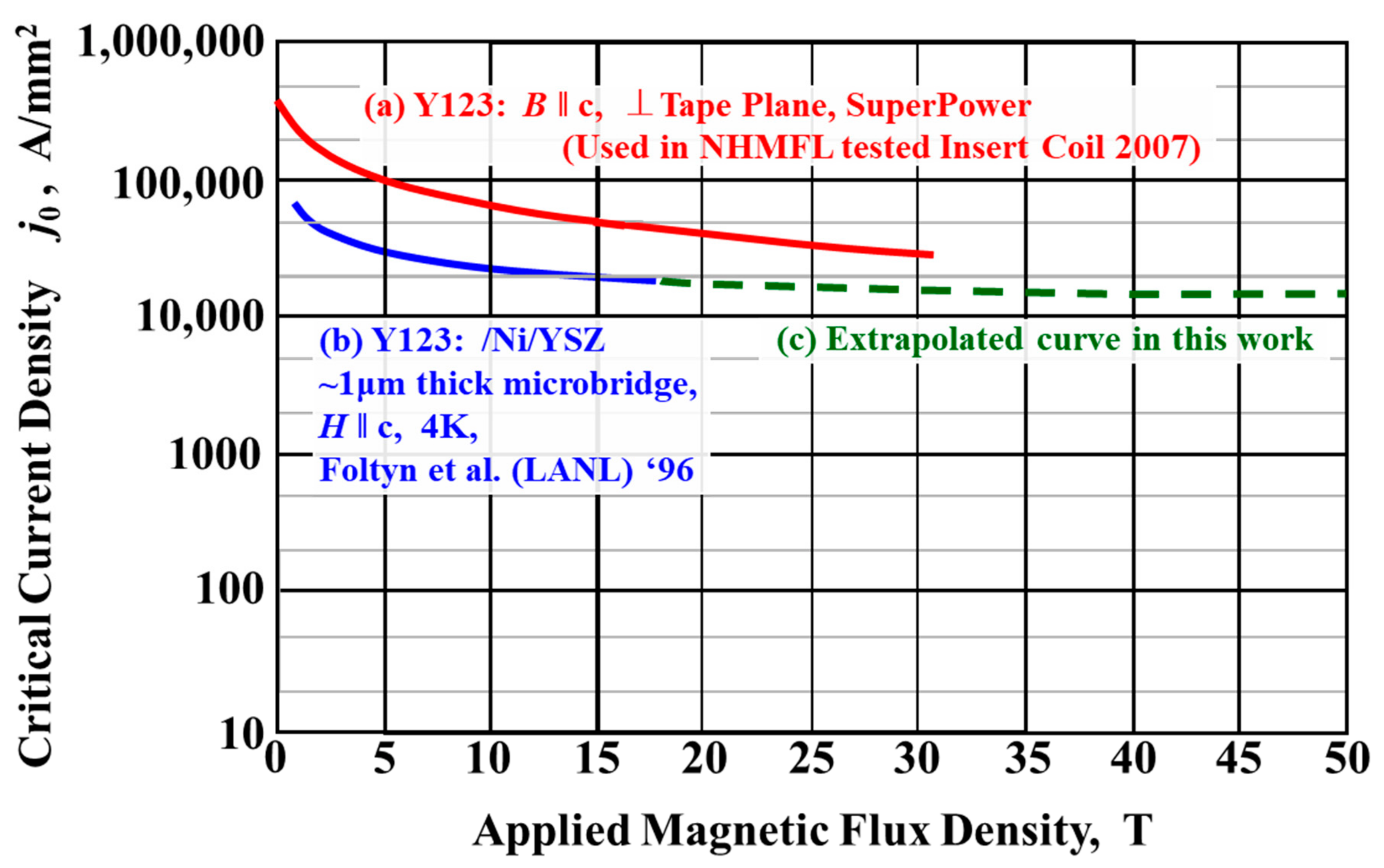
2.6. Consideration of Magnertic Flux Density Dependent jc in the Calculation

The results displayed in Figure 13 were calculated using the magnetic flux density independent jc of 2 × 10⁴ A/mm2. In the next step, the magnetic flux density dependent jc shown in curves (b) and (c) in Figure 4 is taken into consideration. This is essentially an iteration process in which the Σmax decided by the initially set value jc0 reduces jc0 to jc1, and then jc1 decides the new value of ΣBmax1, which reduces jc1 to jc2, and so on. For the convenience of calculation, jc was expressed as a function of ΣBmax in expression (11) based on curves (b) and (c) in Figure 4.
j c A / m m 2 = 85,800 B max T + 0.672 + 12,900
This iteration process finally gave converged values of jc∞ and ΣBmax∞. Figure 14 displays the w and Smax obtained with Equations (9) and (10) using j c∞ and ΣBmax∞ as functions of Rmin. It is found that w and Smax were much reduced in comparison with Figure 13. The perpendicular dashed-dotted red line was drawn to show the value of Rmin at which ΣBmax took the value of 20 T. The red open circle indicates that the ΣBmaxRmin curve crosses the line of ΣBmax = 20 T. The corresponding value of Rmin was 24.7 mm. If superconductivity is retained up to this ΣBmax: 20 T, it is shown that the value of w: 3.6 Wh/L is attained at Rmin: 24.7 mm where Smax takes the value of 0.017 GPa. The perpendicular dashed-two dotted blue line was drawn at the value of Rmin at which w took the maximum value of 4.3 Wh/L. The corresponding value of Rmin was 15.3 mm, where ΣBmax and Smax took the values of 26.7 T and 0.021 GPa, respectively. Therefore, it was shown that the value of w, 4.3 Wh/L could be attained if the wafer coils are superconductive up to ΣBmax = 26.7 T. Here, it should be noted that the equivalent radius a does not change with the reduced critical current Ic because Bz(0) is also reduced in proportion to the reduced Ic = ndzjc, and the ratio I/Bz(0) does not change in Equation (4).

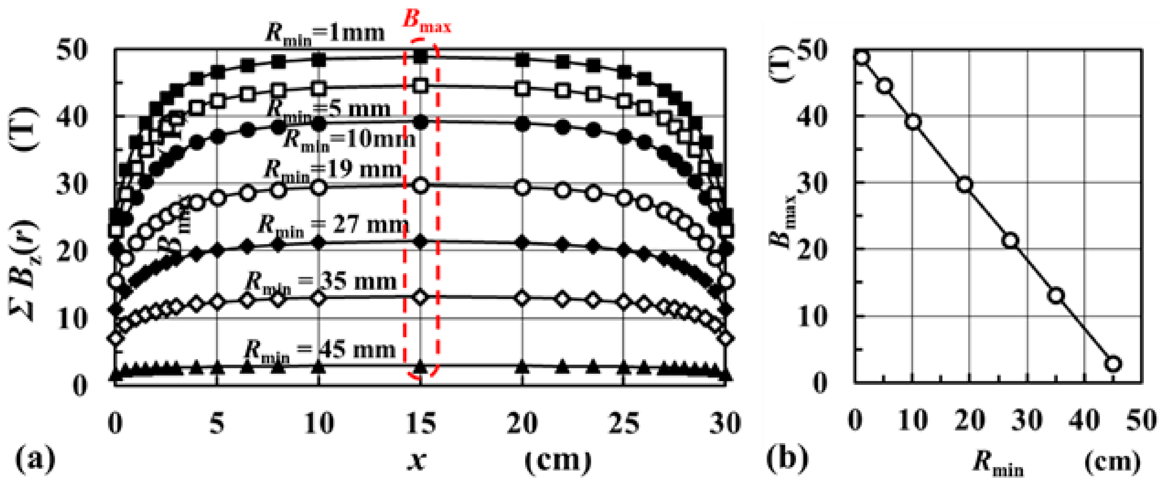
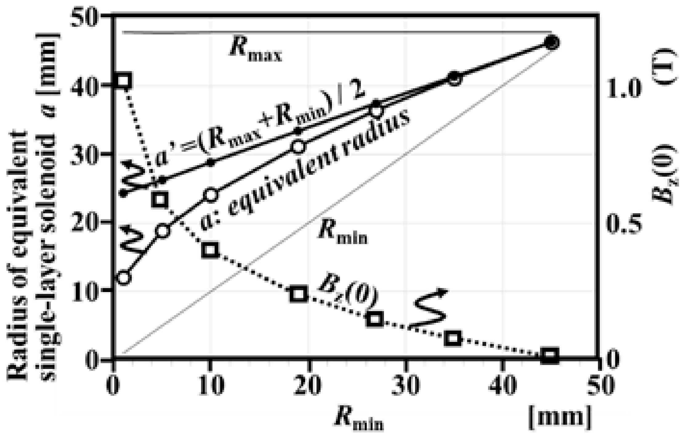
2.7. Effects of the Wafer Coil Design and the Hight of the Wafer Coil Stack on the Electricity Storage Volume Density

The results shown in Figure 14 were obtained for the Si wafer with radius Rwafer = 50.8 mm, the radius of the outer wall of the outermost trench Rmax = 47.8 mm, and the thickness t = 0.5 mm in the case of the trench width d = 50 μm, the trench wall thickness s = 22 μm, the trench depth z = 30 μm, and the number of stacked Si wafers m = 600. Here, the effects of changing d, s, z, and m in practically viable ranges on ΣBmax, w, and Smax were examined.
As mentioned above, Equation (9) teaches us that w increases with decreasing (s/d) and with increasing z. Because w does not depend on the absolute values of d and s but depends on the ratio s/d, the examination of the different values of the sum d + s is not necessary. Therefore, the cases of d = 70 μm and s = 2 μm were examined at the same sum d + s in the case of d = 50 μm and s = 22 μm. As was elucidated in Figure 8b and Figure 9, the contributions of the stacked wafers at a distance more than 5 cm to ΣBz(r) are negligible. The distance of 5 cm in the stack corresponds to 100 wafer coils. Therefore, cases of m = 200 in addition to cases of m = 600 were examined. Although the change in m from 600 to 200 decreases L, as shown in Figure 15, and hence the amount of the magnetic energy storage for each cylindrical coil decreases, eight more cylindrical coil units can be installed in the cryogenic container of the volume b × b × h, as shown in Figure 16, which in turn increases w. Although w increases with an increasing z, there is an experimental limitation in increasing z because of the following reasons. The high-temperature heat treatment of the wafer coil in an oxygen atmosphere is indispensable for the crystallization and adjustment of oxygen deficiency δ in YBa2Cu3O7-δ. This heat treatment induces the diffusion of Si into the Y123 layer, which degrades the superconducting property of Y123. To prevent this, some intermediate buffer layers are necessary between Si substrates and Y123 layers. The buffer layers are also necessary to mitigate lattice and thermal expansion coefficient mismatches between Y123 and Si. For these reasons, the sputter deposition of the yttria-stabilized zirconia layer succeeded by the sputter deposition of the CeO2 layer was used to form the intermediate buffer layers [34,35], and we also employed these buffer layers in our previous experimental study [27]. Because the throwing power of sputter deposition into the trench is limited, the large aspect ratio of the trench, z/d, cannot be employed. Therefore, cases of z = 100 μm were examined as a realistic value in addition to cases of z = 30 μm. Figure 17 schematically summarizes the combinations of the wafer coil design parameters, d, s, z, examined here.

2.8. Comparison of the Effects of the Wafer Coil Design and the Height of the Wafer Coil Stack under Two Different Magnetic Flux Density-Dependent jc

Like Equation (11) for curves (b) and (c) in Figure 4, jc was also expressed as a function of ΣBmax based on curve (a) in the following expression (12):
j c A / m m 2 = 59,400 B max T + 1.75 + 9630
Iteration processes using Equation (11) or Equation (12) gave converging values of jc∞. and ΣBmax∞ as a function of Rmin. Then, jc∞. and ΣBmax∞ gave w and Smax as a function of Rmin.

3. Results

The results of the calculations of ΣBmax, w, and Smax as a function of Rmin for two different value settings of m, d, s, and z shown in Figure 16 and Figure 17 are displayed in the same manner as in Figure 14; in Figures S1–S4 in the case of the magnetic flux density-dependent jc of curves (b) and (c) in Figure 4, which is simulated by Equation (11); and in Figures S5–S8 in the case of the magnetic flux density-dependent jc of curve (a) in Figure 4, which is simulated by Equation (12), respectively. The values of w, Rmin, Smax, and ΣBmax indicated by the perpendicular dashed-dotted red lines and the perpendicular dashed-two dotted blue lines in Figures S1–S8 are summarized in Table 1. In Table 1, w @20T and w peak stand for w at ΣBmax = 20 T and the peak values of w, respectively. In the case of the ΣBz(r) dependence of jc expressed by Equation (11) (curves (b) and (c) in Figure 4), w@20T took values between 3.5 and 4.5 Wh/L in the range of Rmin 21.5–31.4 mm when z = 30 μm, while w@20T took values between 5 and 6.8 Wh/L in the range of Rmin 40–43.5 mm when z = 100 μm. An increase in d from 50 to 70 μm also caused an increase in w@20T and Rmin. The difference in m between that illustrated in Figure 1c and in Figure 16 did not cause simple trends of increase nor decrease in w@20T but caused a slight decrease in Rmin with decreasing m.
In the case of the ΣBz(r) dependence of jc expressed by Equation (12) (curve (a) in Figure 4), w@20T took values between 5.1 and 5.6 Wh/L in the range of Rmin 34.9–40.3 mm when z = 30 μm, while w@20T took the values between 6.1 and 6.7 Wh/L in the range of Rmin 43.7–45.8 mm when z = 100 μm. An increase in d from 50 to 70 μm caused an increase in Rmin but did not cause an increase in w@20T. A decrease in m from 600 to 200 caused a slight increase in w20T and slight decrease in Rmin.
In the case of the ΣBz(r) dependence of jc expressed by Equation (11) (curves (b) and (c) in Figure 4), wpeak took values between 3.9 and 7.6 Wh/L in the range of Rmin 13.5–13.9 mm when z = 30 μm, while wpeak took values between 33.8 and 69.4 Wh/L in the range of Rmin 40–43.5 mm when z = 100 μm. An increase in d from 50 to 70 μm also caused an increase in wpeak. A decrease in m from 600 to 200 caused a decrease in wpeak.
In the case of the ΣBz(r) dependence of jc expressed by Equation (12) (curve (a) in Figure 4), wpeak took values between 9.3 and 14.9 Wh/L in the range of Rmin 18.8–19.4 mm when z = 30 μm, while wpeak took values between 48.2 and 80 Wh/L in the range of Rmin 16.6–17.5 mm when z = 100 μm. An increase in d from 50 to 70 μm caused an increase in wpeak but did not cause an increase in Rmin. A decrease in m from 600 to 200 caused a decrease in wpeak.
Although the values of wpeak often exceeded 10 Wh/L and sometimes approached 100 Wh/L when z = 100 μm or d = 70 μm, the corresponding values of ΣBmax often exceeded 50 T and 100 T in some cases. These large values of ΣBmax may exceed the critical magnetic flux density, although there are no signs of the appearance of critical magnetic flux density within the range shown in Figure 4. Table 2 lists the values of w taken from Figures S1–S8 at the ΣBmax of every 10 T increment up to wpeak.
Table 2 shows that the values of w@20T at ΣBmax = 20 T are lower than 10 Wh/L in all the different wafer coil design parameters, d, s, z, and the number of stacked wafer coils m under the different ΣBmax dependences of jc. In the cases of z = 100 μm and in some cases of d = 70 μm, the values of w at ΣBmax are higher than 20 T and can be larger than 10 Wh/L, or more with an increase in ΣBmax. It is found that this trend is more enhanced in the case of the ΣBz(r) dependence of jc expressed by Equation (12) (curves (a) in Figure 4) than in the case of the ΣBz(r) dependence of jc expressed by Equation (11) (curves (b) and (c) in Figure 4). In all conditions, the values of Smax were found to take values well below 1/3 of the mechanical strength limit of the Si wafer σSi: 4 GPa.

4. Discussion

4.1. Possibility of SMES to Rank with or Surpass Capacitors in Electricity Storage Volume Density

The dependence of jc of Y123 thin films on the magnetic flux density is sensitively affected by many experimental factors such as the methods of deposition, deposition conditions, substrates, buffer layers, etc. The data displayed in Figure 4 are the dependences of jc on magnetic flux density in parallel with the c-axis of preferentially c-axis-oriented Y123 thin films. Y123 thin films sometimes grow in mixed orientations of the c-axis and a-axis [25,27]. Even if c-axis-oriented Y123 is successfully grown on buffered Si substrate [26], the c-axis of the Y123 thin film grown on the bottom of the trench and the c-axis of the Y123 thin film grown on the trench wall cannot be in parallel with the same magnetic flux simultaneously. Therefore, there remains many challenges in material science and engineering to attain depositions of high-quality Y123 thin films with a sufficient magnetic flux density dependence of jc in the trench. However, the existence of the experimental evidence shown in Figure 4 encourages us to develop a compact SMES with the new concept presented in this work, which can rank with or surpass the capacitors on the market in terms of electricity storage volume density. The results summarized in Table 2 teach us that w can rank with the commercially available capacitors, including EDLC, if superconductivity is retained up to the magnetic flux density ΣBmax of 20 T. The results also teach us that w can surpass capacitors including EDLC if superconductivity is retained up to a ΣBmax of 30 T. According to the experimental evidence of curve (b) and (c) shown in Figure 4, superconductivity is retained up to ΣBmax = 18 T. It will be duly considered that superconductivity is retained up to 20 T. According to curve (a), superconductivity is retained up to a ΣBmax of 31 T. Moreover, there is a possibility that superconductivity is retained beyond 40 T, because there is no indication of a rapid decrease in jc due to the accession of the critical magnetic flux density Bc. In this case, w may rank with commercially available hybrid energy storage capacitors [4]. According to the results summarized in Table 2 for the different trench design parameters illustrated in Figure 17, there remains possibilities to attain a greater w by using deeper and wider trenches within the experimentally feasible ranges.

4.2. Improvement for Lower Cost and Compatibility for Mass Production

According to Table 1, a decrease in m from 600 to 200 accompanied by an increase in the number of wafer stacks from 4 to 12 as illustrated in Figure 16 caused no significant effect on w. This is good news because the process to stack 200 wafer coils is much easier than the process to stack 600 wafer coils from the viewpoint of a reduction in yield loss and process cost. The semiconductor microfabrication processes used here for the fabrication of the units of stacked wafer coils are compatible in nature with unattended automatic mass production and have the possibility to yield a significant cost reduction, which has been attained in the production of solar panels in which several tens of Si wafers are installed in one product (panel), just like the compact SMES proposed here. However, it is a great challenge to reduce the process cost of the repeated reactive etching process for trench formation and multiple wafer-bonding processes. In April 2018, the present authors noticed the announcement of the commercialization of a compact analyzer gas chromatograph, which is more than 30% smaller and gives 50% less analysis time compared with the conventional ones equipped with capillary columns [36]. The main part of this product is made of spiral trenches formed in a stainless steel substrate and stacked with another stainless steel plate as a lid in place of the capillary columns.
The development of this product started with the microfabrication of spiral trenches on Si wafers [37], just like the present study. According to the result summarized in Table 1, the values of the maximum hoop stress Smax induced on the trench wall were less than 0.2 GPa, which was well below the 1/3 mechanical strength limit of the Si wafer σSi, 4 GPa. This fact indicates that other substrate materials such as typical engineering ceramics or metals can be used in place of a Si wafer if an imprinting process or molding process for spiral trenches is feasible. Therefore, the compact SMES in the proposed concept may follow in the same footsteps of development of the compact analyzer gas chromatograph mentioned above. This possibility of the employment of substrate materials other than Si may also open the door to other applications of the present wafer coils besides SMES—such as, for example, magnetic resonators for wireless power transfer systems with a longer transfer range utilizing the high-quality factor of superconducting coils [38].

4.3. Applications of the Compact SMES Which Ranks with or Surpass the Commercially Available Capacitors

A SMES has been developed for a power system control such as load fluctuation compensation and power system stabilization [6,7,8,9,10,39]. However, those infrastructural applications have been proposed for usage in the space of a loosely restricted volume condition based on the electricity storage volume density of the sub-Wh/L level of conventional SMESs. Therefore, the benefit of the compact SMES proposed in the present study is limited. Of course, the compact SMES of the proposed concept may be distributed widely in the market by mass production and may contribute to these conventional applications at a lower cost and in a much reduced volume. Here, let us focus one of the outstanding features of the SMES: its rapid high-power delivery of around MW/msec. This feature makes the SMES suitable for pulsed power load operation [40]. An extreme example of a pulsed power load is a lightning strike. Controlling lightning strikes to prevent them from causing damage to various infrastructures and facilities is a serious task for telecom companies. Recently, there was an announcement that Nippon Telegraph and Telephone Corporation (NTT) started a study of technology to capture and guide lightning strikes [41]. In the project of NTT, it is planned that drones flying near the thunder clouds guide lightning electricity with the attached conductive wire to the ground in place of the kite used by Benjamin Franklin. In the project, it is also considered to guide the lightning electricity with the conductive wire to an electricity storage facility on board of a car. Reportedly, there is a wide variety of the properties of lightnings with their current from 1 kA to 200 kA, with their voltage from 2 MV to 200 MV, with their pulse width from sub-msec to 1 sec, and power from 10 kWh to 500 kWh. If we take the values of the most frequent occurrences, the electricity pulse of lightning is typically 25 kA, the voltage is typically 29 MV, the pulse width is typically 1 msec, and the power is typically 200 kWh. The pulse width is too narrow to charge rechargeable batteries. The corresponding voltage of 29 MV may be too high for conventional capacitors to be charged. As for SMES, a feasibility study for energy regeneration on-board ground vehicles has been reported, although the proposed system was still as large as about 1 m in diameter and heavy, with bulky reinforced structures against the hoop stress [16]. The total electricity of 200 kWh of one lightning requests the volume of 400 m3 if the typical conventional electricity storage volume density w of 0.5 Wh/L is employed. This is too large to install on-board a car. However, the compact SMES of the proposed concept in this work requests a volume of 40 m3 if w is 5 Wh/L. This compact SMES can be installed on-board a standard 4-ton truck. Although it goes without saying that SMES also requires improved insulation barriers and more detailed engineering efforts, this topic is mentioned here to elucidate the merit of the compact SMES of the proposed concept.

5. Conclusions

SMESs store electricity as the energy of a magnetic field in contrast to capacitors, which store electricity as the energy of an electric field. Because SMESs and capacitors store electricity based on purely physical phenomena, their abilities of rapid charge and discharge are specific to them in contrast to rechargeable batteries based on an electrochemical phenomenon. However, SMESs are heavy electric machinery products of a relatively high cost, which is caused by their made-to-order production, while varieties of capacitors are commercially available at low prices thanks to mass production. The electricity storage volume density w of conventional SMESs is in the sub-Wh/L range, while that of capacitors is in the Wh/L range. To increase the w of SMESs to rank with or surpass that of capacitors and to produce them at a low cost by mass production, a compact SMES of a new concept produced by semiconductor microfabrication technologies has been proposed. In parallel with the experimental development, a series of trials have been carried out to estimate the feasible value of w based on the calculation of the magnetic field generated by the compact SMES by improving the calculation model step by step. In the present work, (1) the applied magnetic flux density (B) dependence of superconductive critical current density (jc) and (2) the equivalent radius of a single circular current, which generates the same B at the center of the circle as the single wafer coil (engraved with a spiral coil) were taken into consideration for the first time in a series of trials. The equivalent radius was used in the calculation of the magnetic energy storage in a single-layer solenoid coil as an equivalent model of stacked wafer coils. Regarding the B dependence of jc, two kinds of previously reported experimentally obtained data of the jc of Y123 thin films under B applied in parallel with the c-axis of the c-axis-oriented Y123 films were employed. The results of the estimation taught us that the w of the compact SMES of the proposed concept can be in the Wh/L range or more, ranking with or surpassing those of presently available capacitors, including electric double-layer capacitors (EDLC). According to the experimental data of the B dependence of jc employed here, jc has been measured to decrease moderately with a B up to 31 T. There appeared to be no indication of a rapid decrease in jc due to the accession of the critical magnetic flux density Bc. If a superconductivity is attained in B > 31 T and the measured Bjc curve can be extrapolated beyond 31 T, the w of the compact SMES proposed here can be increased further.

Supplementary Materials

The following are available online at https://www.mdpi.com/2312-7481/7/3/44/s1: Figure S1: Rmin dependence of w, Smax and ΣBmax for d = 50 μm, s = 22 μm, m = 600, and (a) z = 30 μm, (b) z = 100 μm based on Equation (11). Figure S2: Rmin dependence of w, Smax and ΣBmax for d = 50 μm, s = 22 μm, m = 200, and (a) z = 30 μm, (b) z = 100 μm based on Equation (11). Figure S3: Rmin dependence of w, Smax and ΣBmax for d = 70 μm, s = 2 μm, m = 600, and (a) z = 30 μm, (b) z = 100 μm based on Equation (11). Figure S4: Rmin dependence of w, Smax and ΣBmax for d = 70 μm, s = 2 μm, m = 200, and (a) z= 30 μm, (b) z= 100 μm based on Equation (11). Figure S5: Rmin dependence of w, Smax and ΣBmax for d = 50 μm, s = 22 μm, m = 600, and (a) z = 30 μm, (b) z = 100 μm based on Equation (12). Figure S6: Rmin dependence of w, Smax and ΣBmax for d = 50 μm, s = 22 μm, m = 200, and (a) z = 30 μm, (b) z = 100 μm based on Equation (12). Figure S7: Rmin dependence of w, Smax and ΣBmax for d = 70 μm, s = 2 μm, m = 600, and (a) z = 30 μm, (b) z= 100 μm based on Equation (12). Figure S8: Rmin dependence of w, Smax and ΣBmax for d = 70 μm, s = 2 μm, m = 200, and (a) z = 30 μm, (b) z = 100 μm based on Equation (12).

Author Contributions

Conceptualization, T.M., M.S., and J.-h.N.; methodology, T.M., M.S., and J.-h.N.; software, T.M.; validation, T.M., M.S., and J.-h.N.; formal analysis, T.M.; investigation, T.M., M.S., and J.-h.N.; resources, T.M., M.S., and J.-h.N.; data curation, T.M.; Writing—Original draft preparation, T.M.; Writing—Review and editing, T.M., M.S., J.-h.N., and O.T.; visualization, T.M.; supervision, T.M. and O.T.; project administration, T.M.; funding acquisition, T.M., M.S., and J.-h.N. All authors have read and agreed to the published version of the manuscript.

Funding

This research was funded by a Kakenhi Grant-in-Aid for Scientific Research from the Japan Society for the Promotion of Science, grant number 19H02195.

Institutional Review Board Statement

Not applicable.

Informed Consent Statement

Not applicable.

Data Availability Statement

Not applicable.

Acknowledgments

The authors would like to thank S. Nomura of Meiji Univ. and T. Hioki of Nagoya Univ. for their helpful discussions, and N. Sugimoto of Toyota Central R&D Labs., Inc., for his help in the experimental procedure. The authors also thank A. Ichiki for his help in constructing the Python code for the numerical estimations and N. Saito of Nagoya University for his help in the development of the research environment.

Conflicts of Interest

The authors declare no conflict of interest.

References

  1. Panasonic Electric Double Layer Capacitor (Gold Capacitor) Radial Lead Type Series: HL. Available online: https://industrial.panasonic.com/cdbs/www-data/pdf/RDH0000/ABC0000C106.pdf (accessed on 13 February 2021).
  2. Nippon Chemi-Con Electric Double Layer Capacitor Dlcaptm DXE Series. Available online: https://www.chemi-con.co.jp/catalog/pdf/dl-je/dl-sepa-je/dl-dxe-je-2020.pdf (accessed on 13 February 2021).
  3. Electric Double Layer Capacitors “EVerCAP” JJD Screw Terminal Type, High Energy Density Type. Available online: https://www.nichicon.co.jp/english/products/evercap/index.html (accessed on 13 February 2021).
  4. VISHAY 196 HVC ENYCAPTM Hybrid Energy Storage Capacitors. Available online: https://www.vishay.com/docs/28409/196hvc.pdf (accessed on 13 February 2021).
  5. Venkataratum, K.; Rao, V.V.; Rao, K.N.V.S.; Kumar, A.A. Optimurn Design of Superconducting Magnet Coil for a Micro SMES Unit. IEEE Trans. Appl. Supercond. 1999, 9, 350–353. [Google Scholar] [CrossRef]
  6. Shikimachi, K.; Hirano, N.; Nagaya, S.; Kawashima, H.; Higashikawa, K.; Nakamura, T. System Coordination of 2 GJ Class YBCO SMES for Power System Control. IEEE Trans. Appl. Supercond. 2009, 19, 2012–2018. [Google Scholar] [CrossRef]
  7. Katagiri, T.; Nakabayashi, H.; Nijo, Y.; Tamada, T.; Noda, T.; Hirano, N.; Nagaya, T.; Nagaya, S. Field Test Result of 10MVA/20MJ SMES for Load Fluctuation Compensation. IEEE Trans. Appl. Supercond. 2009, 19, 1993–1998. [Google Scholar] [CrossRef]
  8. Zimmermann, A.W.; Sharkh, S.M. Design of a 1 MJ/100 kW high temperature superconducting magnet for energy storage. Energy Rep. 2020, 6, 180–188. [Google Scholar] [CrossRef]
  9. Kumar, A.; Jeyan, J.V.M.L.; Agarwal, A. Electromagnetic Analysis on 2.5 MJ High Temperature Superconducting Magnetic Energy Storage (SMES) Coil to be used in Uninterruptible Power Applications. Mater. Today Proc. 2020, 21, 1755–1762. [Google Scholar] [CrossRef]
  10. Zhang, J.Y.; Song, N.H.; Gao, Z.Y.; Zhang, F.Y.; Jing, L.W.; Guo, W.Y.; Teng, Y.P.; Zhang, R.L.; Xin, Z.Z.; Zhang, D.; et al. Manufacture and Tests of a Bi2223/YBCO Coil for a 1-MJ/0.5MVA Fault Current Limitter-Magnetic Energy Storage System. J. Supercond. Novel Mag. 2019, 32, 521–528. [Google Scholar] [CrossRef]
  11. Chen, Z.; Geng, G.; Fang, J. Influence of AC Loss on Stress and Strain of Superconducting Coils. J. Supercond. Novel Magn. 2019, 32, 549–555. [Google Scholar] [CrossRef]
  12. Vyas, G.; Dondapai, R.S. Investigation on the structural behavior of superconducting magnetic energy storage (SMES) devices. J. Energy Storage 2020, 28, 101212. [Google Scholar] [CrossRef]
  13. Kumar, A.; Muruga Lal Jeyan, J.V.; Agarwal, A. Numerical analysis on 10MJ solenoidal high temperature superconducting magnetic energy storage system to evaluate magnetic flux and Lorentz force distribution. Phys. C Amst. Neth. 2019, 558, 17–24. [Google Scholar] [CrossRef]
  14. Watanabe, T.; Nagaya, S.; Hirano, N.; Awaji, S.; Oguro, H.; Ishiyama, A.; Hojo, M.; Nishikawa, M. Progress of “Yoroi-Coil Structure” in Mechanical Strength with High Current Density. IEEE Trans. Appl. Supercond. 2017, 27, 4602305. [Google Scholar] [CrossRef]
  15. Nishijima, G.; Oguro, H.; Awaji, S.; Watanabe, K.; Shikimachi, K.; Hirano, N.; Nagaya, S. Transport Characteristics of CVD-YBCO Coated Conductor under Hoop Stress. IEEE Trans. Appl. Supercond. 2008, 18, 1131–1134. [Google Scholar] [CrossRef]
  16. Morandi, A.; Trevisani, L.; Negrini, F.; Ribani, P.L.; Fabbri, M. Feasibility of Superconducting Magnetic Energy Storage on Board of Ground Vehicles with Present State-of-the-Art Superconductors. IEEE Trans. Appl. Supercond. 2012, 22, 5700106. [Google Scholar] [CrossRef]
  17. Ko, C.-T.; Chen, K.-N. Wafer-level bonding/stacking technology for 3D integration. Microelectron. Reliab. 2010, 50, 481–488. [Google Scholar] [CrossRef]
  18. Sumitomo Heavy Industries, Ltd. Cryocoolers. Available online: https://www.shi.co.jp/english/products/precision/cold/index.html (accessed on 13 February 2021).
  19. Sugimoto, N.; Motohiro, T. Anisotropic I-V characteristics of spontaneously emerged periodic stripes of superconducting NbN thin films on Si trench sidewall by RF magnetron sputtering. Vacuum 2012, 93, 13–21. [Google Scholar] [CrossRef]
  20. Sugimoto, N.; Iguchi, N.; Kusano, Y.; Fukano, T.; Hioki, T.; Ichiki, A.; Bessho, T.; Motohiro, T. Compact SMES with a superconducting film in a spiral groove on a Si wafer formed by MEMS technology with possible high-energy storage volume density comparable to rechargeable batteries. Supercond. Sci. Technol. 2017, 30, 015014. [Google Scholar] [CrossRef]
  21. Sasaki, M.; Hsu, C.-W.; Suzuki, Y.; Hioki, T.; Noh, J.-H.; Takai, O.; Watanabe, H.; Doy, H.; Motohiro, T. Fabrication of 3-stepped spiral trench with smooth sidewall at nano-level to deposit superconducting material for energy storage. Int. J. Nanotechnol. 2018, 15, 858–872. [Google Scholar] [CrossRef]
  22. Wang, M.; Li, J.; Ngo, K.; Xie, H. Silicon molding techniques for integrated power MEMS inductors, Sens. Actuators A 2011, 166, 157–163. [Google Scholar] [CrossRef]
  23. Suzuki, Y.; Iguchi, N.; Adachi, K.; Hioki, T.; Ichiki, A.; Hsu, C.-W.; Kumagai, S.; Sasaki, M.; Motohiro, T. Stress control of reactively sputtered thick NbN film on Si wafer changing the location of the substrate Si wafer against the Nb target on a magnetron cathode. IOP Conf. Series J. Phys. Conf. Series 2017, 871, 012071. [Google Scholar] [CrossRef] [Green Version]
  24. Suzuki, Y.; Iguchi, N.; Adachi, K.; Ichiki, A.; Hioki, T.; Hsu, C.-W.; Sato, R.; Kumagai, S.; Sasaki, M.; Noh, J.-H.; et al. Complete fabrication of a traversable 3 μm thick NbN film superconducting coil with Cu plated layer of 42 m in length in a spiral three-storied trench engraved in a Si wafer of 76.2 mm in diameter formed by MEMS technology for a compact SMES with high energy storage volume density. IOP Conf. Ser. J. Phys. Conf. Ser. 2017, 897, 012019. [Google Scholar] [CrossRef] [Green Version]
  25. Manabe, T.; Kondo, W.; Mizuta, S.; Kumagai, T. Cristallization of YBa2Cu3O7-y films on SrTiO3(100) by postannealing of precursors prepared by dipping-pyrolysis process. J. Mater. Res. 1994, 9, 858–865. [Google Scholar] [CrossRef]
  26. Motoki, T.; Ikeda, S.; Honda, G.; Nagaishi, T.; Nakamura, S.; Shimoyama, J. Dramatic effects of chlorine addition on expanding synthesis conditions for fluorine-free metal–organic decomposition YBa2Cu3Oy films. Appl. Phys. Express 2017, 10, 023102. [Google Scholar] [CrossRef] [Green Version]
  27. Ichiki, Y.; Adachi, K.; Suzuki, Y.; Kawahara, M.; Ichiki, A.; Hioki, T.; Hsu, C.-W.; Kumagai, S.; Sasaki, M.; Noh, J.-H.; et al. Replacement of NbN by YBa2Cu3O7-δ in superconducting thin film coil in a spiral trench on a Si-wafer for compact SMESs. IOP Conf. Ser. J. Phys. Conf. Ser. 2018, 1054, 012065. [Google Scholar] [CrossRef]
  28. National High Magnetic Field Laboratory. Data of YBCO Tape, Magnetic Field Perpendicular to the Tape-Plane. REBCO: SP26 Tape, 50 μm Substrate, 7.5% Zr. Measured at National High Magnetic Field Laboratory (NHMFL) by V. Braccini, J. Jaroszynski and A. Xu. 2007. Available online: https://nationalmaglab.org/magnet-development/applied-superconductivity-center/ (accessed on 13 February 2021).
  29. Braccini, V.; Xu, A.; Jaroszynski, J.; Xin, Y.; Larbalestier, D.C.; Chen, Y.; Carota, G.; Dackow, J.; Kesgin, I.; Yao, Y.; et al. Properties of recent IBAD-MOCVD coated conductors relevant to their high field, low temperature magnet use. Supercond. Sci. Technol. 2010, 24, 035001. [Google Scholar] [CrossRef] [Green Version]
  30. Slideum Directory Jc vs. B—Florida State University. Data of YBCO: /Ni/YSZ ~1 μm Thick Microbridge, Magnetic Field in Parallel with c-Axis of the YBCO Thin Film, 4 K, Foltyn et al. (LANL) ‘96. Available online: https://slideum.com/doc/1756013/jc-vs-b---florida-state-university (accessed on 13 February 2021).
  31. Sekitani, T.; Miura, N.; Ikeda, S.; Matsuda, Y.H.; Shiobara, Y. Upper critical field for optimally-doped YBa2Cu3O7-δ. Phys. B Amst. Neth. 2004, 346/347, 319–324. [Google Scholar] [CrossRef]
  32. Ichiki, Y.; Ichiki, A.; Hioki, T.; Sasaki, M.; Noh, J.-H.; Takai, O.; Honma, H.; Motohiro, T. Estimation of electricity storage capacity of compact SMESs composed of stack of Si-wafers loaded with superconducting thin film coils in spiral trenches formed by MEMS process. IOP Conf. Ser. J. Phys. Conf. Ser. 2019, 1293, 012058. [Google Scholar] [CrossRef]
  33. Motohiro, T.; Sasaki, M.; Noh, J.-H.; Takai, O.; Honma, H. Estimation of Electricity Storage Density of Compact SMESs Composed of Si-wafer Stacks Loaded with Superconducting Thin Film Coils in Spiral Trenches under the Constraints of the Critical Magnetic Flux Density, J. Phys. Conf. Ser. 2020, 1590, 012045. [Google Scholar] [CrossRef]
  34. Rombolà, G.; Ballarini, V.; Chiodoni, A.; Gozzelino, L.; Mezzetti, E.; Menetti, B.; Pirri, C.F.; Tresso, E.R.F. Sputtering deposition of buffer layers for Si/YBCO integrated microelectronics. Int. J. Mod. Phys. B 2005, 19, 4605–4617. [Google Scholar] [CrossRef]
  35. Botta, D.; Camerlingo, C.; Chiodoni, A.; Fabbri, F.; Gerbaldo, R.; Chigo, G.; Gozzelino, L.; Laviano, F.; Minetti, B.; Pirri, C.F.; et al. Intrinsic pinning and current percolation signatures in E-J characteristics of Si/YSZ/CeO2/YBCO layouts. Eur. Phys. J. B 2005, 48, 359–365. [Google Scholar] [CrossRef]
  36. Shimadzu Europa GmbH. Press Information 2018, New Nexgen GC CAGC-100, A-ENG-18008. 10 April 2018. Available online: https://www.shimadzu.eu/new-nexgen-gc-cagc-100 (accessed on 13 February 2021).
  37. Nishino, M.; Takemori, Y.; Matsuoka, S.; Kanai, M.; Nishimoto, T.; Ueda, M.; Komori, K. Development of μGC (Micro Gas Chromatography) with High Performance Micromachined Chip Column. IEEJ Trans. Electr.Electron. Eng. 2009, 4, 358–364. [Google Scholar] [CrossRef]
  38. Sekiya, N.; Monjunaga, Y. A novel REBCO wire structure that improves coil quality factor in MHz range and its effect on wireless power transfer system. IEEE Trans. Appl. Supercond. 2017, 27, 6602005. [Google Scholar] [CrossRef]
  39. Nomura, S.; Tsutsui, H.; Shimada, R. Feasibility Study on Large Scale SMES for Daily Load Leveling Using Force-Balanced Helical Coils. IEEE Trans. Appl. Supercond. 2013, 23, 5700904. [Google Scholar] [CrossRef]
  40. Penthia, T.; Panda, A.K.; Patnaik, N.; Mohanty, P.R. Performance of SMES system with non-linear dynamic control approach for pulsed load compensation. IET Gener. Transm. Distrib. 2020, 14, 1872–1881. [Google Scholar] [CrossRef]
  41. NTT R&D Forum 2020 Connect E03_j. Available online: https://www.rd.ntt/_assets/pdf/forum/2020/E03_j.pdf (accessed on 13 February 2021).
Figure 1. Schematic representation of a typical possible minimum composition of the compact SMES based on the proposed concept. t is the thickness of the Si wafer and m is the number of stacked Si wafers. b and h represent the approximate external sizes of the composition. A special case of hmt is drawn in (c).
Magnetochemistry 07 00044 g001
Figure 2. (ae) The processes of trench formation; the deposition of NbN and Cu; and the removal of unnecessary deposits of NbN and Cu, except for those in the trench, by chemical-mechanical polishing (CMP). (fh) Examples of the processes of the wafer bonding and series interconnection of the wafer coils.
Magnetochemistry 07 00044 g002
Figure 3. (a) A 101.6 mm Si wafer coil after the electrolytic plating of Cu corresponding to Figure 2d. Rmax is the radius of the outer trench wall of the outermost trench and Rmin is the radius of the inner trench wall of the innermost trench. (b) Cross-sectional SEM photograph of a half of the trench with an NbN sputter-deposited layer and electrolytically plated Cu after CMP, corresponding to Figure 2e.
Magnetochemistry 07 00044 g003
Figure 4. Experimentally obtained dependences of jc on the magnetic flux density in Y123 thin films reported in [28,29] (a) and in [30] (b). (c) A supposed extended curve of (b) beyond 18 T.
Magnetochemistry 07 00044 g004
Figure 5. Schematic illustration of approximately one half of the cross-section of a wafer coil design in a Si wafer of 2Rwafer diameter and t thickness. Notations: d, s, z, Rmin, and Rmax stand for the trench width, the trench wall thickness, the trench depth, the radius of the inner wall of the innermost coil, and the radius of the outer wall of the outermost coil, respectively. The yellow rectangles indicate cross-sections of the trenches filled with Y123.
Magnetochemistry 07 00044 g005
Figure 6. (a) Radial distribution of the calculated magnetic flux density Bz(r) normal to the wafer coil on the surface of the Si wafer of 2Rwafer = 101.6 mm and t = 0.5 mm. The principal design parameters of the spiral coil, d, s, z, Rmax, n, and Rmin, are indicated in the inserts of the figure. (b) The volume portion within ±δ radian removed in the circular trench from the integration in Equation (3) to calculate Bz(r) at position A at the half width and at the half depth in the trench so that r does not become equal to q.
Magnetochemistry 07 00044 g006
Figure 7. Calculated values of Bz(r) in the vicinity of the innermost trench. (a) By Type I, (b) by Type I for a single circular trench, and (c) by Type II.
Magnetochemistry 07 00044 g007
Figure 8. (a) Schematic illustration of the magnetic flux density in the innermost trench of a wafer coil indicated with a red arrow caused by a different wafer coil stacked above at x. Alongside, the generated electromagnetic hoop stress is also indicated by a radial outward-directed black arrow. (b) Dependence of the magnetic flux density Bz(r) on x.
Magnetochemistry 07 00044 g008
Figure 9. The sum of the contributions, Bz(r), of all the wafers in a stack, ΣBz(r), as a function of the position of the wafer x in the stack in a typical case of m = 600. Rmin = 19.0 mm.
Magnetochemistry 07 00044 g009
Figure 10. (a) Variation in Σ Bz(r) – x profiles with Rmin. (b) Variation in Bmax: the maximum value Σ Bz(r) at x = 15 mm with Rmin.
Magnetochemistry 07 00044 g010
Figure 11. Calculated Bz(0) at the center of the wafer as a function of Rmin. Radius a of the equivalent single-layer solenoid, which gives the same Bz(0), is plotted as a function of Rmin. The mean radius of Rmax and Rmin, a’, is also plotted for comparison.
Magnetochemistry 07 00044 g011
Figure 12. Inductance L of the single-layer solenoid of the length m·t = 30 cm as a function of Rmin calculated employing the radius a and a’.
Magnetochemistry 07 00044 g012
Figure 13. Variations in the electricity storage volume density w, Smax, and ΣBmax as a function of Rmin based on the magnetic flux density independent jc = 2 × 10⁴ A/mm2.
Magnetochemistry 07 00044 g013
Figure 14. Variations in the electricity storage volume density w, Smax, and ΣBmax as a function of Rmin based on the magnetic flux density dependent jc displayed as curves (b) and (c) in Figure 4.
Magnetochemistry 07 00044 g014
Figure 15. Dependence of L on Rmin for the cases of m = 600 and m = 200.
Magnetochemistry 07 00044 g015
Figure 16. Decrease in m from 600 to 200 and the installation of eight more wafer stacks in comparison with Figure 1c.
Magnetochemistry 07 00044 g016
Figure 17. Schematic summary of the combinations of the wafer coil design parameters, d, s, z, examined. (a) d = 50 μm, s = 22 μm, z = 30 μm, (b) d = 50 μm, s = 22 μm, z = 100 μm, (c) d = 70 μm, s = 2 μm, z = 30 μm, (d) d = 70 μm, s = 2 μm, z = 100 μm.
Magnetochemistry 07 00044 g017
Table 1. Calculated values of w, Rmin, Smax, and ΣBmax for the different wafer coil design parameters, d, s, z, and the number of the stacked wafer coils, m, under the different ΣBmax dependences of jc.
Fig.jc-B Curved (μm)s (μm)z (μm)mw@20T (Wh/L)Rmin
(mm)
Smax
(GPa)
Bmax (T)wpeak (Wh/L)Rmin
(mm)
Smax
(GPa)
∑Bmax (T)
Figure S1a(b), (c) in Figure 4
Equation (11)
5022306003.624.70.017204.315.30.02126.7
Figure S1b100540.60.02036.513.70.05781.4
Figure S2a302003.521.50.0173.914.80.02024.0
Figure S2b1005.840.00.01733.813.50.05274.2
Figure S3a702306004.331.40.0247.615.00.03836.0
Figure S3b1006.843.50.02069.413.70.105110
Figure S4a302004.529.30.0246.914.60.03532.0
Figure S4b100642.50.02060.013.90.09499.0
Figure S5a(a) in Figure 4
Equation (12)
5022306005.136.90.038209.819.00.04737.0
Figure S5b1006.144.50.03848.217.50.07086.1
Figure S6a302005.634.90.0389.319.40.04533.8
Figure S6b1006.743.70.03844.917.40.06677.8
Figure S7a702306005.140.30.05214.918.80.07242.6
Figure S7b1005.645.80.05280.017.50.114110
Figure S8a302005.139.80.05214.119.10.06841.6
Figure S8b1006.445.40.05373.616.60.011102
Table 2. Calculated values of w in the unit of Wh/L at the ΣBmax of every 10 T increment up to wpeak for the different wafer coil design parameters, d, s, z, and the number of stacked wafer coils, m, under the different ΣBmax dependences of jc. Expressions such as w@20T indicate w when the ΣBmax is 20 T.
Fig.jc-B
Curve
d (μm)s (μm)z (μm)mw@20T (Wh/L)w@30T (Wh/L)w@40T (Wh/L)w@50T (Wh/L)w@60T (Wh/L)w@70T (Wh/L)w@80T (Wh/L)w@90T (Wh/L)w@100T (Wh/L)wpeak@∑Bmax
(Wh/L)
Figure S1a(b,c)in Figure 4
Equation (11)
5022306003.6 4.3@26.7T
Figure S1b100511.318.4253034.8 36.5@81.4T
Figure S2a302003.5 3.9@24T
Figure S2b1005.751218.525 33.8@74.2T
Figure S3a702306004.36.9 7.6@36T
Figure S3b1006.88.619.827.83947.855.662.567.469.4@110T
Figure S4a302004.5 6.9@32T
Figure S4b100613.42029.537.447.653.8 60.0@99T
Figure S5a(a) in Figure 4
Equation (12)
5022306005.1 9.8@37T
Figure S5b1006.1142030.239.643 48.2@86.1T
Figure S6a302005.6 9.3@33.8T
Figure S6b1006.714.422.230.638.642.9 44.9@77.8T
Figure S7a702306005.19.814 14.9@42.6T
Figure S7b1005.61022.33143.652.762.669.5 80.0@110T
Figure S8a302005.110.8 14.1@41.6T
Figure S8b1006.414.223.433.444.254.262.670.2 73.6@102T
Publisher’s Note: MDPI stays neutral with regard to jurisdictional claims in published maps and institutional affiliations.

