1. Introduction
Magnetic nanowires and nanoballs [
1,
2] are widely applied in medicine [
3,
4] spintronics [
5,
6] and data storage [
7]. Ni nanowires show very attractive properties in many applications. Recently, stretchable strain sensors based on Ni nanowires embedded in soft elastomeric materials were proposed [
8]. A flexible strain sensor based on a sandwich-structured Ni-polymer nanocomposite detects tensile strain since the resistance of the conductive Ni network increases when the device is stretched. A Ni nano network can be used in smart sensors for next generation robotics as well as for human–machine interfacing applications including the magnetic sensor industry [
8,
9,
10].
Ferromagnetic Ni nanowires attract growing attention in medical applications [
9,
10] due to the anisotropy of their physical properties. An increased surface-to-volume ratio is necessary for drug delivery or immunoassays because the small diameter of nanowires provides their penetration through narrow capillaries. The high remnant magnetization of Ni provides effective magnetic manipulations in the absence of external magnetic field. This provides deeper penetration of magnetic drug targets inside living bodies. Cell guidance and cell magnetic separation become possible in the presence of Ni nanowires. The magnetic anisotropy of Ni nanowires is mainly controlled by shape factor.
For this reason, the application of torque in a relatively weak external magnetic field can be used in cell therapy and the field controlling spatial organization of cells. Though, most of papers are devoted to nanowires of a 10–100-nanometer diameter [
8,
9,
10], we report nanonetwork, consisting of nanowires of extremely low diameter, ~5 nm.
We use laser ablation in superfluid helium (He II) [
11]. This method is based on nanowire growth in He II quantum vortices (
Figure 1), which are known as one-dimensional excitations appearing in liquid helium. When metal particles and clusters are attracted into the core of the vortex, their motion becomes limited by Bernoulli force [
12]. The axial direction along the axis of the vortex becomes favorable, providing nanowire growth. The resulting diameter of transition metal nanowires, ~2–5 nm, is defined by the thermophysical parameters of the material [
13,
14]. These parameters are similar for many alloys and metals conventional for the creation of nanowires in liquid He II and provide the universality of the method. Laser ablation in He II results in the formation of nanoballs, the amount and size of which increase with ablation time and Ni concentration (
Figure 2). The origin of the nanowires’ and nanoballs’ coexistence and their development with ablation time are unknown.
The importance of the analysis of ferromagnetic nanonets corresponds to the modern trend in magnetic logic devices, where great attention of specialists is focused on objects simulating neurophysical systems [
15,
16]. The galvanic and magnetic responses of the artificial metallic net can be used for the development of a new kind of calculation systems, which satisfy the requirements of artificial intelligence. A series of modern investigations of magnetic nanonets are presented in [
17,
18,
19]. An artificial nanonet is applied for capturing rare living cells from mixtures [
20]. An artificial neuron and synapse realized in antiferromagnet/ferromagnet heterostructures are reported in [
21]. A ferromagnetic nanonet is an artificial simulation of new solutions of differential equations in mathematics, where stationary configurations of the magnetic moment in a network of ferromagnetic nanowires were found [
22].
Our work is aimed at visualizing the gradual transformation of the morphology of the Ni nanonet and analyzing the simultaneous changes in the network magnetic properties with an increasing duration of laser ablation.
2. Results
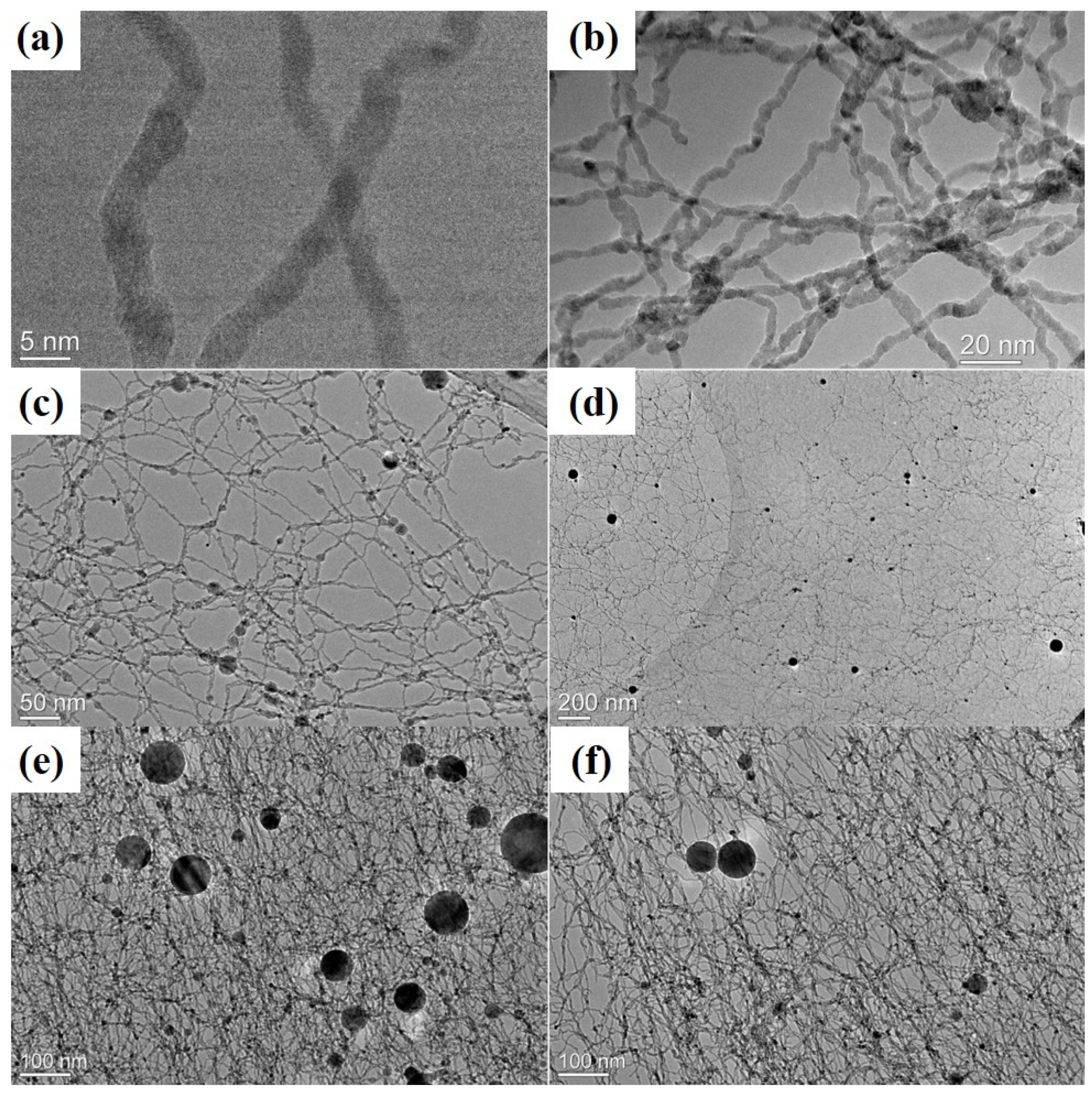
An SEM image of the large ball selected for the demonstration of fine details of its surface relief at a later stage of ablation (1 h) is shown in
Figure 2b. The share of such large particles is very small, and their contribution to size histogram is negligible. Similar relief on the ball surface can be distinguished in nanoballs of smaller diameters.
Figure 2b allows one to conclude that nanoballs and nanowires are not independently grown particles. The wrapping of the round Ni nuclei in curling nanowires is a possible mechanism of the growth of the balls.
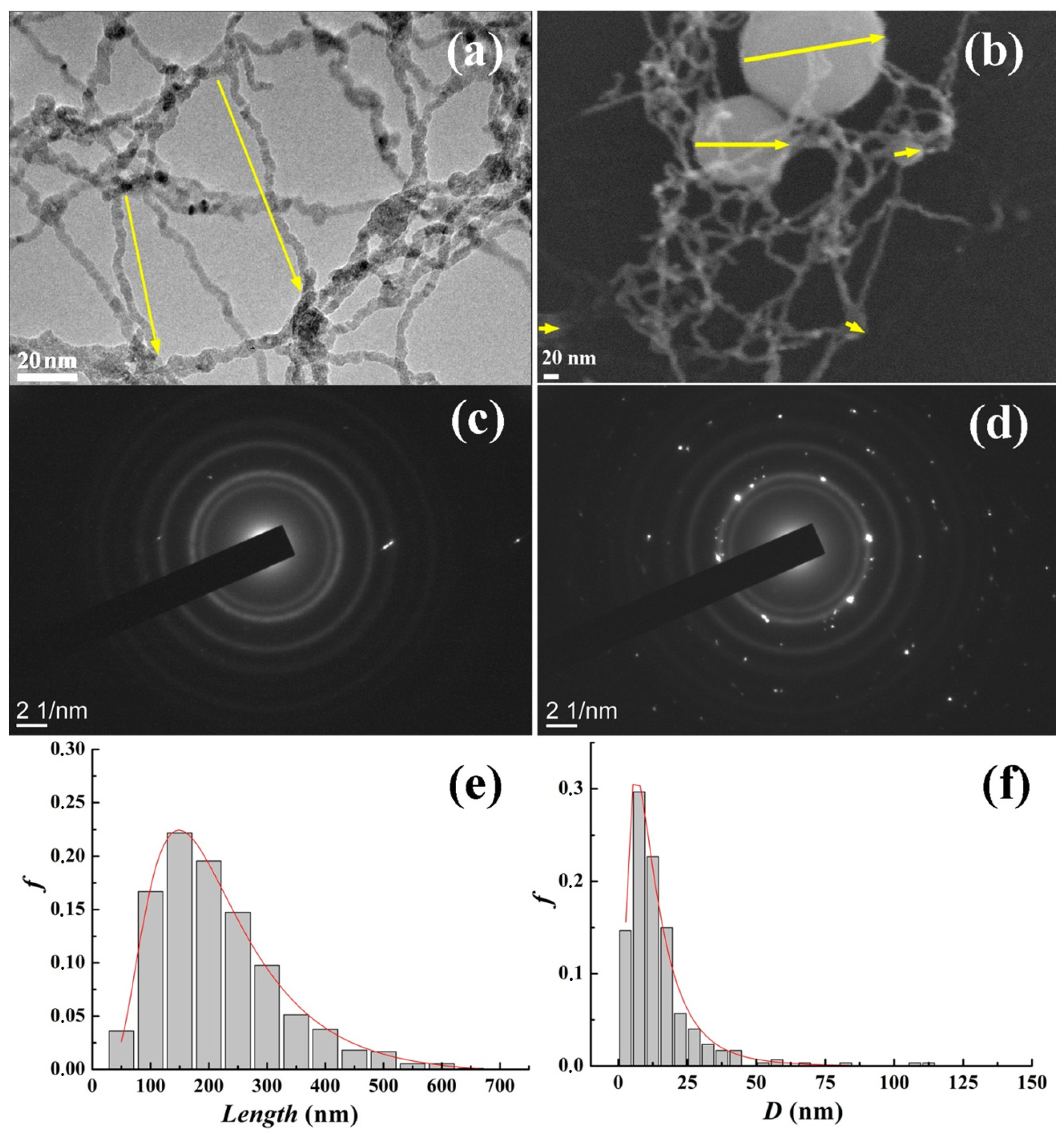
A TEM image of the Ni networks without balls at the early stage of 10 min ablation (
Figure 3a) and an SEM image of continuous nanowires network containing balls at the later stage of 20–60 min ablation (
Figure 3b–d) allow one to judge on the evolution of the system as the laser irradiation time and corresponding amount of Ni increase.
Figure 3c,d corresponds to the selected areas electron diffraction (SAED) of the parts of the networks corresponding to nanowires and nanoballs. No point reflexes can be found in SAED patterns of the nanowire (
Figure 3c), while clear patterns appear when the SAED of the nanoballs is recorded (
Figure 3d). Thus, the polycrystalline structure of the nanoballs and the highly disordered amorphous or nanocrystalline structure of nanowires are identified. According to multiple TEM images of different parts of the net, 2260 free nanowire segments and 70 balls have been treated statistically. The corresponding distribution of lengths of free Ni nanowires segments (
Figure 3e) and the distribution of nanoballs diameters (
Figure 3f) have been plotted. Statistical analysis of the nanowires and the nanoballs shows that both distributions follow the lognormal function (solid lines in
Figure 3e,f). The distributions indicate a wide enough scattering of geometrical sizes correspondingly to the chaotic process of the Ni distribution between He vortexes. Crystalline structure in the balls (
Figure 3d) suggests that they cannot consist of amorphous nanowires (
Figure 3c). Therefore, there are the following two mechanisms for increasing the size of the balls: (1) the growth of polycrystalline balls nucleated during ablation due to the absorption of nickel; (2) the winding of amorphous nanowires onto the nanoballs generated by ablation. It is reasonable to suppose that amorphous nanowires are formed at a very high cooling rate in He vortexes, while polycrystalline nanoballs are grown at a lower cooling rate in the He bulk. The series of net images used for statistical calculations are presented in
Supplementary Materials, Figure S1.
Images of the network at subsequent stages of laser ablation are presented in
Figure 4. Increase in size and number of nanoballs with ablation time can be distinguished.
Figure 5 presents a series of the hysteresis loops corresponding to the samples obtained at different ablation stages. The amount of Ni grows with ablation time. Field dependences were recorded at 300 K in the in-plane orientation of the magnetic field relative to the flat silicon substrate. The magnetic signal in the out-of-plane orientation is negligibly small. At the “in plane” orientation, there are fragments of nanowires perpendicular and parallel to the field, while at the “out-of-plane” orientation all the nanowires are perpendicular to the magnetic field. Since, in the out-of-plane orientation, the magnetic moment of the sample is lower than in the “in-plane” orientation, one can conclude that the easy magnetization axis of the nanowires is directed along their axis. One can conclude that the magnetic anisotropy of the nanowires is controlled by the shape anisotropy [
23].
Separation of the nanowires’ and nanoballs’ contributions can be reached by analysis of blocking temperatures on the temperature dependences of the magnetic moment recorded for the sample extracted at the later stage of ablation (60 min). At this stage, nanoballs give a valuable contribution, and the volume ratio of nanoballs to nanowires is 85:15, respectively (
Figure 5). The sample was cooled from 350 down to 2 K in an applied magnetic field of 1 T (FC mode). After cooling, the temperature dependence of the sample magnetic moment was recorded during heating in a weak magnetic field of 300 Oe (full symbols in
Figure 6). If the sample is cooled in a zero magnetic field (ZFC mode), the M(T) curve lies below the FC curve (empty symbols in
Figure 6).
The magnetic moment μ of an individual nanoball was determined using Magnetic Force Microscopy [
24]. The measured magnetic force was proportional to the second derivative of the magnetic field near the nanoball surface. The microscope response was directly proportional to the phase shift of the vibrating ferromagnetic Co cantilever scanning in the tapping-lift mode. Distribution of the local stray field of a single nanoball was scanned at different lift
h (the distance between the surface and cantilever tip). Images of the nanoball in Atomic Force Microscopy (AFM) and Magnetic Force Microscopy (MFM) modes were recorded (
Supplementary Materials, Figure S2a,b, correspondently). In AFM mode, the cantilever height above the surface was scanned, while in MFM mode, the phase shift was recorded as a function of the coordinate (
Supplementary Materials, Figure S2c,d, correspondently). The stray field of a single Ni nanoball with saturation magnetization
Ms equals the stray field of a point dipole positioned in its center. The lift value
h and the proportionality coefficient
c−1(
h) were measured to calculate the phase shift Δ
φ of the vibrating cantilever [
24] as follows:
We used the calibration algorithm proposed in [
24] to measure the calibration coefficient
c(
h). At
h = 50 nm, constant value
c = 0.04 A·nm
2 was obtained from the dependences of phase shift Δ
φ on diameter
d of nanoballs (
Supplementary Materials, Figure S3). Thus, the corresponding magnetic moment of a single nanoball of a 75-nanometer diameter is μ = 4.5 × 10
−19 A·m
2, which coincides well with the theoretically estimated value μ =
Msπ
d3/6 = 4.2 × 10
−19 A·m
2 calculated for a single domain nanoball of a 75-nanometer diameter. In addition, we have measured the field dependence of the magnetic moment (
Supplementary Materials, Figure S4). Though the approximation of the
m(
H) dependence and saturation magnetization
Ms = 510 emu/cm
3 are more or less convenient, the moments of the nanowires or nanoballs cannot be determined separately from the integrated magnetic moment, including contributions of objects of both types.
3. Discussion
Nickel nanowires and nanoparticles are widely reported in the literature. In particular, it is known that amorphous nano- and microwires have a rectangular magnetic hysteresis loop when they have a single-domain magnetic structure [
25,
26]. This property is called magnetic bistability, meaning that magnetization abruptly changes its direction when the polarity of the applied external field changes [
26], while a perpendicular magnetic field results in a sloping hysteresis loop. In a nano-network, where there are segments equiprobably directed in respect to the magnetic field, a change in the sign of the magnetic field can lead to an abrupt switching of the magnetization of those segments, whose direction is parallel to the field.
On the other hand, the resulting network can be presented as a non-continuous thin film, in which the easy magnetization axis lies in the plane of the film, as it is often observed for transition metal films. It is obvious that the above cases (a system of independent chaotically distributed nanowires and a thin discontinuous film) are limiting cases for our system. The real properties of the network lie between these two extreme cases.
When the ablation time and Ni amount increase, the saturation magnetic moment
ms also increases, while the coercive field
HC decreases (
Figure 5). We decomposed the recorded hysteresis loops into two contributions from nanowires and from nanoballs in accordance with the following expression [
25]:
where indexes
i = 1 and
i = 2 correspond to nanowires and balls, respectively; signs «+» and «−» correspond to the descending and ascending parts of the hysteresis loops;
ms is the magnetic moment at saturation;
H is the external magnetic field; and
are the respective coercive fields of nanowires and nanoballs. The adjustment of coefficients
pi to reach a true hysteresis loop shape (
Figure 5) allowed us to determine the parameters characterizing the rectangularity of the hysteresis loops,
p1 = 0.95 for nanowires and
p2 = 0.45 for nanoballs. One can see the following two components: a rectangular component belonging to the nanowires and a sloped component corresponding to the nanoballs. We took into account the demagnetizing factors (2/3 for ball and 2π for cylinder) and calculated the relative volume shares of the Ni nanowires and nanoballs at different stages of ablation. In the insets to each hysteresis loop (
Figure 5), one can find a circle diagram indicating the relative volume fractions of the nanowires and nanoballs. Simple regularity follows from the comparison of the hysteresis shapes and volume fraction of the nanoballs. The rectangularity of the hysteresis loop decreases as the number of nanoballs grows.
Figure 7 shows the increasing dependence of the saturation magnetic moment
mS of the sample for the entire amount of nickel on the ablation time (curve one). Since the saturation magnetization of nickel
Ms = 58.6 emu/g (522 emu/cm
3) is well known [
27], and there is no reason to think that the magnetic moment in saturation can change due to variations in
ms, the increase in the Ni amount on the substrate is the only reason for the increasing
m. It is impossible to determine the mass of nickel deposited on the substrate in another way since it is very small as compared to the mass of the substrate. We can estimate the order of value of Ni yield using an increase in the absolute value of the magnetic moment of the Si substrate Δ
m ~ 10
−6–10
−5 emu caused by network formation. Using the known in advance saturation magnetization
Ms = 58.6 emu/g of Ni, we can determine the network mass Δ
m/Ms ~ 10
−8–10
−7 g.
Since we know the percentage ratio for the volume of nanowires and the volume of nanospheres at each stage of the formation of a nanowire (
Figure 5), we have plotted the dependences of the magnetic moment of nanoballs and nanowires on ablation time separately (
Figure 7, curves two and three, respectively). It is seen that at the later stage of ablation, the main additional contribution to the magnetic moment
m is provided by nanoballs, the number and size of which increase with the ablation time. The straightening of curves 1–3 in ln(
m)–ln(
t) coordinates (
Figure 7) corresponds to the power law of the
m(
t) dependence
m ~
tn,
n = 1.36 > 1. If one assumes that the nickel mass increases linearly with the ablation time, the power law corresponds to a situation when the magnetic properties of the system depend on its size. In our experiments, the gradually changing ratio of the number of nanowires to that of nanoballs as well as the formation of a network are possible reasons for a superlinear
m(
t) dependence.
The magnetic anisotropy of the bulk Ni crystal is
Kbulk = −5.12 × 10
4 erg/cm
3 [
23,
28], and its value diminishes due to spin disorder in the surface layer of a 1–2-nanometer depth. Since shape anisotropy is one order of magnitude higher than crystalline anisotropy constant
Ksh = 7.4 × 10
4 J m
−3 = 7.4 × 10
5 erg/cm
−3 and has the opposite sign, an effective anisotropy field is only due to the shape anisotropy in the nickel nanowire. Neglecting crystalline anisotropy, one can obtain an effective anisotropy field of a single segment of nanowire as
Heff = 2
πMs = 243 kA m
−1 = 3042 Oe. This value is quite high in comparison with
Hc = 500 Oe obtained in pure nanowires at the early ablation stage (
Figure 5a). A similar value of coercive field
HC can be obtained from the Neel–Brawn formula allowing one to calculate the coercive field of a single domain particle
HC = 2
Ksh/
Ms = 2874 Oe.
The typical domain wall width in Ni is
lw = 2(
A/
Ksh)
1/2 = 30 nm, where
A is the exchange stiffness of Ni and thereby the multidomain structure within a single wire is likely to form if the nanowire diameter exceeds 30 nm. In fact, single domain nanowires are usually obtained in wire with a diameter narrowing or of the same order as
lw~30 nm and showing coercivity of about 1000 Oe [
25,
26]. We have obtained coercivity 500 Oe for samples at the early ablation stage, where nanowires 1–2 nm in diameter are presented in the absence of nanoballs. Thus, one should conclude that domain motion should be excluded to explain the decreased
Hc value of 500 Oe in the frames of the independent nanowires model. The diminished value of an experimentally determined switching field in the system under study may differ from that predicted theoretically for independent nanowires because non-coherent switching modes, such as curling and fanning, can contribute to magnetization reversal. We should take into account that the wires are connected to each other in our samples. This affects both the demagnetization field and shape factor, and the estimation of the single domain limit. The presence of junctions of nanowires can facilitate propagation of the domain walls or nucleation of the magnetic reversal phase at 500 Oe, i.e., properties of the magnetic network are different from properties of single nanowires.
A simple expression connecting magnetic anisotropy and blocking temperature is valid for nanoballs. We used the formula applicable for the determination of blocking temperature
TB in a SQUID magnetometer [
29], which is as follows:
This formula allows one to estimate the blocking temperatures
TB by substituting effective anisotropy constant
Keff and particle volume
V into Equation (3). If we substitute the shape anisotropy of nanoballs that decreased due to form factor
KA = 2/3π
Ms = 0.74 · 10
5 erg/cm
3 instead of
Keff, and
Vball ≈ 4.2 · 10
−18 nm
3 corresponding to the average diameter of the balls of 5 nm at the later stage of ablation (see histogram in
Figure 3f) into Equation (3), we can obtain
TB = 548 K. This value coincides well with that found by the extrapolation of the FC and ZFC dependences to their intersection (
Figure 6). According to the Neel–Brown theory, in the system of non-interacting separated nanoparticles, the temperature corresponding to the maximum of the
M(
T) curve is exactly equal to the blocking temperature
Tb [
30]. The crossing point of the FC and ZFC curves is very close to the blocking temperature, and we assume an approximate equality of these temperatures
Tc ≈
Tb neglecting the interparticle interaction.
Thus, 548 K is an average blocking temperature for the nanoballs, while maximum on the ZFC curve near 235 K is obviously blocking temperature for the nanowire network. The blocking temperatures of nanoballs and nanowires are both below the Curie temperature of 631 K for the bulk Ni sample.
4. Materials and Methods
Low-temperature synthesis of the nanowires was carried out in an optical helium cryostat (
Supplementary Materials, Figure S5a). Bottom part of the cryostat was equipped with quartz windows. Ni target was placed inside the cryostat in front of the window. The cryostat was filled with liquid helium at 4.2 K, and the temperature decrease down to 1.5 K was attained by pumping. Then, helium was transferred to the superfluid phase. Laser ablation of the Ni target was carried out using an LSB diode-pumped Nd laser with pulse duration of 0.4 ns, pulse repetition of 4 kHz, pulse energy of 0.1 mJ and wavelength of 1.062 μm (
Supplementary Materials, Figure S5b). Laser irradiation was focused on the target Ni surface. Duration of laser ablation was varied depending on desirable Ni concentration in helium. We placed a permanent magnet inside the cryostat to attract ferromagnetic products to the Si substrate to obtain larger amount of the products.
In general, the process of growth was the following. Laser-induced evaporation of the Ni target was accompanied by generation of quantum vortices (
Figure 1b). At the first stage of ablation, series of isolated individual nanowires were observed at a low concentration of Ni. At the second stage when concentration of the nanowires increased, one observed the formation of a net (
Figure 1c). At the third stage at high concentrations of Ni, nanowires reeled to the balls. Ablation products formed a net deposited on silicon substrate of 1 × 1 × 4 mm
3 size, which was covered by TEM grid and placed at the bottom of the cryostat (
Figure 1d).
Microstructure, morphology and local elemental analyses were carried out using a JEM-2100 transmission electron microscope (TEM) (JEOL, Benelux, Welwyn Garden, England) and a Zeiss Supra 25 scanning electron microscope (SEM) (Carl Zeiss AG, Oberkochen, Germany) with energy dispersive microanalysis (EDX). EDX analysis indicated 99% Ni and 1% O contained in a single Ni ball (
Figure 2a). TEM picture of a separate nanoball clearly indicated multiple nanowires reeled on a ball (
Figure 2b).
Magnetic properties of the net deposited on Si wafer were recorded using a MPMX 5XL (Quantum Design SQUID magnetometer, Berlin, Germany) at different stages of the structure formation. Magnetic moment of the individual nanoball was recorded using an Integra-Aura (NT MDT, Moscow, Russia) atomic and magnetic force microscope. Two-pass tapping-lift algorithm of MFM scanning provided high accuracy of measurements. We used a standard silicon based MFM LM cantilever covered by thin CoCr film.


