
Recent Advancements in Applications of Graphene to Attain Next-Level Solar Cells

Abstract
:1. Introduction
2. Methodology: Graphene Synthesis Techniques and Graphene Transfer
2.1. Mechanical Exfoliation
2.2. Chemical Exfoliation
2.3. Chemical Synthesis and Functionalizations
2.4. Thermal CVD Process
2.5. Epitaxial Growth
2.6. Graphene Transfer
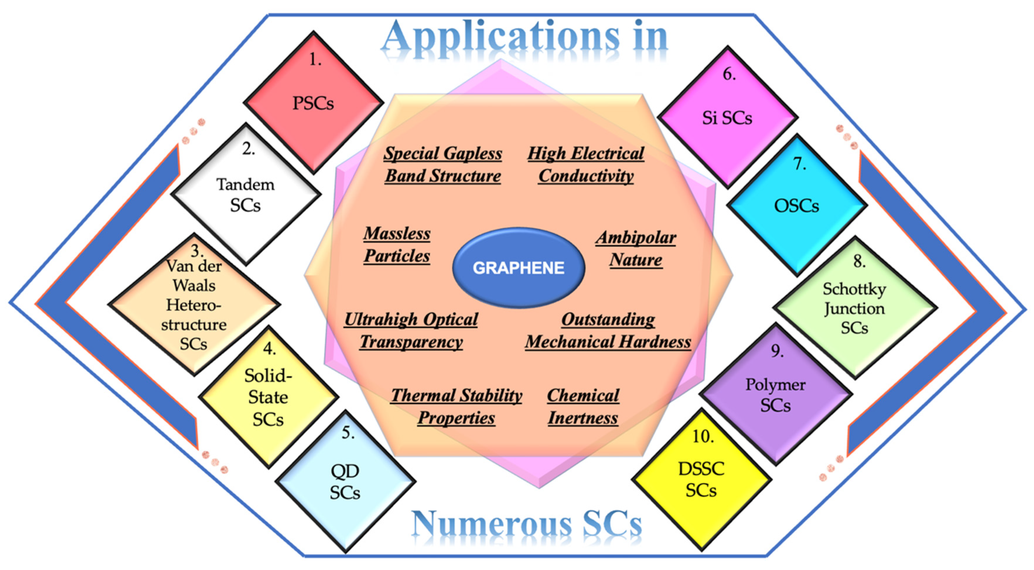
3. Impact of Graphene on SC Technology
3.1. Controllable Graphene Parameters for High Efficiency of SCs
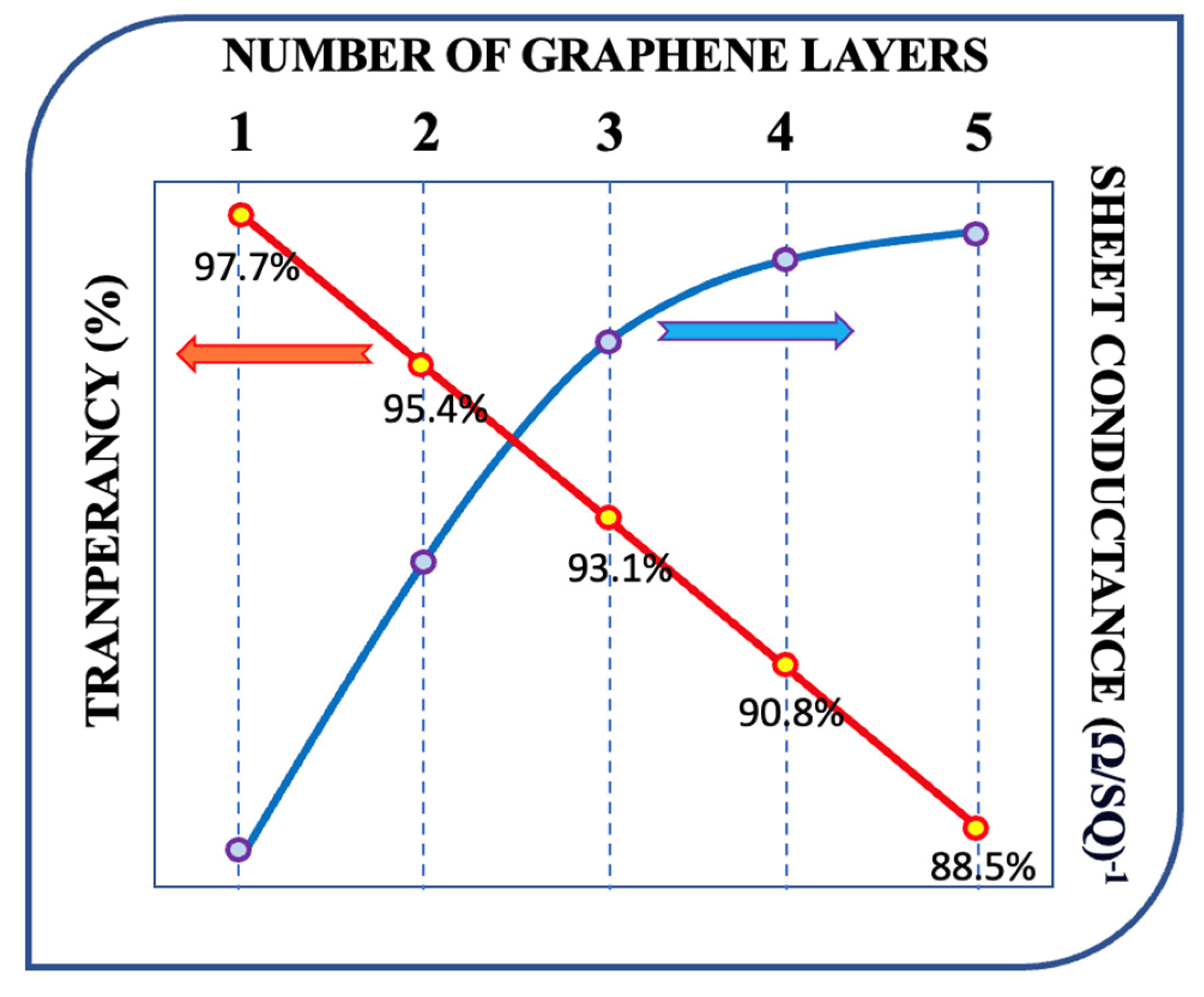
3.1.1. Impact of Graphene Layer Thickness on SC Efficiency
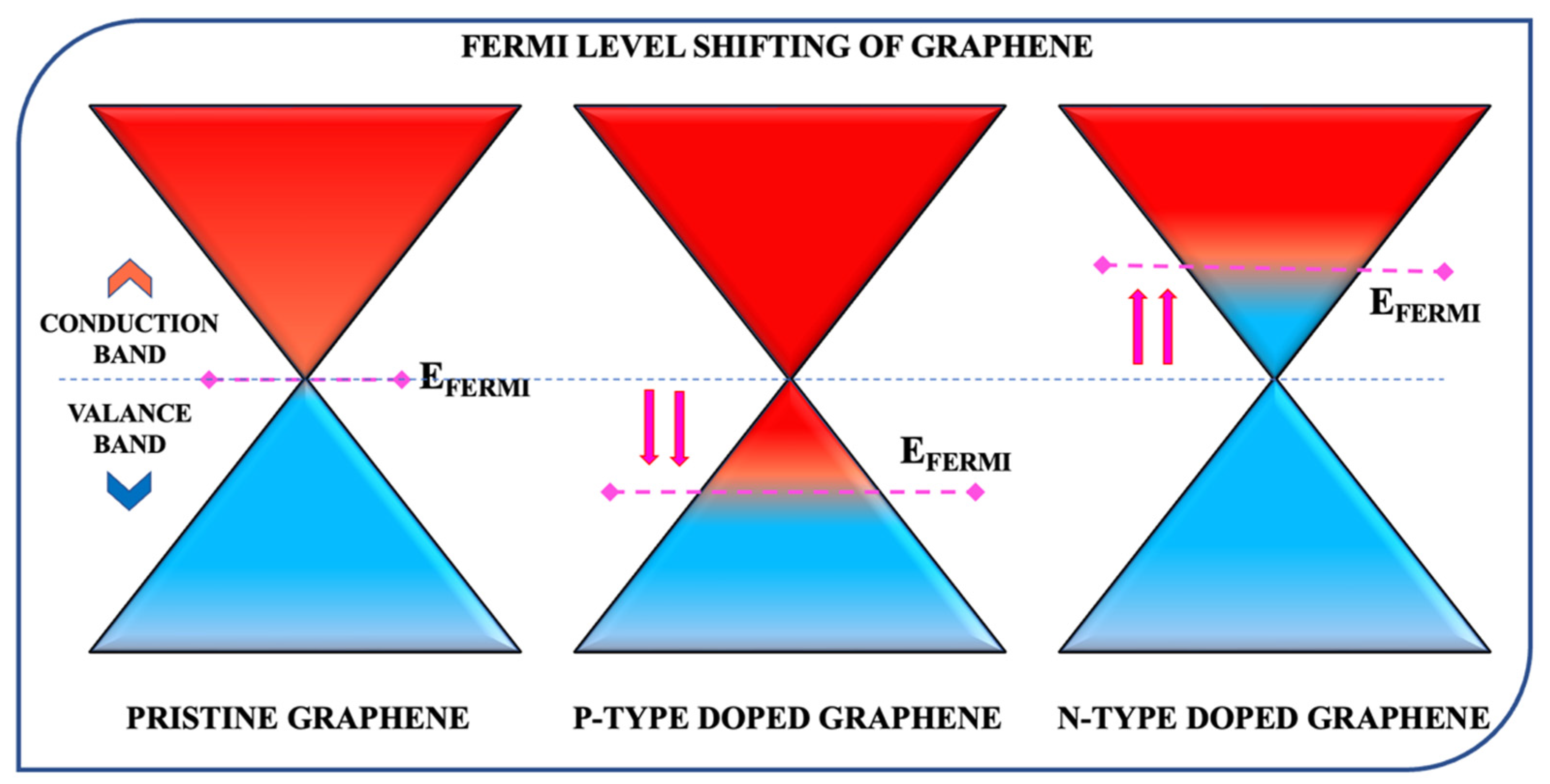
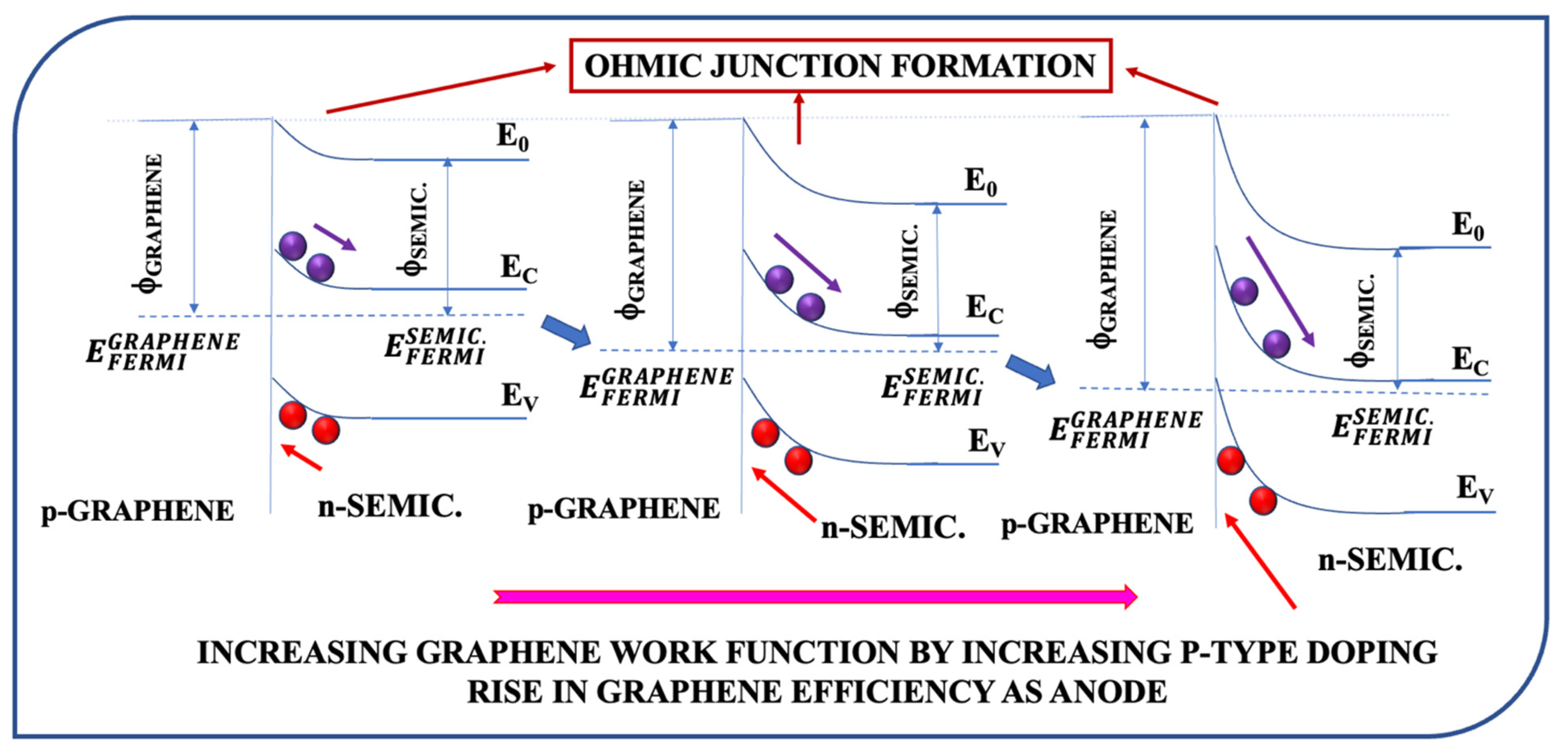
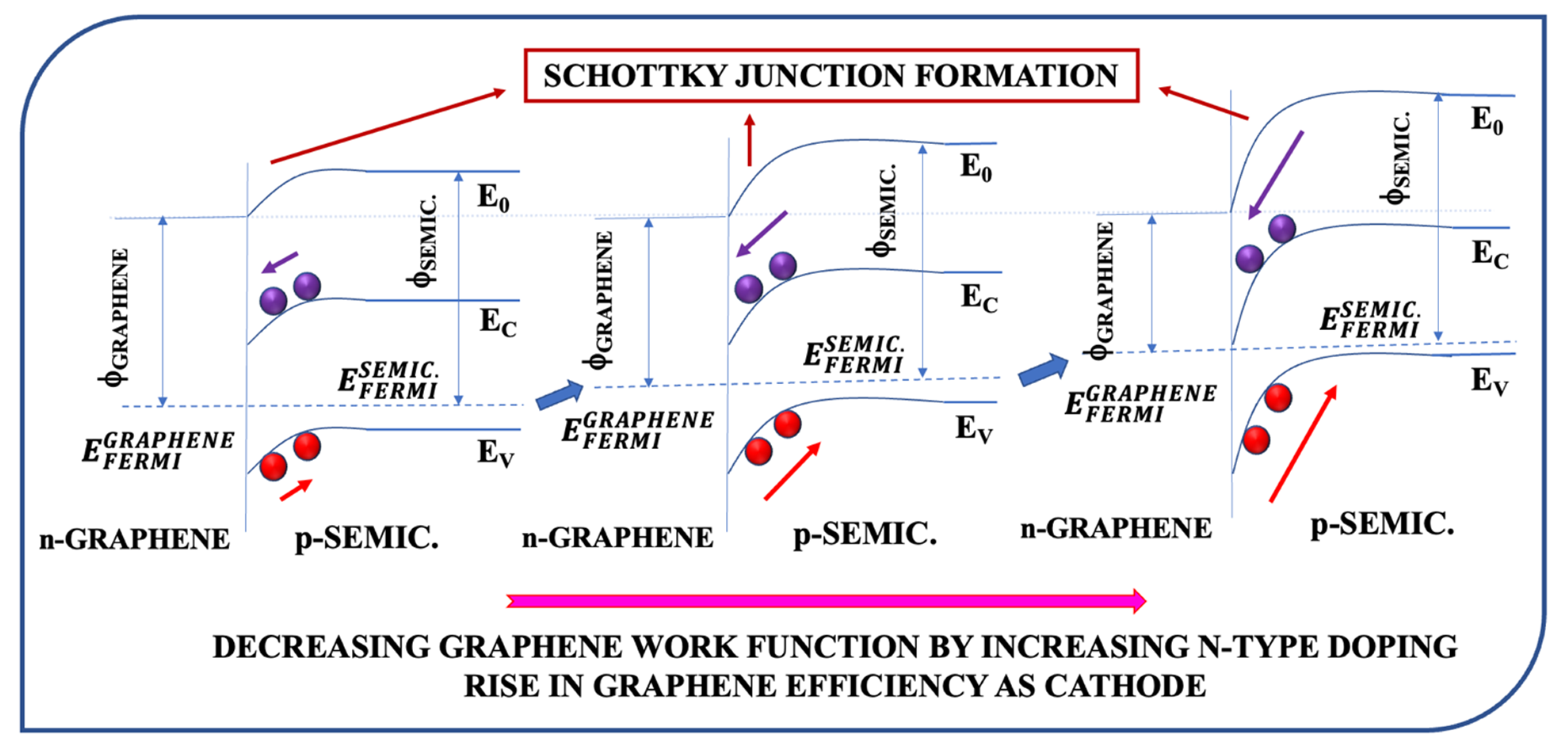
3.1.2. Impact of Graphene Doping on SC Efficiency
3.2. Different Roles of Graphene in PV Technology
3.2.1. Graphene Transparent Conducting Electrodes
3.2.2. Graphene Photoactive Layers
3.2.3. Graphene Schottky Junctions
3.3. Application of Graphene in Various Types of SCs
3.3.1. Application of Graphene in Silicon SCs: The Graphene/Si SCs
Application of Graphene in Porous Silicon SC: Graphene/PSi SC
Application of Graphene in Silicon Nanowires SCs: Graphene/Si NWs SC
Application of Graphene in Silicon Quantum Dot SCs: Graphene/Si QD SC
3.3.2. Application of Graphene in Polymer SC: Graphene/Polymer SC
3.3.3. Application of Graphene in Schottky Junction Solar Cells: Graphene/Schottky Junction SC
3.3.4. Application of Graphene in Dye-Sensitized SC: Graphene-Based DSSCs
Application of Graphene as Photoanode in DSSCs
Application of Graphene as Counter Electrode Material in DSSCs
Application of Graphene as Sensitizing Material in DSSCs
Application of Graphene as Photoanode Additive in DSSCs
3.3.5. Application of Graphene in Quantum Dot SCs: Graphene-Based QD SC
3.3.6. Application of Graphene in Graphene/Semiconductor Van der Waals Heterostructure SCs
3.3.7. Application of Graphene in Tandem SCs: Graphene-Based Tandem SC
3.3.8. Application of Graphene in Perovskite SCs: Graphene-Based PSC
Application of Graphene as Charge Transport Layer in PSCs
Application of Graphene as Electrodes in PSCs
Application of Graphene as Stabilizing Material in PSCs
3.3.9. Application of Graphene in Organic SCs: Graphene-Based OSC
Application of Graphene as Electrodes in Graphene-Based OSCs
Application of Graphene as Charge Transport Layer in Graphene-Based OSCs
Application of Graphene as Ternary Material in Graphene-Based OSCs
3.3.10. Application of Graphene in Solid-State SCs: Graphene-Based Solid-State SC
4. Conclusions and Perspective
Author Contributions
Funding
Data Availability Statement
Conflicts of Interest
References
- Nadarajah, K.; Vakeesan, D. Solar energy for future world: A review. Renew. Sustain. Energy Rev. 2016, 62, 1092–1105. [Google Scholar]
- Das, S.; Sudhagar, P.; Kang, Y.S.; Choi, W. Graphene synthesis and application for solar cells. J. Mater. Res. 2014, 29, 299–319. [Google Scholar] [CrossRef] [Green Version]
- Novoselov, K.S.; Geim, A.K.; Morozov, S.V.; Jiang, D.E.; Zhang, Y.; Dubonos, S.V.; Grigorieva, I.V.; Firsov, A.A. Electric field effect in atomically thin carbon films. Science 2004, 306, 666–669. [Google Scholar] [CrossRef] [PubMed] [Green Version]
- Burghard, M.; Hagen, K.; Klaus, K. Carbon-based field-effect transistors for nanoelectronics. Adv. Mater. 2009, 21, 2586–2600. [Google Scholar] [CrossRef]
- Behura, S.K.; Mahala, P.; Nayak, S.; Yang, Q.; Mukhopadhyay, I.; Jani, O. Fabrication of bi-layer graphene and theoretical simulation for its possible application in thin film solar cell. J. Nanosci. Nanotechnol. 2014, 14, 3022–3027. [Google Scholar] [CrossRef] [PubMed]
- Tamandani, S.; Darvish, G.; Faez, R. Analytical calculation of energy levels of mono-and bilayer graphene quantum dots used as light absorber in solar cells. Appl. Phys. A 2016, 122, 37. [Google Scholar] [CrossRef]
- Radamson, H.H. Graphene. In Springer Handbook of Electronic and Photonic Materials; Springer: Berlin/Heidelberg, Germany, 2017; p. 1. [Google Scholar]
- Bahri, M.; Gebre, S.H.; Elaguech, M.A.; Dajan, F.T.; Sendeku, M.G.; Tlili, C.; Wang, D. Recent advances in chemical vapour deposition techniques for graphene-based nanoarchitectures: From synthesis to contemporary applications. Coord. Chem. Rev. 2023, 475, 214910. [Google Scholar] [CrossRef]
- Das, S.; Pandey, D.; Thomas, J.; Roy, T. The role of graphene and other 2D materials in solar photovoltaics. Adv. Mater. 2019, 31, 1802722. [Google Scholar] [CrossRef] [Green Version]
- Nandi, A.; Majumdar, S.; Datta, S.K.; Saha, H.; Hossain, S.M. Optical and electrical effects of thin reduced graphene oxide layers on textured wafer-based c-Si solar cells for enhanced performance. J. Mater. Chem. C 2017, 5, 1920–1934. [Google Scholar] [CrossRef]
- Wendler, F.; Knorr, A.; Malic, E. Carrier multiplication in graphene under Landau quantization. Nat. Commun. 2014, 5, 3703. [Google Scholar] [CrossRef] [Green Version]
- Balandin, A.A. Thermal properties of graphene and nanostructured carbon materials. Nat. Mater. 2011, 10, 569–581. [Google Scholar] [CrossRef] [PubMed] [Green Version]
- Akinwande, D.; Brennan, C.J.; Bunch, J.S.; Egberts, P.; Felts, J.R.; Gao, H.; Huang, R.; Kim, J.S.; Li, T.; Li, Y.; et al. A review on mechanics and mechanical properties of 2D materials—Graphene and beyond. Extrem. Mech. Lett. 2017, 13, 42–77. [Google Scholar] [CrossRef] [Green Version]
- Papageorgiou, D.G.; Ian, A.K.; Robert, J.Y. Mechanical properties of graphene and graphene-based nanocomposites. Prog. Mater. Sci. 2017, 90, 75–127. [Google Scholar] [CrossRef]
- Behura, S.K.; Mahala, P.; Ray, A.; Mukhopadhyay, I.; Jani, O. Theoretical simulation of photovoltaic response of graphene-on-semiconductors. Appl. Phys. A 2013, 111, 1159–1163. [Google Scholar] [CrossRef]
- Craighead, H.G.; Julian, C.; Hackwood, S. New display based on electrically induced index-matching in an inhomogeneous medium. Appl. Phys. Lett. 1982, 40, 22–24. [Google Scholar] [CrossRef]
- Xia, S.; Huang, W.; Yan, W.; Yuan, X.; Chen, X.; Liu, L.; Fu, L.; Zhu, Y.; Huang, Q.; Wu, Y.; et al. A Separator Modified with Rutile Titania and Three-Dimensional Interconnected Graphene-Like Carbon for Advanced Li−S Batteries. ChemElectroChem 2022, 9, e202200301. [Google Scholar] [CrossRef]
- Wang, G.; Shen, X.; Yao, J.; Park, J. Graphene nanosheets for enhanced lithium storage in lithium ion batteries. Carbon 2009, 47, 2049–2053. [Google Scholar] [CrossRef]
- Cai, X.; Lai, L.; Shen, Z.; Lin, J. Graphene and graphene-based composites as Li-ion battery electrode materials and their application in full cells. J. Mater. Chem. A 2017, 5, 15423–15446. [Google Scholar] [CrossRef]
- Cheng, Q.; Okamoto, Y.; Tamura, N.; Tsuji, M.; Maruyama, S.; Matsuo, Y. Graphene-like-graphite as fast-chargeable and high-capacity anode materials for lithium ion batteries. Sci. Rep. 2017, 7, 14782. [Google Scholar] [CrossRef] [Green Version]
- Wang, F.; Wang, C.; Zhao, Y.; Liu, Z.; Chang, Z.; Fu, L.; Zhu, Y.; Wu, Y.; Zhao, D. A quasi-solid-state Li-ion capacitor based on porous TiO2 hollow microspheres wrapped with graphene nanosheets. Small 2016, 12, 6207–6213. [Google Scholar] [CrossRef]
- Wang, F.; Liu, Z.; Yuan, X.; Mo, J.; Li, C.; Fu, L.; Zhu, Y.; Wu, X.; Wu, Y. A quasi-solid-state Li-ion capacitor with high energy density based on Li 3 VO 4/carbon nanofibers and electrochemically-exfoliated graphene sheets. J. Mater. Chem. A 2017, 5, 14922–14929. [Google Scholar] [CrossRef]
- Ke, Q.; Wang, J. Graphene-based materials for supercapacitor electrodes—A review. J. Mater. 2016, 2, 37–54. [Google Scholar] [CrossRef] [Green Version]
- Tan, Y.B.; Jong-Min, L. Graphene for supercapacitor applications. J. Mater. Chem. A 2013, 1, 14814–14843. [Google Scholar] [CrossRef]
- Yang, W.; Ni, M.; Ren, X.; Tian, Y.; Li, N.; Su, Y.; Zhang, X. Graphene in supercapacitor applications. Curr. Opin. Colloid Interface Sci. 2015, 20, 416–428. [Google Scholar] [CrossRef]
- Yang, H.; Kannappan, S.; Pandian, A.S.; Jang, J.H.; Lee, Y.S.; Lu, W. Graphene supercapacitor with both high power and energy density. Nanotechnology 2017, 28, 445401. [Google Scholar] [CrossRef] [Green Version]
- Vivekchand, S.R.C.; Rout, C.S.; Subrahmanyam, K.S.; Govindaraj, A.; Rao, C.N.R. Graphene-based electrochemical supercapacitors. J. Chem. Sci. 2008, 120, 9–13. [Google Scholar] [CrossRef]
- Ou, Z.; An, Z.; Ma, Z.; Li, N.; Han, Y.; Yang, G.; Jiang, Q.; Chen, Q.; Chu, W.; Wang, S.; et al. 3D Porous Graphene-like Carbons Encaged Single-Atom-Based Pt for Ultralow Loading and High-Performance Fuel Cells. ACS Catal. 2023, 13, 1856–1862. [Google Scholar] [CrossRef]
- Choi, H.J.; Jung, S.M.; Seo, J.M.; Chang, D.W.; Dai, L.; Baek, J.B. Graphene for energy conversion and storage in fuel cells and supercapacitors. Nano Energy 2012, 1, 534–551. [Google Scholar] [CrossRef]
- Shaari, N.; Kamarudin, S.K. Graphene in electrocatalyst and proton conductiong membrane in fuel cell applications: An overview. Renew. Sustain. Energy Rev. 2017, 69, 862–870. [Google Scholar] [CrossRef]
- Farooqui, U.R.; Abdul, L.A.; Hamid, N.A. Graphene oxide: A promising membrane material for fuel cells. Renew. Sustain. Energy Rev. 2018, 82, 714–733. [Google Scholar] [CrossRef]
- Li, J.; Chen, J.; Shen, B.; Yan, X.; Xue, Q. Temperature dependence of the field emission from the few-layer graphene film. Appl. Phys. Lett. 2011, 99, 163103. [Google Scholar] [CrossRef]
- Ye, D.; Moussa, S.; Ferguson, J.D.; Baski, A.A.; El-Shall, M.S. Highly efficient electron field emission from graphene oxide sheets supported by nickel nanotip arrays. Nano Lett. 2012, 12, 1265–1268. [Google Scholar] [CrossRef] [PubMed]
- Dikin, D.A.; Stankovich, S.; Zimney, E.J.; Piner, R.D.; Dommett, G.H.; Evmenenko, G.; Nguyen, S.T.; Ruoff, R.S. Preparation and characterization of graphene oxide paper. Nature 2007, 448, 457–460. [Google Scholar] [CrossRef] [PubMed]
- Li, G.L.; Liu, G.; Li, M.; Wan, D.; Neoh, K.G.; Kang, E.T. Organo-and water-dispersible graphene oxide−polymer nanosheets for organic electronic memory and gold nanocomposites. J. Phys. Chem. C 2010, 114, 12742–12748. [Google Scholar] [CrossRef]
- Zande, A.M.V.D.; Barton, R.A.; Alden, J.S.; Ruiz-Vargas, C.S.; Whitney, W.S.; Pham, P.H.; Park, J.; Parpia, J.M.; Craighead, H.G.; McEuen, P.L. Large-scale arrays of single-layer graphene resonators. Nano Lett. 2010, 10, 4869–4873. [Google Scholar] [CrossRef]
- Schedin, F.; Geim, A.K.; Morozov, S.V.; Hill, E.W.; Blake, P.; Katsnelson, M.I.; Novoselov, K.S. Detection of individual gas molecules adsorbed on graphene. Nat. Mater. 2007, 6, 652–655. [Google Scholar] [CrossRef] [PubMed]
- Xia, F.; Mueller, T.; Lin, Y.M.; Valdes-Garcia, A.; Avouris, P. Ultrafast graphene photodetector. Nat. Nanotechnol. 2009, 4, 839–843. [Google Scholar] [CrossRef] [Green Version]
- Wang, J.X.; Lai, H.; Zhong, M.; Liu, X.; Chen, Y.; Yao, S. Design and Scalable Fabrication of Liquid Metal and Nano-Sheet Graphene Hybrid Phase Change Materials for Thermal Management. Small Methods 2023, 2300139. [Google Scholar] [CrossRef]
- Palacios, T. Thinking outside the silicon box. Nat. Nanotechnol. 2011, 6, 464–465. [Google Scholar] [CrossRef]
- Han, W.; Kawakami, R.K.; Gmitra, M.; Fabian, J. Graphene spintronics. Nat. Nanotechnol. 2014, 9, 794–807. [Google Scholar] [CrossRef] [Green Version]
- Yu, X.; Cheng, H.; Zhang, M.; Zhao, Y.; Qu, L.; Shi, G. Graphene-based smart materials. Nat. Rev. Mater. 2017, 2, 17046. [Google Scholar] [CrossRef]
- Song, Y.; Luo, Y.; Zhu, C.; Li, H.; Du, D.; Lin, Y. Recent advances in electrochemical biosensors based on graphene two-dimensional nanomaterials. Biosens. Bioelectron. 2016, 76, 195–212. [Google Scholar] [CrossRef] [PubMed]
- Kumar, S.; Duesberg, G.S.; Pratap, R.; Raghavan, S. Graphene field emission devices. Appl. Phys. Lett. 2014, 105, 103107. [Google Scholar] [CrossRef] [Green Version]
- Ahn, J.-H.; Byung, H.H. Graphene for displays that bend. Nat. Nanotechnol. 2014, 9, 737–738. [Google Scholar] [CrossRef] [PubMed]
- Polat, E.O.; Balci, O.; Kakenov, N.; Uzlu, H.B.; Kocabas, C.; Dahiya, R. Synthesis of large area graphene for high performance in flexible optoelectronic devices. Sci. Rep. 2015, 5, 16744. [Google Scholar] [CrossRef] [PubMed] [Green Version]
- Kostarelos, K.; Vincent, M.; Hebert, C.; Garrido, J.A. Graphene in the design and engineering of next-generation neural interfaces. Adv. Mater. 2017, 29, 1700909. [Google Scholar] [CrossRef]
- Nguyen, B.H.; Nguyen, V.H. Promising applications of graphene and graphene-based nanostructures. Adv. Nat. Sci. Nanosci. Nanotechnol. 2016, 7, 023002. [Google Scholar] [CrossRef] [Green Version]
- Liao, L.; Xiangfeng, D. Graphene for radio frequency electronics. Mater. Today 2012, 15, 328–338. [Google Scholar] [CrossRef]
- Zhu, W.; Perebeinos, V.; Freitag, M.; Avouris, P. Carrier scattering, mobilities, and electrostatic potential in monolayer, bilayer, and trilayer graphene. Phys. Rev. B 2009, 80, 235402. [Google Scholar] [CrossRef] [Green Version]
- Nandi, A.; Dhar, S.; Majumdar, S.; Saha, H.; Hossain, S.M. Performance Enhancement of Solar Cell by Incorporating Bilayer RGO-ITO Smart Conducting Antireflection Coating. Glob. Chall. 2019, 3, 1800109. [Google Scholar] [CrossRef]
- Becerril, H.A.; Mao, J.; Liu, Z.; Stoltenberg, R.M.; Bao, Z.; Chen, Y. Evaluation of solution-processed reduced graphene oxide films as transparent conductors. ACS Nano 2008, 2, 463–470. [Google Scholar] [CrossRef] [PubMed]
- Kim, K.S.; Zhao, Y.; Jang, H.; Lee, S.Y.; Kim, J.M.; Kim, K.S.; Ahn, J.H.; Kim, P.; Choi, J.Y.; Hong, B.H. Large-scale pattern growth of graphene films for stretchable transparent electrodes. Nature 2009, 457, 706–710. [Google Scholar] [CrossRef]
- Huang, H.; Chen, W.; Chen, S.; Wee, A.T.S. Bottom-up growth of epitaxial graphene on 6H-SiC (0001). ACS Nano 2008, 2, 2513–2518. [Google Scholar] [CrossRef] [PubMed]
- Tung, V.C.; Allen, M.J.; Yang, Y.; Kaner, R.B. High-throughput solution processing of large-scale graphene. Nat. Nanotechnol. 2009, 4, 25–29. [Google Scholar] [CrossRef] [PubMed]
- Reina, A.; Jia, X.; Ho, J.; Nezich, D.; Son, H.; Bulovic, V.; Dresselhaus, M.S.; Kong, J. Large area, few-layer graphene films on arbitrary substrates by chemical vapor deposition. Nano Lett. 2009, 9, 30–35. [Google Scholar] [CrossRef] [PubMed]
- Shi, P.C.; Guo, J.P.; Liang, X.; Cheng, S.; Zheng, H.; Wang, Y.; Chen, C.H.; Xiang, H.F. Large-scale production of high-quality graphene sheets by a non-electrified electrochemical exfoliation method. Carbon 2018, 126, 507–513. [Google Scholar] [CrossRef] [Green Version]
- Li, J.; Yan, H.; Dang, D.; Wei, W.; Meng, L. Salt and water co-assisted exfoliation of graphite in organic solvent for efficient and large scale production of high-quality graphene. J. Colloid Interface Sci. 2019, 535, 92–99. [Google Scholar] [CrossRef]
- Islam, A.; Mukherjee, B.; Pandey, K.K.; Keshri, A.K. Ultra-fast, chemical-free, mass production of high quality exfoliated graphene. ACS Nano 2021, 15, 1775–1784. [Google Scholar] [CrossRef]
- Shi, Z.; He, P.; Wang, N.; Liu, Y.; Chen, X.; Li, Y.; Ding, G.; Yu, Q.; Xie, X. Bubble-Mediated Mass Production of Graphene: A Review. Adv. Funct. Mater. 2022, 32, 2203124. [Google Scholar] [CrossRef]
- Qiao, C.; Che, J.; Wang, J.; Wang, X.; Qiu, S.; Wu, W.; Chen, Y.; Zu, X.; Tang, Y. Cost effective production of high quality multilayer graphene in molten Sn bubble column by using CH4 as carbon source. J. Alloys Compd. 2023, 930, 167495. [Google Scholar] [CrossRef]
- Geim, A.K.; Novoselov, K.S. The rise of graphene. Nat. Mater. 2007, 6, 183–191. [Google Scholar] [CrossRef] [PubMed]
- Viculis, L.M.; Mack, J.J.; Kaner, R.B. A Chemical Route to Carbon Nanoscrolls. Science 2003, 299, 1361. [Google Scholar] [CrossRef] [PubMed]
- Hernandez, Y.; Nicolosi, V.; Lotya, M.; Blighe, F.M.; Sun, Z.; De, S.; McGovern, I.T.; Holland, B.; Byrne, M.; Gun’Ko, Y.K.; et al. High-yield production of graphene by liquid-phase exfoliation of graphite. Nat. Nanotechnol. 2008, 3, 563–568. [Google Scholar] [CrossRef] [Green Version]
- Wintterlin, J.; Bocquet, M.-L. Graphene on metal surfaces. Surf. Sci. 2009, 603, 1841–1852. [Google Scholar] [CrossRef]
- Berger, C.; Song, Z.; Li, T.; Li, X.; Ogbazghi, A.Y.; Feng, R.; Dai, Z.; Marchenkov, A.N.; Conrad, E.H.; First, P.N.; et al. Ultrathin epitaxial graphite: 2D electron gas properties and a route toward graphene-based nanoelectronics. J. Phys. Chem. B 2004, 108, 19912–19916. [Google Scholar] [CrossRef] [Green Version]
- Hupalo, M.; Conrad, E.; Tringides, M.C. Growth mechanism for epitaxial graphene on vicinal 6H-SiC (0001) surfaces. arXiv 2008, arXiv:0809.3619. [Google Scholar]
- De Heer, W.A.; Berger, C.; Wu, X.; First, P.N.; Conrad, E.H.; Li, X.; Li, T.; Sprinkle, M.; Hass, J.; Sadowski, M.L.; et al. Epitaxial graphene. Solid State Commun. 2007, 143, 92–100. [Google Scholar] [CrossRef] [Green Version]
- Kymakis, E.; Stratakis, E.; Stylianakis, M.M.; Koudoumas, E.; Fotakis, C. Spin coated graphene films as the transparent electrode in organic photovoltaic devices. Thin Solid Film. 2011, 520, 1238–1241. [Google Scholar] [CrossRef]
- Wang, X.; Linjie, Z.; Klaus, M. Transparent, conductive graphene electrodes for dye-sensitized solar cells. Nano Lett. 2008, 8, 323–327. [Google Scholar] [CrossRef]
- Lin, J.Y.; Chan, C.Y.; Chou, S.W. Electrophoretic deposition of transparent MoS 2–graphene nanosheet composite films as counter electrodes in dye-sensitized solar cells. ChemComm 2013, 49, 1440–1442. [Google Scholar]
- Li, D.; Müller, M.B.; Gilje, S.; Kaner, R.B.; Wallace, G.G. Processable aqueous dispersions of graphene nanosheets. Nat. Nanotechnol. 2008, 3, 101–105. [Google Scholar] [CrossRef] [PubMed]
- Eda, G.; Lin, Y.Y.; Miller, S.; Chen, C.W.; Su, W.F.; Chhowalla, M. Transparent and conducting electrodes for organic electronics from reduced graphene oxide. Appl. Phys. Lett. 2008, 92, 209. [Google Scholar] [CrossRef]
- Ishikawa, R.; Bando, M.; Wada, H.; Kurokawa, Y.; Sandhu, A.; Konagai, M. Layer-by-layer assembled transparent conductive graphene films for silicon thin-film solar cells. Jpn. J. Appl. Phys. 2012, 51, 11PF01. [Google Scholar] [CrossRef]
- Zhu, Y.; Cai, W.; Piner, R.D.; Velamakanni, A.; Ruoff, R.S. Transparent self-assembled films of reduced graphene oxide platelets. Appl. Phys. Lett. 2009, 95, 103104. [Google Scholar] [CrossRef] [Green Version]
- Chen, C.; Yang, Q.H.; Yang, Y.; Lv, W.; Wen, Y.; Hou, P.X.; Wang, M.; Cheng, H.M. Self-assembled free-standing graphite oxide membrane. Adv. Mater. 2009, 21, 3007–3011. [Google Scholar] [CrossRef]
- Kim, J.; Cote, L.J.; Kim, F.; Yuan, W.; Shull, K.R.; Huang, J. Graphene oxide sheets at interfaces. J. Am. Chem. Soc. 2010, 132, 8180–8186. [Google Scholar] [CrossRef]
- Cote, L.J.; Franklin, K.; Jiaxing, H. Langmuir−Blodgett assembly of graphite oxide single layers. J. Am. Chem. Soc. 2009, 131, 1043–1049. [Google Scholar] [CrossRef]
- Li, X.; Zhang, R.; Yu, W.; Wang, K.; Wei, J.; Wu, D.; Cao, A.; Li, Z.; Cheng, Y.; Zheng, Q.; et al. Stretchable and highly sensitive graphene-on-polymer strain sensors. Sci. Rep. 2012, 2, 870. [Google Scholar] [CrossRef] [Green Version]
- Li, X.; Cai, W.; An, J.; Kim, S.; Nah, J.; Yang, D.; Piner, R.; Velamakanni, A.; Jung, I.; Tutuc, E.; et al. Large-area synthesis of high-quality and uniform graphene films on copper foils. Science 2009, 324, 1312–1314. [Google Scholar] [CrossRef] [Green Version]
- Das, S.; Sudhagar, P.; Verma, V.; Song, D.; Ito, E.; Lee, S.Y.; Kang, Y.S.; Choi, W. Amplifying charge-transfer characteristics of graphene for triiodide reduction in dye-sensitized solar cells. Adv. Funct. Mater. 2011, 21, 3729–3736. [Google Scholar] [CrossRef]
- Chandrashekar, B.N.; Smitha, A.S.; Wu, Y.; Cai, N.; Li, Y.; Huang, Z.; Wang, W.; Shi, R.; Wang, J.; Liu, S.; et al. A universal stamping method of graphene transfer for conducting flexible and transparent polymers. Sci. Rep. 2019, 9, 3999. [Google Scholar] [CrossRef] [PubMed] [Green Version]
- Verma, V.P.; Das, S.; Lahiri, I.; Choi, W. Large-area graphene on polymer film for flexible and transparent anode in field emission device. Appl. Phys. Lett. 2010, 96, 203108. [Google Scholar] [CrossRef]
- Bae, S.; Kim, H.; Lee, Y.; Xu, X.; Park, J.S.; Zheng, Y.; Balakrishnan, J.; Lei, T.; Ri Kim, H.; Song, Y.I.; et al. Roll-to-roll production of 30-inch graphene films for transparent electrodes. Nat. Nanotechnol. 2010, 5, 574–578. [Google Scholar] [CrossRef] [Green Version]
- Ahmed, D.S.; Mohammed, M.K.; Majeed, S.M. Green synthesis of eco-friendly graphene quantum dots for highly efficient perovskite solar cells. ACS Appl. Energy Mater. 2020, 3, 10863–10871. [Google Scholar] [CrossRef]
- Koo, D.; Jung, S.; Seo, J.; Jeong, G.; Choi, Y.; Lee, J.; Lee, S.M.; Cho, Y.; Jeong, M.; Lee, J.; et al. Flexible organic solar cells over 15% efficiency with polyimide-integrated graphene electrodes. Joule 2020, 4, 1021–1034. [Google Scholar] [CrossRef]
- Díez-Pascual, A.M.; Abbas, R. Graphene-based polymer composites for flexible electronic applications. Micromachines 2022, 13, 1123. [Google Scholar] [CrossRef] [PubMed]
- Al Busaidi, H.; Suhail, A.; Jenkins, D.; Pan, G. Developed graphene/Si Schottky junction solar cells based on the top-window structure. Carbon Trends 2023, 10, 100247. [Google Scholar] [CrossRef]
- Wang, Y.; Tong, S.W.; Xu, X.F.; Özyilmaz, B.; Loh, K.P. Interface engineering of layer-by-layer stacked graphene anodes for high-performance organic solar cells. Adv. Mater. 2011, 23, 1514–1518. [Google Scholar] [CrossRef]
- Li, P.; Chen, C.; Zhang, J.; Li, S.; Sun, B.; Bao, Q. Graphene-based transparent electrodes for hybrid solar cells. Front. Mater. 2014, 1, 26. [Google Scholar] [CrossRef]
- Li, X.; Zhu, Y.; Cai, W.; Borysiak, M.; Han, B.; Chen, D.; Piner, R.D.; Colombo, L.; Ruoff, R.S. Transfer of large-area graphene films for high-performance transparent conductive electrodes. Nano Lett. 2009, 9, 4359–4363. [Google Scholar] [CrossRef]
- Zhu, Y.; Murali, S.; Cai, W.; Li, X.; Suk, J.W.; Potts, J.R.; Ruoff, R.S. Graphene and graphene oxide: Synthesis, properties, and applications. Adv. Mater. 2010, 22, 3906–3924. [Google Scholar] [CrossRef] [PubMed]
- Singh, E.; Hari, S.N. Graphene-based bulk-heterojunction solar cells: A review. J. Nanosci. Nanotechnol. 2015, 15, 6237–6278. [Google Scholar] [CrossRef]
- Shin, D.H.; Suk-Ho, C. Use of graphene for solar cells. J. Korean Phys. Soc. 2018, 72, 1442–1453. [Google Scholar] [CrossRef]
- Parvez, K.; Rongjin, L.; Klaus, M. Graphene as transparent electrodes for solar cells. Nanocarbons Adv. Energy Convers. 2015, 249–280. [Google Scholar]
- Liu, Z.; Shu, P.L.; Feng, Y. Functionalized graphene and other two-dimensional materials for photovoltaic devices: Device design and processing. Chem. Soc. Rev. 2015, 15, 5638–5679. [Google Scholar] [CrossRef] [PubMed]
- Wei, Y.; Zhang, Y.; Liu, Z.; Wang, Y.; Ke, F.; Meng, J.; Guo, Y.; Ma, P.; Feng, Q.; Gan, Z. High quality and large-scale manually operated monolayer graphene pasters. Nanotechnology 2014, 25, 275704. [Google Scholar] [CrossRef] [PubMed]
- Ishikawa, R.; Yamazaki, S.; Watanabe, S.; Tsuboi, N. Layer dependency of graphene layers in perovskite/graphene solar cells. Carbon 2021, 172, 597–601. [Google Scholar] [CrossRef]
- La Notte, L.; Villari, E.; Palma, A.L.; Sacchetti, A.; Giangregorio, M.M.; Bruno, G.; Di Carlo, A.; Bianco, G.V.; Reale, A. Laser-patterned functionalized CVD-graphene as highly transparent conductive electrodes for polymer solar cells. Nanoscale 2017, 9, 62–69. [Google Scholar] [CrossRef]
- Arefinia, Z.; Asghar, A. A new modeling approach for graphene based silicon nanowire Schottky junction solar cells. J. Renew. Sustain. Energy 2014, 6, 043132. [Google Scholar] [CrossRef]
- Cho, J.H.; Na, S.R.; Park, S.; Akinwande, D.; Liechti, K.M.; Cullinan, M.A. Controlling the number of layers in graphene using the growth pressure. Nanotechnology 2019, 30, 235602. [Google Scholar] [CrossRef] [Green Version]
- Lin, Z.; Ye, X.; Han, J.; Chen, Q.; Fan, P.; Zhang, H.; Xie, D.; Zhu, H.; Zhong, M. Precise control of the number of layers of graphene by picosecond laser thinning. Sci. Rep. 2015, 5, 11662. [Google Scholar] [CrossRef] [Green Version]
- Tu, Z.; Liu, Z.; Li, Y.; Yang, F.; Zhang, L.; Zhao, Z.; Xu, C.; Wu, S.; Liu, H.; Yang, H.; et al. Controllable growth of 1–7 layers of graphene by chemical vapour deposition. Carbon 2014, 73, 252–258. [Google Scholar] [CrossRef] [Green Version]
- Negishi, R.; Hirano, H.; Ohno, Y.; Maehashi, K.; Matsumoto, K.; Kobayashi, Y. Layer-by-layer growth of graphene layers on graphene substrates by chemical vapor deposition. Thin Solid Film. 2011, 519, 6447–6452. [Google Scholar] [CrossRef]
- Sun, J.; Liu, H.; Chen, X.; Evans, D.G.; Yang, W.; Duan, X. Synthesis of graphene nanosheets with good control over the number of layers within the two-dimensional galleries of layered double hydroxides. Chem. Commun. 2012, 48, 8126–8128. [Google Scholar] [CrossRef]
- Wang, W.; Wang, Y.; Gao, Y.; Zhao, Y. Control of number of graphene layers using ultrasound in supercritical CO2 and their application in lithium-ion batteries. J. Supercrit. Fluids 2014, 85, 95–101. [Google Scholar] [CrossRef]
- Ihm, K.; Lim, J.T.; Lee, K.J.; Kwon, J.W.; Kang, T.H.; Chung, S.; Bae, S.; Kim, J.H.; Hong, B.H.; Yeom, G.Y. Number of graphene layers as a modulator of the open-circuit voltage of graphene-based solar cell. Appl. Phys. Lett. 2010, 97, 032113. [Google Scholar] [CrossRef] [Green Version]
- Wang, H.; Thandavarayan, M.; Xin, W. Review on recent progress in nitrogen-doped graphene: Synthesis, characterization, and its potential applications. ACS Catal. 2012, 2, 781–794. [Google Scholar] [CrossRef]
- Wang, X.; Sun, G.; Routh, P.; Kim, D.H.; Huang, W.; Chen, P. Heteroatom-doped graphene materials: Syntheses, properties and applications. Chem. Soc. Rev. 2014, 43, 7067–7098. [Google Scholar] [CrossRef] [Green Version]
- Yang, N.; Yang, D.; Chen, L.; Liu, D.; Cai, M.; Fan, X. Design and adjustment of the graphene work function via size, modification, defects, and doping: A first-principle theory study. Nanoscale Res. Lett. 2017, 12, 642. [Google Scholar] [CrossRef] [Green Version]
- Kwon, K.C.; Kyoung, S.C.; Soo, Y.K. Increased work function in few-layer graphene sheets via metal chloride doping. Adv. Funct. Mater. 2012, 22, 4724–4731. [Google Scholar] [CrossRef]
- Shi, Y.; Kim, K.K.; Reina, A.; Hofmann, M.; Li, L.J.; Kong, J. Work function engineering of graphene electrode via chemical doping. ACS Nano 2010, 4, 2689–2694. [Google Scholar] [CrossRef] [PubMed]
- Garg, R.; Dutta, N.K.; Roy Choudhury, N. Work function engineering of graphene. Nanomaterials 2014, 4, 267–300. [Google Scholar] [CrossRef] [PubMed] [Green Version]
- Patel, P.K. Device simulation of highly efficient eco-friendly CH3NH3SnI3 perovskite solar cell. Sci. Rep. 2021, 11, 3082. [Google Scholar] [CrossRef] [PubMed]
- Hu, Z.; Zhao, Y.; Zou, W.; Lu, Q.; Liao, J.; Li, F.; Shang, M.; Lin, L.; Liu, Z. Doping of Graphene Films: Open the way to Applications in Electronics and Optoelectronics. Adv. Funct. Mater. 2022, 32, 2203179. [Google Scholar] [CrossRef]
- Yu, X.; Yang, L.; Lv, Q.; Xu, M.; Chen, H.; Yang, D. The enhanced efficiency of graphene–silicon solar cells by electric field doping. Nanoscale 2015, 7, 7072–7077. [Google Scholar] [CrossRef] [PubMed]
- Escoffier, W.; Poumirol, J.; Yang, R.; Goiran, M.; Raquet, B.; Broto, J. Electric field doping of few-layer graphene. Phys. B Condens. Matter 2010, 405, 1163–1167. [Google Scholar] [CrossRef]
- Pinto, H.; Markevich, A. Electronic and electrochemical doping of graphene by surface absorbates. Beilstein J. Nanotechnol. 2014, 5, 1842–1848. [Google Scholar] [CrossRef] [PubMed] [Green Version]
- Yu, Y.J.; Zhao, Y.; Ryu, S.; Brus, L.E.; Kim, K.S.; Kim, P. Tuning the graphene work function by electric field effect. Nano Lett. 2009, 9, 3430–3434. [Google Scholar] [CrossRef] [Green Version]
- Liu, L.; Jia, L.; Huang, Y.; Zhang, Y.; Yu, W. High-performance vertical graphene nanowall/silicon Schottky junction solar cells with Nafion doping and plasma etching. J. Alloys Compd. 2023, 939, 168765. [Google Scholar] [CrossRef]
- Shamim, S.U.D.; Piya, A.A.; Rahman, M.S.; Hasan, S.M.; Hossain, M.K.; Ahmed, F. Tuning the electrochemical behavior of graphene oxide and reduced graphene oxide via doping hexagonal BN for high capacity negative electrode for Li and Na ion batteries. Phys. Chem. Chem. Phys. 2023, 25, 4047–4061. [Google Scholar] [CrossRef]
- Ubhi, M.K.; Kaur, M.; Grewal, J.K.; Sharma, V.K. Phosphorous-and boron-doped graphene-based nanomaterials for energy-related applications. Materials 2023, 16, 1155. [Google Scholar] [CrossRef] [PubMed]
- Mollaamin, F.; Majid, M. Doping of Graphene Nanostructure with Iron, Nickel and Zinc as Selective Detector for the Toxic Gas Removal: A Density Functional Theory Study. C 2023, 9, 20. [Google Scholar] [CrossRef]
- Kandula, S.; Youn, B.S.; Cho, J.; Lim, H.K.; Son, J.G. FeS2@ NC nanorattles encapsulated in N/S dual-doped graphene/carbon nanotube network composites for high performance and high rate capability anodes of sodium-ion batteries. Chem. Eng. J. 2022, 439, 135678. [Google Scholar] [CrossRef]
- Zhang, X.; Ma, F.; Srinivas, K.; Yu, B.; Chen, X.; Wang, B.; Wang, X.; Liu, D.; Zhang, Z.; He, J.; et al. Fe3N@ N-doped graphene as a lithiophilic interlayer for highly stable lithium metal batteries. Energy Storage Mater. 2022, 45, 656–666. [Google Scholar] [CrossRef]
- Kim, Y.H.; Lee, G.W.; Choi, Y.J.; Choi, H.S.; Kim, K.B. Mechanically Resilient Graphene Assembly Microspheres with Interlocked N-Doped Graphene Nanostructures Grown In Situ for Highly Stable Lithium Metal Anodes. Adv. Funct. Mater. 2022, 32, 2113316. [Google Scholar] [CrossRef]
- Zhang, Q.; Wang, C.; Xie, Z.; Zhou, Z. Defective/Doped Graphene-Based Materials as Cathodes for Metal–Air Batteries. Energy Environ. Mater. 2022, 5, 1103–1116. [Google Scholar] [CrossRef]
- He, S.M.; Huang, C.C.; Liou, J.W.; Woon, W.Y.; Su, C.Y. Spectroscopic and electrical characterizations of low-damage phosphorous-doped graphene via ion implantation. ACS Appl. Mater. Interfaces 2019, 11, 47289–47298. [Google Scholar] [CrossRef]
- Tung, T.T.; Alotaibi, F.; Nine, M.J.; Silva, R.; Tran, D.N.; Janowska, I.; Losic, D. Engineering of highly conductive and ultra-thin nitrogen-doped graphene films by combined methods of microwave irradiation, ultrasonic spraying and thermal annealing. Chem. Eng. J. 2018, 338, 764–773. [Google Scholar] [CrossRef]
- Qiu, Y.; Xinfeng, Z.; Shihe, Y. High performance supercapacitors based on highly conductive nitrogen-doped graphene sheets. Phys. Chem. Chem. Phys. 2011, 13, 12554–12558. [Google Scholar] [CrossRef]
- Al-Aqtash, N.; Al-Tarawneh, K.M.; Tawalbeh, T.; Vasiliev, I. Ab initio study of the interactions between boron and nitrogen dopants in graphene. J. Appl. Phys. 2012, 112, 034304. [Google Scholar] [CrossRef]
- Lambin, P.; Amara, H.; Ducastelle, F.; Henrard, L. Long-range interactions between substitutional nitrogen dopants in graphene: Electronic properties calculations. Phys. Rev. B 2012, 86, 045448. [Google Scholar] [CrossRef] [Green Version]
- Abdullah, N.R.; Rashid, H.O.; Tang, C.S.; Manolescu, A.; Gudmundsson, V. Controlling physical properties of bilayer graphene by stacking orientation caused by interaction between B and N dopant atoms. Mater. Sci. Eng. B 2022, 276, 115554. [Google Scholar] [CrossRef]
- Kim, B.J.; Kim, D.H.; Lee, Y.Y.; Shin, H.W.; Han, G.S.; Hong, J.S.; Mahmood, K.; Ahn, T.K.; Joo, Y.C.; Hong, K.S.; et al. Highly efficient and bending durable perovskite solar cells: Toward a wearable power source. Energy Environ. Sci. 2015, 8, 916–921. [Google Scholar] [CrossRef]
- Seo, S.W.; Lee, H.S.; Shin, D.H.; Kim, J.H.; Jang, C.W.; Kim, J.M.; Kim, S.; Choi, S.H. Highly-stable and-flexible graphene/(CF3SO2) 2NH/graphene transparent conductive electrodes for organic solar cells. Nanotechnology 2017, 28, 425203. [Google Scholar] [CrossRef] [PubMed]
- Bullock, J.; Ota, H.; Wang, H.; Xu, Z.; Hettick, M.; Yan, D.; Samundsett, C.; Wan, Y.; Essig, S.; Morales-Masis, M.; et al. Microchannel contacting of crystalline silicon solar cells. Sci. Rep. 2017, 7, 9085. [Google Scholar] [CrossRef] [Green Version]
- Angmo, D.; Krebs, F.C. Flexible ITO-free polymer solar cells. J. Appl. Polym. Sci. 2013, 129, 1–14. [Google Scholar] [CrossRef]
- Hecht, D.S.; Liangbing, H.; Glen, I. Emerging transparent electrodes based on thin films of carbon nanotubes, graphene, and metallic nanostructures. Adv. Mater. 2011, 23, 1482–1513. [Google Scholar] [CrossRef]
- Basarir, F.; Irani, F.S.; Kosemen, A.; Camic, B.T.; Oytun, F.; Tunaboylu, B.; Shin, H.J.; Nam, K.Y.; Choi, H. Recent progresses on solution-processed silver nanowire based transparent conducting electrodes for organic solar cells. Mater. Today Chem. 2017, 3, 60–72. [Google Scholar] [CrossRef]
- Patel, P.K. Carbon nanotube based nano-composites: Introduction, mechanism and finite element analysis. In Handbook of Carbon Nanotubes; Springer International Publishing: Cham, Switzerland, 2022; pp. 1–26. [Google Scholar]
- De, S.; Coleman, J.N. Are there fundamental limitations on the sheet resistance and transmittance of thin graphene films? ACS Nano 2010, 4, 2713–2720. [Google Scholar] [CrossRef]
- Gao, L.; Ren, W.; Zhao, J.; Ma, L.P.; Chen, Z.; Cheng, H.M. Efficient growth of high-quality graphene films on Cu foils by ambient pressure chemical vapor deposition. Appl. Phys. Lett. 2010, 97, 183109. [Google Scholar]
- Bao, W.; Wan, J.; Han, X.; Cai, X.; Zhu, H.; Kim, D.; Ma, D.; Xu, Y.; Munday, J.N.; Drew, H.D.; et al. Approaching the limits of transparency and conductivity in graphitic materials through lithium intercalation. Nat. Commun. 2014, 5, 4224. [Google Scholar] [CrossRef] [PubMed] [Green Version]
- Gao, P.; Ding, K.; Wang, Y.; Ruan, K.; Diao, S.; Zhang, Q.; Sun, B.; Jie, J. Crystalline Si/graphene quantum dots heterojunction solar cells. J. Phys. Chem. C 2014, 118, 5164–5171. [Google Scholar] [CrossRef]
- Chuang, M.-K.; Fang-Chung, C.; Chain-Shu, H. Gold nanoparticle-graphene oxide nanocomposites that enhance the device performance of polymer solar cells. J. Nanomater. 2014, 2014, 179. [Google Scholar] [CrossRef] [Green Version]
- Uma, K.; Subramani, T.; Syu, H.J.; Lin, T.C.; Lin, C.F. Fabrication of silicon nanowire/poly (3, 4-ethylenedioxythiophene): Poly (styrenesulfonate)-graphene oxide hybrid solar cells. J. Appl. Phys. 2015, 117, 105102. [Google Scholar] [CrossRef]
- Zhang, X.; Xie, C.; Jie, J.; Zhang, X.; Wu, Y.; Zhang, W. High-efficiency graphene/Si nanoarray Schottky junction solar cells via surface modification and graphene doping. J. Mater. Chem. A 2013, 1, 6593–6601. [Google Scholar] [CrossRef]
- Li, S.S.; Tu, K.H.; Lin, C.C.; Chen, C.W.; Chhowalla, M. Solution-processable graphene oxide as an efficient hole transport layer in polymer solar cells. ACS Nano 2010, 4, 3169–3174. [Google Scholar] [CrossRef] [Green Version]
- Liu, J.; Kim, G.H.; Xue, Y.; Kim, J.Y.; Baek, J.B.; Durstock, M.; Dai, L. Graphene oxide nanoribbon as hole extraction layer to enhance efficiency and stability of polymer solar cells. Adv. Mater. 2014, 26, 786–790. [Google Scholar] [CrossRef]
- Muchuweni, E.; Bice, S.M.; Vincent, O.N. Organic solar cells: Current perspectives on graphene-based materials for electrodes, electron acceptors and interfacial layers. Int. J. Energy Res. 2021, 45, 6518–6549. [Google Scholar] [CrossRef]
- Guo, B.; Fang, L.; Zhang, B.; Gong, J.R. Graphene doping: A review. Insciences J. 2011, 1, 80–89. [Google Scholar] [CrossRef] [Green Version]
- Xia, F.; Hugen, Y.; Phaedon, A. The interaction of light and graphene: Basics, devices, and applications. Proc. IEEE 2013, 101, 1717–1731. [Google Scholar] [CrossRef]
- Pykal, M.; Jurečka, P.; Karlický, F.; Otyepka, M. Modelling of graphene functionalization. Phys. Chem. Chem. Phys. 2016, 18, 6351–6372. [Google Scholar] [CrossRef] [PubMed] [Green Version]
- Kakavelakis, G.; Konios, D.; Stratakis, E.; Kymakis, E. Enhancement of the efficiency and stability of organic photovoltaic devices via the addition of a lithium-neutralized graphene oxide electron-transporting layer. Chem. Mater. 2014, 26, 5988–5993. [Google Scholar] [CrossRef]
- Jariwala, D.; Anchal, S.; Pulickel, M.A. Graphene synthesis and band gap opening. J. Nanosci. Nanotechnol. 2011, 11, 6621–6641. [Google Scholar] [CrossRef] [Green Version]
- Liu, X.; Wen, Y.; Chen, Z.; Lin, H.; Chen, R.; Cho, K.; Shan, B. Modulation of Dirac points and band-gaps in graphene via periodic fullerene adsorption. AIP Adv. 2013, 3, 052126. [Google Scholar] [CrossRef]
- Dvorak, M.; William, O.; Zhigang, W. Bandgap opening by patterning graphene. Sci. Rep. 2013, 3, 2289. [Google Scholar] [CrossRef] [Green Version]
- Soo Park, C.; Zhao, Y.; Lee, J.H.; Whang, D.; Shon, Y.; Song, Y.H.; Jin Lee, C. Tunable bandgap of a single layer graphene doped by the manganese oxide using the electrochemical doping. Appl. Phys. Lett. 2013, 102, 032106. [Google Scholar] [CrossRef]
- Li, X.; Zhu, H.; Wang, K.; Cao, A.; Wei, J.; Li, C.; Jia, Y.; Li, Z.; Li, X.; Wu, D. Graphene-on-silicon Schottky junction solar cells. Adv. Mater. 2010, 22, 2743–2748. [Google Scholar] [CrossRef]
- Tsuboi, Y.; Wang, F.; Kozawa, D.; Funahashi, K.; Mouri, S.; Miyauchi, Y.; Takenobu, T.; Matsuda, K. Enhanced photovoltaic performances of graphene/Si solar cells by insertion of a MoS 2 thin film. Nanoscale 2015, 7, 14476–14482. [Google Scholar] [CrossRef] [Green Version]
- Mohammed, M.; Li, Z.; Cui, J.; Chen, T.P. Junction investigation of graphene/silicon Schottky diodes. Nanoscale Res. Lett. 2012, 7, 1–6. [Google Scholar] [CrossRef] [Green Version]
- Bari, B.; Lee, J.; Jang, T.; Won, P.; Ko, S.H.; Alamgir, K.; Arshad, M.; Guo, L.J. Simple hydrothermal synthesis of very-long and thin silver nanowires and their application in high quality transparent electrodes. J. Mater. Chem. A 2016, 4, 11365–11371. [Google Scholar] [CrossRef]
- Xue, Q.; Yao, W.; Liu, J.; Tian, Q.; Liu, L.; Li, M.; Lu, Q.; Peng, R.; Wu, W. Facile synthesis of silver nanowires with different aspect ratios and used as high-performance flexible transparent electrodes. Nanoscale Res. Lett. 2017, 12, 1–12. [Google Scholar] [CrossRef] [PubMed] [Green Version]
- Yang, L.; Yu, X.; Hu, W.; Wu, X.; Zhao, Y.; Yang, D. An 8.68% efficiency chemically-doped-free graphene–silicon solar cell using silver nanowires network buried contacts. ACS Appl. Mater. Interfaces 2015, 7, 4135–4141. [Google Scholar] [CrossRef] [PubMed]
- Liu, X.; Zhang, X.W.; Meng, J.H.; Yin, Z.G.; Zhang, L.Q.; Wang, H.L.; Wu, J.L. High efficiency Schottky junction solar cells by co-doping of graphene with gold nanoparticles and nitric acid. Appl. Phys. Lett. 2015, 106, 233901. [Google Scholar] [CrossRef]
- D’Arsié, L.; Esconjauregui, S.; Weatherup, R.S.; Wu, X.; Arter, W.E.; Sugime, H.; Cepek, C.; Robertson, J. Stable, efficient p-type doping of graphene by nitric acid. RSC Adv. 2016, 6, 113185–113192. [Google Scholar] [CrossRef] [Green Version]
- Kim, J.M.; Kim, S.; Shin, D.H.; Seo, S.W.; Lee, H.S.; Kim, J.H.; Jang, C.W.; Kang, S.S.; Choi, S.H.; Kwak, G.Y.; et al. Si-quantum-dot heterojunction solar cells with 16.2% efficiency achieved by employing doped-graphene transparent conductive electrodes. Nano Energy 2018, 43, 124–129. [Google Scholar] [CrossRef]
- Aziz, W.J.; Ramizy, A.; Ibrahim, K.; Hassan, Z.; Omar, K. The effect of anti-reflection coating of porous silicon on solar cells efficiency. Optik 2011, 122, 1462–1465. [Google Scholar] [CrossRef]
- Menna, P.; Di Francia, G.; La Ferrara, V. Porous silicon in solar cells: A review and a description of its application as an AR coating. Sol. Energy Mater. Sol. Cells 1995, 37, 13–24. [Google Scholar] [CrossRef]
- Miranda, C.R.; Baldan, M.R.; Beloto, A.F.; Ferreira, N.G. Morphological and optical characteristics of porous silicon produced by anodization process in HF-acetonitrile and HF-ethanol solutions. J. Braz. Chem. Soc. 2008, 19, 769–774. [Google Scholar] [CrossRef]
- Shin, D.H.; Kim, J.H.; Kim, J.H.; Jang, C.W.; Seo, S.W.; Lee, H.S.; Kim, S.; Choi, S.H. Graphene/porous silicon Schottky-junction solar cells. J. Alloys Compd. 2017, 715, 291–296. [Google Scholar] [CrossRef]
- Jang, C.W.; Kim, J.M.; Kim, J.H.; Shin, D.H.; Kim, S.; Choi, S.H. Degradation reduction and stability enhancement of p-type graphene by RhCl3 doping. J. Alloys Compd. 2015, 621, 1–6. [Google Scholar] [CrossRef]
- Kim, J.H.; Shin, D.H.; Lee, H.S.; Jang, C.W.; Kim, J.M.; Seo, S.W.; Kim, S.; Choi, S.H. Enhancement of efficiency in graphene/porous silicon solar cells by co-doping graphene with gold nanoparticles and bis (trifluoromethanesulfonyl)-amide. J. Mater. Chem. C 2017, 5, 9005–9011. [Google Scholar] [CrossRef]
- Peng, K.; Xu, Y.; Wu, Y.; Yan, Y.; Lee, S.T.; Zhu, J. Aligned single-crystalline Si nanowire arrays for photovoltaic applications. Small 2005, 1, 1062–1067. [Google Scholar] [CrossRef] [PubMed]
- Sivakov, V.; Andrä, G.; Gawlik, A.; Berger, A.; Plentz, J.; Falk, F.; Christiansen, S.H. Silicon nanowire-based solar cells on glass: Synthesis, optical properties, and cell parameters. Nano Lett. 2009, 9, 1549–1554. [Google Scholar] [CrossRef] [PubMed]
- Pavesi, L.; Dal Negro, L.; Mazzoleni, C.; Franzo, G.; Priolo, D.F. Optical gain in silicon nanocrystals. Nature 2000, 408, 440–444. [Google Scholar] [CrossRef] [PubMed]
- Duan, Y.; Kong, J.F.; Shen, W.Z. Raman investigation of silicon nanocrystals: Quantum confinement and laser-induced thermal effects. J. Raman Spectrosc. 2012, 43, 756–760. [Google Scholar] [CrossRef]
- Minemoto, T.; Masashi, M. Theoretical analysis on effect of band offsets in perovskite solar cells. Sol. Energy Mater. Sol. Cells 2015, 133, 8–14. [Google Scholar] [CrossRef]
- Bagade, S.S.; Barik, S.B.; Malik, M.M.; Patel, P.K. Impact of band alignment at interfaces in perovskite-based solar cell devices. Mater. Today Proc. 2023, in press. [Google Scholar] [CrossRef]
- Cho, E.C.; Park, S.; Hao, X.; Song, D.; Conibeer, G.; Park, S.C.; Green, M.A. Silicon quantum dot/crystalline silicon solar cells. Nanotechnology 2008, 19, 245201. [Google Scholar] [CrossRef]
- Park, S.; Cho, E.; Hao, X.; Conibeer, G.; Green, M.A. Study of silicon quantum dot pn or pin junction devices on c-Si substrate. In Proceedings of the 2008 Conference on Optoelectronic and Microelectronic Materials and Devices, Sidney, Australia, 28 July–1 August 2008. [Google Scholar]
- Hong, S.H.; Park, J.H.; Shin, D.H.; Kim, C.O.; Choi, S.H.; Kim, K.J. Doping-and size-dependent photovoltaic properties of p-type Si-quantum-dot heterojunction solar cells: Correlation with photoluminescence. Appl. Phys. Lett. 2010, 97, 072108. [Google Scholar] [CrossRef]
- Hong, S.H.; Kim, Y.S.; Lee, W.; Kim, Y.H.; Song, J.Y.; Jang, J.S.; Park, J.H.; Choi, S.H.; Kim, K.J. Active doping of B in silicon nanostructures and development of a Si quantum dot solar cell. Nanotechnology 2011, 22, 425203. [Google Scholar] [CrossRef]
- Lee, S.H.; Kwak, G.Y.; Hong, S.; Kim, C.; Kim, S.; Kim, A.; Kim, K.J. Ultraviolet responses of a heterojunction Si quantum dot solar cell. Nanotechnology 2016, 28, 035402. [Google Scholar] [CrossRef] [PubMed]
- Shin, D.H.; Jang, C.W.; Lee, H.S.; Seo, S.W.; Kim, S.; Choi, S.H. Graphene/Si solar cells employing triethylenetetramine dopant and polymethylmethacrylate antireflection layer. Appl. Surf. Sci. 2018, 433, 181–187. [Google Scholar] [CrossRef]
- Park, S.H.; Roy, A.; Beaupré, S.; Cho, S.; Coates, N.; Moon, J.S.; Moses, D.; Leclerc, M.; Lee, K.; Heeger, A.J. Bulk heterojunction solar cells with internal quantum efficiency approaching 100%. Nat. Photonics 2009, 3, 297–302. [Google Scholar] [CrossRef]
- Chen, F.-C.; Shang-Chieh, C. Nanoscale functional interlayers formed through spontaneous vertical phase separation in polymer photovoltaic devices. J. Mater. Chem. 2009, 19, 6865–6869. [Google Scholar] [CrossRef]
- Bedeloglu, A.; Demir, A.; Bozkurt, Y.; Sariciftci, N.S. A flexible textile structure based on polymeric photovoltaics using transparent cathode. Synth. Met. 2009, 159, 2043–2048. [Google Scholar] [CrossRef]
- Galagan, Y.; Rubingh, J.E.J.; Andriessen, R.; Fan, C.C.; Blom, P.W.; Veenstra, S.C.; Kroon, J.M. ITO-free flexible organic solar cells with printed current collecting grids. Sol. Energy Mater. Sol. Cells 2011, 95, 1339–1343. [Google Scholar] [CrossRef] [Green Version]
- Zhong, Y.; Liu, D.; Zhang, K.; Li, Y.; Sun, M.; Yu, L.; Li, F.; Liu, H.; Yang, R. Modifying the morphology via employing rigid phenyl side chains achieves efficient nonfullerene polymer solar cells. J. Polym. Sci. Part A Polym. Chem. 2018, 56, 2762–2770. [Google Scholar] [CrossRef]
- Liu, F.; Nunzi, J.M. Air stable hybrid inverted tandem solar cell design. Appl. Phys. Lett. 2011, 99, 159. [Google Scholar] [CrossRef]
- Hau, S.K.; Yip, H.L.; Jen, A.K.Y. A review on the development of the inverted polymer solar cell architecture. Polym. Rev. 2010, 50, 474–510. [Google Scholar] [CrossRef]
- Said Karim, S.; Gunnella, R. Efficient method of fabricating polymeric solar cells in multilayered configuration using electrospray. J. Electron. Mater. 2020, 49, 1794–1800. [Google Scholar]
- Hadipour, A.; de Boer, B.; Blom, P.W.M. Organic tandem and multi-junction solar cells. Adv. Funct. Mater. 2008, 18, 169–181. [Google Scholar] [CrossRef] [Green Version]
- Krishna, K.M.; Muthuvinayagam, M. Graphene nanotechnology for renewable energy systems. In Graphene: Fabrication, Properties and Applications; Springer Nature: Singapore, 2023; pp. 167–193. [Google Scholar]
- Agnieszka, I.; Chuchmała, A. Perspectives of applied graphene: Polymer solar cells. Prog. Polym. Sci. 2012, 37, 1805–1828. [Google Scholar]
- Ye, Y.; Lun, D. Graphene-based Schottky junction solar cells. J. Mater. Chem. 2012, 22, 24224–24229. [Google Scholar] [CrossRef]
- Tongay, S.; Schumann, T.; Miao, X.; Appleton, B.R.; Hebard, A.F. Tuning Schottky diodes at the many-layer-graphene/semiconductor interface by doping. Carbon 2011, 49, 2033–2038. [Google Scholar] [CrossRef]
- Tongay, S.; Schumann, T.; Hebard, A.F. Graphite based Schottky diodes formed on Si, GaAs, and 4H-SiC substrates. Appl. Phys. Lett. 2009, 95, 222103. [Google Scholar] [CrossRef]
- Tongay, S.; Lemaitre, M.; Schumann, T.; Berke, K.; Appleton, B.R.; Gila, B.; Hebard, A.F. Graphene/GaN Schottky diodes: Stability at elevated temperatures. Appl. Phys. Lett. 2011, 99, 102102. [Google Scholar] [CrossRef] [Green Version]
- Chen, C.C.; Chang, C.C.; Li, Z.; Levi, A.F.J.; Cronin, S.B. Gate tunable graphene-silicon Ohmic/Schottky contacts. Appl. Phys. Lett. 2012, 101, 223113. [Google Scholar] [CrossRef] [Green Version]
- Wu, X.; Sprinkle, M.; Li, X.; Ming, F.; Berger, C.; de Heer, W.A. Epitaxial-graphene/graphene-oxide junction: An essential step towards epitaxial graphene electronics. Phys. Rev. Lett. 2008, 101, 026801. [Google Scholar] [CrossRef] [Green Version]
- Chen, C.C.; Aykol, M.; Chang, C.C.; Levi, A.F.J.; Cronin, S.B. Graphene-silicon Schottky diodes. Nano Lett. 2011, 11, 1863–1867. [Google Scholar] [CrossRef]
- Ye, Y.; Dai, Y.; Dai, L.; Shi, Z.; Liu, N.; Wang, F.; Fu, L.; Peng, R.; Wen, X.; Chen, Z.; et al. High-Performance Single CdS Nanowire (Nanobelt) Schottky Junction Solar Cells with Au/Graphene Schottky Electrode. ACS Appl. Mater. Interfaces 2010, 2, 3406–3410. [Google Scholar] [CrossRef]
- Zhang, L.; Fan, L.; Li, Z.; Shi, E.; Li, X.; Li, H.; Ji, C.; Jia, Y.; Wei, J.; Wang, K.; et al. Graphene-CdSe nanobelt solar cells with tunable configurations. Nano Res. 2011, 4, 891–900. [Google Scholar] [CrossRef]
- Jie, W.; Fengang, Z.; Jianhua, H. Graphene/gallium arsenide-based Schottky junction solar cells. Appl. Phys. Lett. 2013, 103, 233111. [Google Scholar] [CrossRef]
- Miao, X.; Tongay, S.; Petterson, M.K.; Berke, K.; Rinzler, A.G.; Appleton, B.R.; Hebard, A.F. High efficiency graphene solar cells by chemical doping. Nano Lett. 2012, 12, 2745–2750. [Google Scholar] [CrossRef] [PubMed] [Green Version]
- Chen, D.; Zhang, H.; Liu, Y.; Li, J. Graphene and its derivatives for the development of solar cells, photoelectrochemical, and photocatalytic applications. Energy Environ. Sci. 2013, 6, 1362–1387. [Google Scholar] [CrossRef]
- Wang, H.X.; Wang, Q.; Zhou, K.G.; Zhang, H.L. Graphene in light: Design, synthesis and applications of photo-active graphene and graphene-like materials. Small 2013, 9, 1266–1283. [Google Scholar] [CrossRef] [PubMed]
- Tu, W.; Yong, Z.; Zhigang, Z. Versatile graphene-promoting photocatalytic performance of semiconductors: Basic principles, synthesis, solar energy conversion, and environmental applications. Adv. Funct. Mater. 2013, 23, 4996–5008. [Google Scholar] [CrossRef]
- Zhang, J.; Zhao, F.; Zhang, Z.; Chen, N.; Qu, L. Dimension-tailored functional graphene structures for energy conversion and storage. Nanoscale 2013, 5, 3112–3126. [Google Scholar] [CrossRef]
- Muchuweni, E.; Bice, S.M.; Vincent, O. Nyamori. Recent advances in graphene-based materials for dye-sensitized solar cell fabrication. RSC Adv. 2020, 10, 44453–44469. [Google Scholar] [CrossRef]
- Song, J.; Yin, Z.; Yang, Z.; Amaladass, P.; Wu, S.; Ye, J.; Zhao, Y.; Deng, W.Q.; Zhang, H.; Liu, X.W. Enhancement of photogenerated electron transport in dye-sensitized solar cells with introduction of a reduced graphene oxide–TiO2 junction. Chem. A Eur. J. 2011, 17, 10832–10837. [Google Scholar] [CrossRef]
- Tang, Y.B.; Lee, C.S.; Xu, J.; Liu, Z.T.; Chen, Z.H.; He, Z.; Cao, Y.L.; Yuan, G.; Song, H.; Chen, L.; et al. Incorporation of graphenes in nanostructured TiO2 films via molecular grafting for dye-sensitized solar cell application. ACS Nano 2010, 4, 3482–3488. [Google Scholar] [CrossRef]
- Bell, N.J.; Ng, Y.H.; Du, A.; Coster, H.; Smith, S.C.; Amal, R. Understanding the enhancement in photoelectrochemical properties of photocatalytically prepared TiO2-reduced graphene oxide composite. J. Phys. Chem. C 2011, 115, 6004–6009. [Google Scholar] [CrossRef]
- Neo, C.Y.; Jianyong, O. Graphene oxide as auxiliary binder for TiO2 nanoparticle coating to more effectively fabricate dye-sensitized solar cells. J. Power Sources 2013, 222, 161–168. [Google Scholar] [CrossRef]
- Tang, B.; Guoxin, H. Two kinds of graphene-based composites for photoanode applying in dye-sensitized solar cell. J. Power Sources 2012, 220, 95–102. [Google Scholar] [CrossRef]
- Yang, N.; Zhai, J.; Wang, D.; Chen, Y.; Jiang, L. Two-dimensional graphene bridges enhanced photoinduced charge transport in dye-sensitized solar cells. ACS Nano 2010, 4, 887–894. [Google Scholar] [CrossRef]
- Chen, T.; Hu, W.; Song, J.; Guai, G.H.; Li, C.M. Interface functionalization of photoelectrodes with graphene for high performance dye-sensitized solar cells. Adv. Funct. Mater. 2012, 22, 5245–5250. [Google Scholar] [CrossRef]
- Kim, H.-N.; Haemin, Y.; Jun, H.M. Graphene-embedded 3D TiO2 inverse opal electrodes for highly efficient dye-sensitized solar cells: Morphological characteristics and photocurrent enhancement. Nanoscale 2013, 5, 4200–4204. [Google Scholar] [CrossRef]
- Tang, B.; Hu, G.; Gao, H.; Shi, Z. Three-dimensional graphene network assisted high performance dye sensitized solar cells. J. Power Sources 2013, 234, 60–68. [Google Scholar] [CrossRef]
- Nair, R.R.; Blake, P.; Grigorenko, A.N.; Novoselov, K.S.; Booth, T.J.; Stauber, T.; Peres, N.M.; Geim, A.K. Fine structure constant defines visual transparency of graphene. Science 2008, 320, 1308. [Google Scholar] [CrossRef] [Green Version]
- Grätzel, M. Photoelectrochemical cells. Nature 2001, 414, 338–344. [Google Scholar] [CrossRef]
- Grätzel, M. Conversion of sunlight to electric power by nanocrystalline dye-sensitized solar cells. J. Photochem. Photobiol. A Chem. 2004, 164, 3–14. [Google Scholar] [CrossRef]
- Trancik, J.E.; Scott, C.B.; Hone, J. Transparent and catalytic carbon nanotube films. Nano Lett. 2008, 8, 982–987. [Google Scholar] [CrossRef] [PubMed]
- Li, G.R.; Wang, F.; Jiang, Q.W.; Gao, X.P.; Shen, P.W. Carbon nanotubes with titanium nitride as a low-cost counter-electrode material for dye-sensitized solar cells. Angew. Chem. Int. Ed. 2010, 49, 3653–3656. [Google Scholar] [CrossRef] [PubMed]
- Wang, M.; Anghel, A.M.; Marsan, B.; Cevey Ha, N.L.; Pootrakulchote, N.; Zakeeruddin, S.M.; Grätzel, M. CoS supersedes Pt as efficient electrocatalyst for triiodide reduction in dye-sensitized solar cells. J. Am. Chem. Soc. 2009, 131, 15976–15977. [Google Scholar] [CrossRef]
- Barik, S.B.; Patidar, P.; Bagade, S.S.; Kumar, A.; Nayak, R.K.; Patel, P.K. Recent progress in reinforcement of nanofillers in epoxy-based nanocomposites. Mater. Today Proc. 2023; in press. [Google Scholar]
- Chavez-Valdez, A.R.B.A.; Shaffer, M.S.; Boccaccini, A.R. Applications of graphene electrophoretic deposition. A review. J. Phys. Chem. B 2013, 117, 1502–1515. [Google Scholar] [CrossRef]
- Acik, M.; Lee, G.; Mattevi, C.; Chhowalla, M.; Cho, K.; Chabal, Y.J. Unusual infrared-absorption mechanism in thermally reduced graphene oxide. Nat. Mater. 2010, 9, 840–845. [Google Scholar] [CrossRef] [PubMed]
- Hasin, P.; Mario, A. Alpuche-Aviles, and Yiying Wu. Electrocatalytic activity of graphene multilayers toward I−/I3−: Effect of preparation conditions and polyelectrolyte modification. J. Phys. Chem. C 2010, 114, 15857–15861. [Google Scholar] [CrossRef]
- Mueller, M.L.; Yan, X.; McGuire, J.A.; Li, L.S. Triplet states and electronic relaxation in photoexcited graphene quantum dots. Nano Lett. 2010, 10, 2679–2682. [Google Scholar] [CrossRef]
- Zhu, S.; Song, Y.; Zhao, X.; Shao, J.; Zhang, J.; Yang, B. The photoluminescence mechanism in carbon dots (graphene quantum dots, carbon nanodots, and polymer dots): Current state and future perspective. Nano Res. 2015, 8, 355–381. [Google Scholar] [CrossRef]
- Lee, E.; Jaehoon, R.; Jyongsik, J. Fabrication of graphene quantum dots via size-selective precipitation and their application in upconversion-based DSSCs. Chem. Commun. 2013, 49, 9995–9997. [Google Scholar] [CrossRef]
- Guo, X.; Ganhua, L.; Junhong, C. Graphene-based materials for photoanodes in dye-sensitized solar cells. Front. Energy Res. 2015, 3, 50. [Google Scholar] [CrossRef] [Green Version]
- Madhavan, A.A.; Kalluri, S.; Chacko, D.K.; Arun, T.A.; Nagarajan, S.; Subramanian, K.R.; Nair, A.S.; Nair, S.V.; Balakrishnan, A. Electrical and optical properties of electrospun TiO 2-graphene composite nanofibers and its application as DSSC photo-anodes. RSC Adv. 2012, 2, 13032–13037. [Google Scholar] [CrossRef]
- Kamat, P.V. Quantum dot solar cells. Semiconductor nanocrystals as light harvesters. J. Phys. Chem. C 2008, 112, 18737–18753. [Google Scholar] [CrossRef]
- Smith, A.M.; Shuming, N. Semiconductor nanocrystals: Structure, properties, and band gap engineering. Acc. Chem. Res. 2010, 43, 190–200. [Google Scholar] [CrossRef] [PubMed] [Green Version]
- Jha, D.; Dixit, A.; Sushrutha, A.; Patel, P.K. Optical simulations and optimization of highly efficient GaAs based quantum dot solar cell. Opt. Commun. 2022, 523, 128717. [Google Scholar] [CrossRef]
- Tisdale, W.A.; Williams, K.J.; Timp, B.A.; Norris, D.J.; Aydil, E.S.; Zhu, X.Y. Hot-electron transfer from semiconductor nanocrystals. Science 2010, 328, 1543–1547. [Google Scholar] [CrossRef]
- Semonin, O.E.; Luther, J.M.; Choi, S.; Chen, H.Y.; Gao, J.; Nozik, A.J.; Beard, M.C. Peak external photocurrent quantum efficiency exceeding 100% via MEG in a quantum dot solar cell. Science 2011, 334, 1530–1533. [Google Scholar] [CrossRef]
- Tachan, Z.; Hod, I.; Shalom, M.; Grinis, L.; Zaban, A. The importance of the TiO2/quantum dots interface in the recombination processes of quantum dot sensitized solar cells. Phys. Chem. Chem. Phys. 2013, 15, 3841–3845. [Google Scholar] [CrossRef]
- Lee, J.W.; Son, D.Y.; Ahn, T.K.; Shin, H.W.; Kim, I.Y.; Hwang, S.J.; Ko, M.J.; Sul, S.; Han, H.; Park, N.G. Quantum-dot-sensitized solar cell with unprecedentedly high photocurrent. Sci. Rep. 2013, 3, 1050. [Google Scholar] [CrossRef] [Green Version]
- Sudhagar, P.; Asokan, K.; Ito, E.; Kang, Y.S. N-Ion-implanted TiO2 photoanodes in quantum dot-sensitized solar cells. Nanoscale 2012, 4, 2416–2422. [Google Scholar] [CrossRef]
- Sudhagar, P.; Song, T.; Jeon, Y.; Mora-Seró, I.; Fabregat-Santiago, F.; Bisquert, J.; Kang, Y.S.; Paik, U. Three dimensional-TiO2 nanotube array photoanode architectures assembled on a thin hollow nanofibrous backbone and their performance in quantum dot-sensitized solar cells. ChemComm 2013, 49, 2810–2812. [Google Scholar]
- de la Fuente, M.S.; Sánchez, R.S.; González-Pedro, V.; Boix, P.P.; Mhaisalkar, S.G.; Rincon, M.E.; Bisquert, J.; Mora-Sero, I. Effect of organic and inorganic passivation in quantum-dot-sensitized solar cells. J. Phys. Chem. Lett. 2013, 4, 1519–1525. [Google Scholar] [CrossRef] [PubMed] [Green Version]
- Braga, A.; Giménez, S.; Concina, I.; Vomiero, A.; Mora-Seró, I. Panchromatic sensitized solar cells based on metal sulfide quantum dots grown directly on nanostructured TiO2 electrodes. J. Phys. Chem. Lett. 2011, 2, 454–460. [Google Scholar] [CrossRef]
- Sudhagar, P.; Ramasamy, E.; Cho, W.H.; Lee, J.; Kang, Y.S. Robust mesocellular carbon foam counter electrode for quantum-dot sensitized solar cells. Electrochem. Commun. 2011, 13, 34–37. [Google Scholar] [CrossRef]
- Guo, C.X.; Yang, H.B.; Sheng, Z.M.; Lu, Z.S.; Song, Q.L.; Li, C.M. Layered graphene/quantum dots for photovoltaic devices. Angew. Chem. Int. Ed. 2010, 49, 3014–3017. [Google Scholar] [CrossRef] [PubMed]
- Sun, S.; Gao, L.; Liu, Y.; Sun, J. Assembly of CdSe nanoparticles on graphene for low-temperature fabrication of quantum dot sensitized solar cell. Appl. Phys. Lett. 2011, 98, 093112. [Google Scholar] [CrossRef]
- Diao, S.; Zhang, X.; Shao, Z.; Ding, K.; Jie, J.; Zhang, X. 12.35% efficient graphene quantum dots/silicon heterojunction solar cells using graphene transparent electrode. Nano Energy 2017, 31, 359–366. [Google Scholar] [CrossRef]
- Lightcap, I.V.; Prashant, V.K. Fortification of CdSe quantum dots with graphene oxide. Excited state interactions and light energy conversion. J. Am. Chem. Soc. 2012, 134, 7109–7116. [Google Scholar] [CrossRef]
- Rümmeli, M.H.; Rocha, C.G.; Ortmann, F.; Ibrahim, I.; Sevincli, H.; Boerrnert, F.; Kunstmann, J.; Bachmatiuk, A.; Poetschke, M.; Shiraishi, M.; et al. Graphene: Piecing it together. Adv. Mater. 2011, 23, 4471–4490. [Google Scholar] [CrossRef] [Green Version]
- Geim, A.K.; Grigorieva, I.V. Van der Waals heterostructures. Nature 2013, 499, 419–425. [Google Scholar] [CrossRef] [Green Version]
- Hong, Y.J.; Yang, J.W.; Lee, W.H.; Ruoff, R.S.; Kim, K.S.; Fukui, T. Van der Waals epitaxial double heterostructure: InAs/single-layer graphene/InAs. Adv. Mater. 2013, 25, 6847–6853. [Google Scholar] [CrossRef]
- Dröscher, S.; Roulleau, P.; Molitor, F.; Studerus, P.; Stampfer, C.; Ensslin, K.; Ihn, T. Quantum capacitance and density of states of graphene. Appl. Phys. Lett. 2010, 96, 152104. [Google Scholar] [CrossRef] [Green Version]
- Dutta, M.; Sarkar, S.; Ghosh, T.; Basak, D. ZnO/graphene quantum dot solid-state solar cell. J. Phys. Chem. C 2012, 116, 20127–20131. [Google Scholar] [CrossRef]
- Behura, S.K.; Nayak, S.; Mukhopadhyay, I.; Jani, O. Junction characteristics of chemically-derived graphene/p-Si heterojunction solar cell. Carbon 2014, 67, 766–774. [Google Scholar] [CrossRef]
- Yin, Z.; Zhu, J.; He, Q.; Cao, X.; Tan, C.; Chen, H.; Yan, Q.; Zhang, H. Graphene-based materials for solar cell applications. Adv. Energy Mater. 2014, 4, 1300574. [Google Scholar] [CrossRef]
- Wang, P.; Li, X.; Xu, Z.; Wu, Z.; Zhang, S.; Xu, W.; Zhong, H.; Chen, H.; Li, E.; Luo, J.; et al. Tunable graphene/indium phosphide heterostructure solar cells. Nano Energy 2015, 13, 509–517. [Google Scholar] [CrossRef]
- Song, Y.; Li, X.; Mackin, C.; Zhang, X.; Fang, W.; Palacios, T.; Zhu, H.; Kong, J. Role of interfacial oxide in high-efficiency graphene–silicon Schottky barrier solar cells. Nano Lett. 2015, 15, 2104–2110. [Google Scholar] [CrossRef]
- Li, X.; Chen, W.; Zhang, S.; Wu, Z.; Wang, P.; Xu, Z.; Chen, H.; Yin, W.; Zhong, H.; Lin, S. 18.5% efficient graphene/GaAs van der Waals heterostructure solar cell. Nano Energy 2015, 16, 310–319. [Google Scholar] [CrossRef] [Green Version]
- Xia, Y.; Zhu, M.; Qin, L.; Zhao, C.; Hong, D.; Tian, Y.; Yan, W.; Jin, Z. Organic-inorganic hybrid quasi-2D perovskites incorporated with fluorinated additives for efficient and stable four-terminal tandem solar cells. Energy Mater. 2023, 3, 300004. [Google Scholar] [CrossRef]
- Chen, Y.; Lin, W.C.; Liu, J.; Dai, L. Graphene oxide-based carbon interconnecting layer for polymer tandem solar cells. Nano Lett. 2014, 14, 1467–1471. [Google Scholar] [CrossRef]
- Tung, V.C.; Jaemyung, K.; Jiaxing, H. Graphene oxide: Single-walled carbon nanotube-based interfacial layer for all-solution-processed multijunction solar cells in both regular and inverted geometries. Adv. Energy Mater. 2012, 2, 299–303. [Google Scholar] [CrossRef]
- Jeon, N.J.; Noh, J.H.; Yang, W.S.; Kim, Y.C.; Ryu, S.; Seo, J.; Seok, S.I. Compositional engineering of perovskite materials for high-performance solar cells. Nature 2015, 517, 476–480. [Google Scholar] [CrossRef] [PubMed]
- Park, N.-G. Perovskite solar cells: An emerging photovoltaic technology. Mater. Today 2015, 18, 65–72. [Google Scholar] [CrossRef]
- Wessendorf, C.D.; Hanisch, J.; Müller, D.; Ahlswede, E. CdS as Electron Transport Layer for Low-Hysteresis Perovskite Solar Cells. Sol. RRL 2018, 2, 1800056. [Google Scholar] [CrossRef]
- Dehghan, M.; Behjat, A. Deposition of zinc oxide as an electron transport layer in planar perovskite solar cells by spray and SILAR methods comparable with spin coating. RSC Adv. 2019, 9, 20917–20924. [Google Scholar] [CrossRef] [PubMed]
- Mahapatra, B.; Rangam, V.K.; Piyush, K.P. Design and optimization of CuSCN/CH3NH3PbI3/TiO2 perovskite solar cell for efficient performance. Opt. Commun. 2022, 504, 127496. [Google Scholar] [CrossRef]
- Krishna, R.V.; Brahmadutta, M.; Piyush, K.P. Effect of electrical parameters on lead-based perovskite solar cell for high-efficiency performance. Opt. Quantum Electron. 2022, 54, 513. [Google Scholar] [CrossRef]
- Krishna, R.V.; Laxmi, L.; Mahapatra, B.; Patel, P.K. Device simulation of CH3NH3PbI3 perovskite solar cell with high efficiency. In Proceedings of the 5th National e-Conference on Advanced Materials and Radiation Physics, Longowal, India, 9–11 November 2021; Volume 2352. [Google Scholar]
- Liang, J.; Wu, T.; Wang, Z.; Yu, Y.; Hu, L.; Li, H.; Zhang, X.; Zhu, X.; Zhao, Y. Accelerating perovskite materials discovery and correlated energy applications through artificial intelligence. Energy Mater 2022, 2, 200016. [Google Scholar] [CrossRef]
- Zhang, J.; Fan, J.; Cheng, B.; Yu, J.; Ho, W. Graphene-based materials in planar perovskite solar cells. Sol. RRL 2020, 4, 2000502. [Google Scholar] [CrossRef]
- Kuang, C.; Tang, G.; Jiu, T.; Yang, H.; Liu, H.; Li, B.; Luo, W.; Li, X.; Zhang, W.; Lu, F.; et al. Highly efficient electron transport obtained by doping PCBM with graphdiyne in planar-heterojunction perovskite solar cells. Nano Lett. 2015, 15, 2756–2762. [Google Scholar] [CrossRef]
- Wang, J.T.W.; Ball, J.M.; Barea, E.M.; Abate, A.; Alexander-Webber, J.A.; Huang, J.; Saliba, M.; Mora-Sero, I.; Bisquert, J.; Snaith, H.J.; et al. Low-temperature processed electron collection layers of graphene/TiO2 nanocomposites in thin film perovskite solar cells. Nano Lett. 2014, 14, 724–730. [Google Scholar] [CrossRef]
- Zhu, Z.; Ma, J.; Wang, Z.; Mu, C.; Fan, Z.; Du, L.; Bai, Y.; Fan, L.; Yan, H.; Phillips, D.L.; et al. Efficiency enhancement of perovskite solar cells through fast electron extraction: The role of graphene quantum dots. J. Am. Chem. Soc. 2014, 136, 3760–3763. [Google Scholar] [CrossRef] [PubMed]
- Wu, Z.; Bai, S.; Xiang, J.; Yuan, Z.; Yang, Y.; Cui, W.; Gao, X.; Liu, Z.; Jin, Y.; Sun, B. Efficient planar heterojunction perovskite solar cells employing graphene oxide as hole conductor. Nanoscale 2014, 6, 10505–10510. [Google Scholar] [CrossRef] [PubMed]
- Yeo, J.S.; Kang, R.; Lee, S.; Jeon, Y.J.; Myoung, N.; Lee, C.L.; Kim, D.Y.; Yun, J.M.; Seo, Y.H.; Kim, S.S.; et al. Highly efficient and stable planar perovskite solar cells with reduced graphene oxide nanosheets as electrode interlayer. Nano Energy 2015, 12, 96–104. [Google Scholar] [CrossRef]
- Li, W.; Dong, H.; Guo, X.; Li, N.; Li, J.; Niu, G.; Wang, L. Graphene oxide as dual functional interface modifier for improving wettability and retarding recombination in hybrid perovskite solar cells. J. Mater. Chem. A 2014, 2, 20105–20111. [Google Scholar] [CrossRef]
- Yan, K.; Wei, Z.; Li, J.; Chen, H.; Yi, Y.; Zheng, X.; Long, X.; Wang, Z.; Wang, J.; Xu, J.; et al. High-performance graphene-based hole conductor-free perovskite solar cells: Schottky junction enhanced hole extraction and electron blocking. Small 2015, 11, 2269–2274. [Google Scholar] [CrossRef]
- Im, J.H.; Jang, I.H.; Pellet, N.; Grätzel, M.; Park, N.G. Growth of CH3NH3PbI3 cuboids with controlled size for high-efficiency perovskite solar cells. Nat. Nanotechnol. 2014, 9, 927–932. [Google Scholar] [CrossRef]
- Zhou, H.P.; You, J.B.; Liu, Y.S.; Yang, Y. Interface engineering of highly efficient perovskite solar cells. Science 2014, 345, 542–546. [Google Scholar] [CrossRef]
- Yun, J.M.; Yeo, J.S.; Kim, J.; Jeong, H.G.; Kim, D.Y.; Noh, Y.J.; Kim, S.S.; Ku, B.C.; Na, S.I. Solution-processable reduced graphene oxide as a novel alternative to PEDOT: PSS hole transport layers for highly efficient and stable polymer solar cells. Adv. Mater. 2011, 23, 4923–4928. [Google Scholar] [CrossRef]
- Xie, C.; Zhang, X.; Ruan, K.; Shao, Z.; Dhaliwal, S.S.; Wang, L.; Zhang, Q.; Zhang, X.; Jie, J. High-efficiency, air stable graphene/Si micro-hole array Schottky junction solar cells. J. Mater. Chem. A 2013, 1, 15348–15354. [Google Scholar] [CrossRef]
- Shi, E.; Li, H.; Yang, L.; Zhang, L.; Li, Z.; Li, P.; Shang, Y.; Wu, S.; Li, X.; Wei, J.; et al. Colloidal antireflection coating improves graphene–silicon solar cells. Nano Lett. 2013, 13, 1776–1781. [Google Scholar] [CrossRef]
- Brus, V.V.; Gluba, M.A.; Zhang, X.; Hinrichs, K.; Rappich, J.; Nickel, N.H. Stability of graphene–silicon heterostructure solar cells. Phys. Status Solidi 2014, 211, 843–847. [Google Scholar] [CrossRef]
- Lancellotti, L.; Bobeico, E.; Capasso, A.; Della Noce, M.; Dikonimos, T.; Lisi, N.; Delli Veneri, P. Effects of HNO3 molecular doping in graphene/Si Schottky barrier solar cells. In Proceedings of the Fotonica AEIT Italian Conference on Photonics Technologies, Naples, Italy, 12–14 May 2014. [Google Scholar]
- Yang, H.B.; Dong, Y.Q.; Wang, X.; Khoo, S.Y.; Liu, B. Cesium carbonate functionalized graphene quantum dots as stable electron-selective layer for improvement of inverted polymer solar cells. ACS Appl. Mater. Interfaces 2014, 6, 1092–1099. [Google Scholar] [CrossRef] [PubMed]
- Wang, Q.; Jin, Z.; Chen, D.; Bai, D.; Bian, H.; Sun, J.; Zhu, G.; Wang, G.; Liu, S. 2018. µ-Graphene Crosslinked CsPbI3 Quantum Dots for High Efficiency Solar Cells with Much Improved Stability. Adv. Energy Mater. 2018, 8, 1800007. [Google Scholar] [CrossRef]
- Jeon, Y.J.; Yun, J.M.; Kim, D.Y.; Na, S.I.; Kim, S.S. High-performance polymer solar cells with moderately reduced graphene oxide as an efficient hole transporting layer. Sol. Energy Mater. Sol. Cells 2012, 105, 96–102. [Google Scholar] [CrossRef]
- Kwon, K.C.; Dong, W.J.; Jung, G.H.; Ham, J.; Lee, J.L.; Kim, S.Y. Extension of stability in organic photovoltaic cells using UV/ozone-treated graphene sheets. Sol. Energy Mater. Sol. Cells 2013, 109, 148–154. [Google Scholar] [CrossRef]
- Chen, L.; Du, D.; Sun, K.; Hou, J.; Ouyang, J. Improved efficiency and stability of polymer solar cells utilizing two-dimensional reduced graphene oxide: Graphene oxide nanocomposites as hole-collection material. ACS Appl. Mater. Interfaces 2014, 6, 22334–22342. [Google Scholar] [CrossRef]
- Gong, K.; Hu, J.; Cui, N.; Xue, Y.; Li, L.; Long, G.; Lin, S. The roles of graphene and its derivatives in perovskite solar cells: A review. Mater. Des. 2021, 211, 110170. [Google Scholar] [CrossRef]
- Yan, J.; Brian, R.S. Third-generation solar cells: A review and comparison of polymer: Fullerene, hybrid polymer and perovskite solar cells. RSC Adv. 2014, 4, 43286–43314. [Google Scholar] [CrossRef] [Green Version]
- Safie, N.E.; Azam, M.A.; Aziz, M.F.; Ismail, M. Recent progress of graphene-based materials for efficient charge transfer and device performance stability in perovskite solar cells. Int. J. Energy Res. 2021, 45, 1347–1374. [Google Scholar] [CrossRef]
- Ndlovu, S.; Ollengo, M.A.; Muchuweni, E.; Nyamori, V.O. Current advances in perovskite oxides supported on graphene-based materials as interfacial layers of perovskite solar cells. Crit. Rev. Solid State Mater. Sci. 2023, 48, 112–131. [Google Scholar] [CrossRef]
- Wang, D.H.; Kim, J.K.; Seo, J.H.; Park, I.; Hong, B.H.; Park, J.H.; Heeger, A.J. Transferable graphene oxide by stamping nanotechnology: Electron-transport layer for efficient bulk-heterojunction solar cells. Angew. Chem. 2013, 52, 2874–2880. [Google Scholar] [CrossRef] [PubMed]
- Jung, H.S.; Nam-Gyu, P. Perovskite solar cells: From materials to devices. Small 2015, 11, 10–25. [Google Scholar] [CrossRef] [PubMed]
- Sung, H.; Ahn, N.; Jang, M.S.; Lee, J.K.; Yoon, H.; Park, N.G.; Choi, M. Transparent conductive oxide-free graphene-based perovskite solar cells with over 17% efficiency. Adv. Energy Mater. 2016, 6, 1501873. [Google Scholar] [CrossRef]
- Li, Y.; Meng, L.; Yang, Y.; Xu, G.; Hong, Z.; Chen, Q.; You, J.; Li, G.; Yang, Y.; Li, Y. High-efficiency robust perovskite solar cells on ultrathin flexible substrates. Nat. Commun. 2016, 7, 10214. [Google Scholar] [CrossRef] [PubMed] [Green Version]
- Yoon, J.; Sung, H.; Lee, G.; Cho, W.; Ahn, N.; Jung, H.S.; Choi, M. Superflexible, high-efficiency perovskite solar cells utilizing graphene electrodes: Towards future foldable power sources. Energy Environ. Sci. 2017, 10, 337–345. [Google Scholar] [CrossRef]
- Hu, X.; Jiang, H.; Li, J.; Ma, J.; Yang, D.; Liu, Z.; Gao, F.; Liu, S.F. Air and thermally stable perovskite solar cells with CVD-graphene as the blocking layer. Nanoscale 2017, 9, 8274–8280. [Google Scholar] [CrossRef]
- Luo, Q.; Zhang, Y.; Liu, C.; Li, J.; Wang, N.; Lin, H. Iodide-reduced graphene oxide with dopant-free spiro-OMeTAD for ambient stable and high-efficiency perovskite solar cells. J. Mater. Chem. A 2015, 3, 15996–16004. [Google Scholar] [CrossRef]
- Bi, E.; Chen, H.; Xie, F.; Wu, Y.; Chen, W.; Su, Y.; Islam, A.; Grätzel, M.; Yang, X.; Han, L. Diffusion engineering of ions and charge carriers for stable efficient perovskite solar cells. Nat. Commun. 2017, 8, 15330. [Google Scholar] [CrossRef] [Green Version]
- Kim, G.H.; Jang, H.; Yoon, Y.J.; Jeong, J.; Park, S.Y.; Walker, B.; Jeon, I.Y.; Jo, Y.; Yoon, H.; Kim, M.; et al. Fluorine functionalized graphene nano platelets for highly stable inverted perovskite solar cells. Nano Lett. 2017, 17, 6385–6390. [Google Scholar] [CrossRef]
- Niazi, Z.; Hagfeldt, A.; Goharshadi, E.K. The recent progress on the use of graphene-based nanomaterials in perovskite solar cells. J. Mater. Chem. A 2023, 11, 6659–6687. [Google Scholar] [CrossRef]
- Katariya, A.; Mahapatra, B.; Patel, P.K.; Rani, J. Optimization of ETM and HTM layer on NFA based BHJ-organic solar cell for high efficiency performance. Optik 2021, 245, 167717. [Google Scholar] [CrossRef]
- Qi, Q.; Ke, H.; Ye, L. Ternary organic solar cells featuring polythiophene. Energy Mater. 2022, 2, 200035. [Google Scholar] [CrossRef]
- Velasco Davoise, L.; Díez-Pascual, A.M.; Peña Capilla, R. Application of graphene-related materials in organic solar cells. Materials 2022, 15, 1171. [Google Scholar] [CrossRef] [PubMed]
- Park, H.; Brown, P.R.; Bulovic, V.; Kong, J. Graphene as transparent conducting electrodes in organic photovoltaics: Studies in graphene morphology, hole transporting layers, and counter electrodes. Nano Lett. 2012, 12, 133–140. [Google Scholar] [CrossRef] [PubMed]
- Cox, M.; Gorodetsky, A.; Kim, B.; Kim, K.S.; Jia, Z.; Kim, P.; Nuckolls, C.; Kymissis, I. Single-layer graphene cathodes for organic photovoltaics. Appl. Phys. Lett. 2011, 98, 67. [Google Scholar] [CrossRef] [Green Version]
- Fu, F.; Feurer, T.; Jäger, T.; Avancini, E.; Bissig, B.; Yoon, S.; Buecheler, S.; Tiwari, A.N. Low-temperature-processed efficient semi-transparent planar perovskite solar cells for bifacial and tandem applications. Nat. Commun. 2015, 6, 8932. [Google Scholar] [CrossRef] [Green Version]
- Kanda, H.; Uzum, A.; Baranwal, A.K.; Peiris, T.N.; Umeyama, T.; Imahori, H.; Segawa, H.; Miyasaka, T.; Ito, S. Analysis of sputtering damage on I–V curves for perovskite solar cells and simulation with reversed diode model. J. Phys. Chem. C 2016, 120, 28441–28447. [Google Scholar] [CrossRef]
- Kang, R.; Oh, S.H.; Na, S.I.; Kim, T.S.; Kim, D.Y. Investigation into the effect of post-annealing on inverted polymer solar cells. Sol. Energy Mater. Sol. Cells 2014, 120, 131–135. [Google Scholar] [CrossRef]
- Song, Y.; Chang, S.; Gradecak, S.; Kong, J. Visibly-transparent organic solar cells on flexible substrates with all-graphene electrodes. Adv. Energy Mater. 2016, 6, 1600847. [Google Scholar] [CrossRef]
- Liu, Z.; Jinhua, L.; Feng, Y. Package-free flexible organic solar cells with graphene top electrodes. Adv. Mater. 2013, 25, 4296–4301. [Google Scholar] [CrossRef]
- Wang, Y.; Chen, X.; Zhong, Y.; Zhu, F.; Loh, K.P. Large area, continuous, few-layered graphene as anodes in organic photovoltaic devices. Appl. Phys. Lett. 2009, 95, 209. [Google Scholar] [CrossRef]
- Cattin, L.; Dahou, F.; Lare, Y.; Morsli, M.; Tricot, R.; Houari, S.; Mokrani, A.; Jondo, K.; Khelil, A.; Napo, K.; et al. MoO 3 surface passivation of the transparent anode in organic solar cells using ultrathin films. J. Appl. Phys. 2009, 105, 034507. [Google Scholar] [CrossRef]
- Park, H.; Howden, R.M.; Barr, M.C.; Bulovic, V.; Gleason, K.; Kong, J. Organic solar cells with graphene electrodes and vapor printed poly (3, 4-ethylenedioxythiophene) as the hole transporting layers. ACS Nano 2012, 6, 6370–6377. [Google Scholar] [CrossRef] [PubMed]
- Xu, B.; Gopalan, S.A.; Gopalan, A.I.; Muthuchamy, N.; Lee, K.P.; Lee, J.S.; Jiang, Y.; Lee, S.W.; Kim, S.W.; Kim, J.S.; et al. Functional solid additive modified PEDOT: PSS as an anode buffer layer for enhanced photovoltaic performance and stability in polymer solar cells. Sci. Rep. 2017, 7, 45079. [Google Scholar] [CrossRef] [PubMed]
- Rafique, S.; Abdullah, S.M.; Shahid, M.M.; Ansari, M.O.; Sulaiman, K. Significantly improved photovoltaic performance in polymer bulk heterojunction solar cells with graphene oxide/PEDOT: PSS double decked hole transport layer. Sci. Rep. 2017, 7, 39555. [Google Scholar] [CrossRef] [Green Version]
- Kyaw, A.K.K.; Sun, X.W.; Jiang, C.Y.; Lo, G.Q.; Zhao, D.W.; Kwong, D.L. An inverted organic solar cell employing a sol-gel derived ZnO electron selective layer and thermal evaporated MoO 3 hole selective layer. Appl. Phys. Lett. 2008, 93, 221107. [Google Scholar] [CrossRef] [Green Version]
- Barkat, L.; Hssein, M.; El Jouad, Z.; Cattin, L.; Louarn, G.; Stephant, N.; Khelil, A.; Ghamnia, M.; Addou, M.; Morsli, M.; et al. Efficient hole-transporting layer MoO3: CuI deposited by co-evaporation in organic photovoltaic cells. Phys. Status Solidi 2017, 214, 1600433. [Google Scholar] [CrossRef]
- Bao, X.; Zhu, Q.; Wang, T.; Guo, J.; Yang, C.; Yu, D.; Wang, N.; Chen, W.; Yang, R. Simple O2 plasma-processed V2O5 as an anode buffer layer for high-performance polymer solar cells. ACS Appl. Mater. Interfaces 2015, 7, 7613–7618. [Google Scholar] [CrossRef]
- Hu, L.; Peng, J.; Wang, W.; Xia, Z.; Yuan, J.; Lu, J.; Huang, X.; Ma, W.; Song, H.; Chen, W.; et al. Sequential deposition of CH3NH3PbI3 on planar NiO film for efficient planar perovskite solar cells. ACS Photonics 2014, 1, 547–553. [Google Scholar] [CrossRef]
- Zhu, Z.; Bai, Y.; Zhang, T.; Liu, Z.; Long, X.; Wei, Z.; Wang, Z.; Zhang, L.; Wang, J.; Yan, F.; et al. High-performance hole-extraction layer of sol–gel-processed NiO nanocrystals for inverted planar perovskite solar cells. Angew. Chem. Int. Ed. 2014, 53, 12571–12575. [Google Scholar]
- Kim, J.; Lee, H.; Lee, S.J.; Da Silva, W.J.; bin Mohd Yusoff, A.R.; Jang, J. Graphene oxide grafted polyethylenimine electron transport materials for highly efficient organic devices. J. Mater. Chem. A 2015, 3, 22035–22042. [Google Scholar] [CrossRef]
- Cheng, X.; Long, J.; Wu, R.; Huang, L.; Tan, L.; Chen, L.; Chen, Y. Fluorinated reduced graphene oxide as an efficient hole-transport layer for efficient and stable polymer solar cells. ACS Omega 2017, 2, 2010–2016. [Google Scholar] [CrossRef] [PubMed] [Green Version]
- Liu, Z.; He, D.; Wang, Y.; Wu, H.; Wang, J. Graphene doping of P3HT: PCBM photovoltaic devices. Synth. Met. 2010, 160, 1036–1039. [Google Scholar] [CrossRef]
- Robaeys, P.; Bonaccorso, F.; Bourgeois, E.; D’Haen, J.; Dierckx, W.; Dexters, W.; Spoltore, D.; Drijkoningen, J.; Liesenborgs, J.; Lombardo, A.; et al. Enhanced performance of polymer: Fullerene bulk heterojunction solar cells upon graphene addition. Appl. Phys. Lett. 2014, 105, 083306. [Google Scholar] [CrossRef]
- Jun, G.H.; Jin, S.H.; Lee, B.; Kim, B.H.; Chae, W.S.; Hong, S.H.; Jeon, S. Enhanced conduction and charge-selectivity by N-doped graphene flakes in the active layer of bulk-heterojunction organic solar cells. Energy Environ. Sci. 2013, 6, 3000. [Google Scholar] [CrossRef]
- Bonaccorso, M.M.; Balis, F.; Stylianakis, N.; Savarese, M.; Adamo, C.; Gemmi, M.; Pellegrini, V.; Stratakis, E.; Kymakis, E. Functionalized Graphene as an Electron-Cascade Acceptor for Air-Processed Organic Ternary Solar Cells. Adv. Funct. Mater 2015, 25, 3870–3880. [Google Scholar] [CrossRef]
- Balis, N.; Konios, D.; Stratakis, E.; Kymakis, E. Ternary organic solar cells with reduced graphene oxide–Sb2S3 hybrid nanosheets as the cascade material. ChemNanoMat 2015, 1, 346–352. [Google Scholar] [CrossRef]
- Dadashbeik, M.; Davood, F.; Mehdi, E. Design and simulation of perovskite solar cells based on graphene and TiO2/graphene nanocomposite as electron transport layer. Sol. Energy 2020, 207, 917–924. [Google Scholar] [CrossRef]
- Arefinia, Z.; Asghar, A. Optical and electrical modeling of solar cells based on graphene/Si nanowires with radial p–i–n junctions. Sol. Energy Mater. Sol. Cells 2015, 137, 146–153. [Google Scholar] [CrossRef]


Disclaimer/Publisher’s Note: The statements, opinions and data contained in all publications are solely those of the individual author(s) and contributor(s) and not of MDPI and/or the editor(s). MDPI and/or the editor(s) disclaim responsibility for any injury to people or property resulting from any ideas, methods, instructions or products referred to in the content. |
© 2023 by the authors. Licensee MDPI, Basel, Switzerland. This article is an open access article distributed under the terms and conditions of the Creative Commons Attribution (CC BY) license (https://creativecommons.org/licenses/by/4.0/).
Share and Cite
Bagade, S.S.; Patel, S.; Malik, M.M.; Patel, P.K. Recent Advancements in Applications of Graphene to Attain Next-Level Solar Cells. C 2023, 9, 70. https://doi.org/10.3390/c9030070
Bagade SS, Patel S, Malik MM, Patel PK. Recent Advancements in Applications of Graphene to Attain Next-Level Solar Cells. C. 2023; 9(3):70. https://doi.org/10.3390/c9030070
Chicago/Turabian StyleBagade, Sonal Santosh, Shashidhar Patel, M. M. Malik, and Piyush K. Patel. 2023. "Recent Advancements in Applications of Graphene to Attain Next-Level Solar Cells" C 9, no. 3: 70. https://doi.org/10.3390/c9030070