1. Introduction
Scanning probe microscopy (SPM) is widely used to characterize the surface properties of various nanostructured materials [
1]. The Kelvin probe microscopy (KPM) method is essentially important for studying the surface potential of thin film samples [
2]. KPM is a two-pass mode that allows obtaining not only the surface topography, but also information about the surface potential. The SPM probe used for this method must be conductive, for example, coated with a thin metal film (Pt, Au, etc.). Due to the long-range nature of the electrostatic interaction, the KPM method has a spatial resolution of 30–100 nm, and the specific value of the spatial resolution depends (in a complex way) on the experimental conditions when scanning the surface under study (probe–sample distance, probe shape, radius of curvature of the probe tip, presence of water adsorbate layer on the surface, etc.). Due to this, when scanning the surface in the KPM mode, the lateral sizes of the measured potential features increase. In addition, when the scanned object is smaller than KPM spatial resolution, the measured value of the KPM potential of the object is less than the real potential value. Let us consider the case when the lateral size of the object under study is less than the lateral resolution of the method. The measured potential value is determined by the convolution of the point spread function (PSF) and the measured object. In a simple approximation, when convolving a “rectangular” potential barrier feature (with a width 2 L
obj and with a potential at the center φ
0) with a Gaussian PSF (with a width a
kpm), the potential measured at the center of the feature will be equal to φ
meas = φ
0 Erf(L
obj/a
kpm2
1/2). For example, at L
obj = a
kpm, the measured value of the potential will be φ
meas = 0.68φ
0, so it will be approximately one-third less than the real value. With even smaller object sizes (L
obj < a
kpm), the error in measuring the potential will be even greater.
Thus, an important task is to determine the PSF when measuring the surface potential and use the PSF for further deconvolution procedures [
3]. This will increase the accuracy of the potential measurement and improve the resolution of the KPM measurements. To determine the PSF, it is necessary to use a special test sample. This paper proposes using mono-bilayer graphene film on SiC substrate as test structures for KPM.
Currently, graphene films find applications in various fields. On the basis of graphene, promising devices for microelectronics, flexible optoelectronics, various sensor structures, photovoltaic structures, etc., are being developed. In order for graphene to be economically more attractive for numerous applications, it is necessary to have a way to cheaper obtain larger samples with higher-quality homogeneous graphene. The sublimation of silicon from semi-insulating single-crystal silicon carbide (SiC) during high-temperature annealing is one of the most promising methods for the epitaxial growth of graphene [
4]. A great advantage of this technology is that there is no need to transfer the resulting film to an insulating substrate, as is done, for example, in the CVD synthesis of graphene on metals. In addition, this method makes it possible to grow graphene on the surface of commercial SiC substrates up to 6 inches in diameter, the industrial production of which is well mastered [
5,
6]. SiC/graphene structures of this kind can be used in a standard production line for the manufacture of semiconductor devices.
The growth of epitaxial graphene occurs due to the thermal decomposition of the SiC surface. At high temperatures (1600–1900 °C), Si atoms begin to sublimate from the surface. At the same time, free carbon atoms from the SiC structure accumulate on the surface and self-organize into the graphene crystal structure. The Si (0001)-face of SiC is preferable for obtaining samples with high-quality homogeneous single-layer graphene (SLG) coating [
7]. The carbon “buffer layer” that forms prior to the growth of the graphene overlayer and does not exhibit two-dimensional conductive properties is present between SLG and the SiC substrate. One of the problems of the SiC high-temperature annealing method is that the decomposition of SiC is not a self-limiting process, and as a result, regions with different numbers of graphene layers coexist on the surface. The region with the ”island” of the second graphene layer, located on top of the first graphene layer, is called bilayer graphene (BLG). BLG on SiC (0001) has an interlayer spacing of 3.48 Å and an AB (Bernal) stacking, with a distance between the “buffer layer” and the first graphene layer of 3.24 Å [
8].
The aim of this work is to investigate the possibility of using SiC surfaces containing SLG with BLG “islands” as test surfaces for potential measurements using the KPM method.
2. Materials and Methods
Graphene growth was carried out using the method of SiC surface sublimation. A high-frequency induction heating system was used for growth experiments. The growth temperature was 1730 ± 20 °C, the argon pressure in the growth chamber was 750 ± 20 Torr, and the growth time was 5 min. High-purity argon (99.9999%) was used in the growth process. The heating rate of the sample varied from 100 to 300 °C/min. 4H-SiC commercial substrates with a crystallographic orientation of the growth face (0001) ± 0.25° (Si-face) were used. Substrates were purchased from TANKEBLUE Co., Ltd., Beijing, China. The surface of the 4H-SiC substrates was processed using the chemical–mechanical polishing (CMP) technology. During CMP, the surface of a SiC wafer undergoes cycles of chemical oxidation and mechanical removal [
9]. Low roughness and high quality of the SiC surface after CMP positively affect the quality and uniformity of grown graphene.
Kelvin probe microscopy measurements were performed using an NTegra-Aura SPM device (NTMDT, Moscow, Zelenograd, Russia). NSG10/Pt PtIr-coated SPM probes with the tip radius R = 30 nm were used for Kelvin probe microscopy measurements. KPM measurements were carried out in the two-pass mode. In the first pass of KPM, the topography of the graphene/SiC structure was measured in the tapping mode with probe oscillation amplitude A ~20–30 nm. In the second pass, the surface was scanned at a constant probe–surface distance h = 20 nm, and KPM mode was used to measure surface potential. The amplitude of the alternative voltage was Uac = 1 V. The KPM frequency was chosen close to the value of the cantilever’s mechanical resonance (ω = 150–300 kHz). The measurements were carried out at normal pressure (p = 1 Bar) and normal temperature (T = 300 K). It should be noted here that atomic force microscopes are most often used under normal pressure conditions (p = 1 Bar) and at normal temperature (T = 300 K). Atomic force microscopes operating in high vacuum and/or low temperatures are rare devices designed to solve a narrow class of specific problems. It should be noted that the resolution of Kelvin probe microscopy mainly depends only on the geometric parameters of the probe (probe tip radius and probe cone angle) and the probe–surface distance. It should be emphasized that this work was aimed at developing a method for improving resolution for most probe microscopes operating under normal conditions (p = 1 Bar, T = 300 K).
Micro-Raman measurements were carried out using a Horiba LabRAM HREvo UV-VIS-NIR-Open(Horiba, Lille, France) spectrometer equipped with a confocal microscope. The measurements were performed at room temperature with continuous-wave excitation using the 532 nm laser line of a Nd:YAG laser (Torus, Laser Quantum, Stockport, UK). The laser power was limited to 4 mW, and to focus the laser beam on the sample, an Olympus MPLN100× (Olympus, Japan) objective lens (NA = 0.9) was used. In order to correctly analyze the Raman spectra of graphene grown on SiC, the substrate contribution (second-order Raman spectrum of a 4H-SiC substrate before graphene growth) was subtracted from the obtained spectra.
3. Results and Discussion
It is known that the work function of the BLG graphene differs from that of SLG. For a graphene film grown on SiC, the potential difference between SLG and BLG is approximately 130 mV [
10,
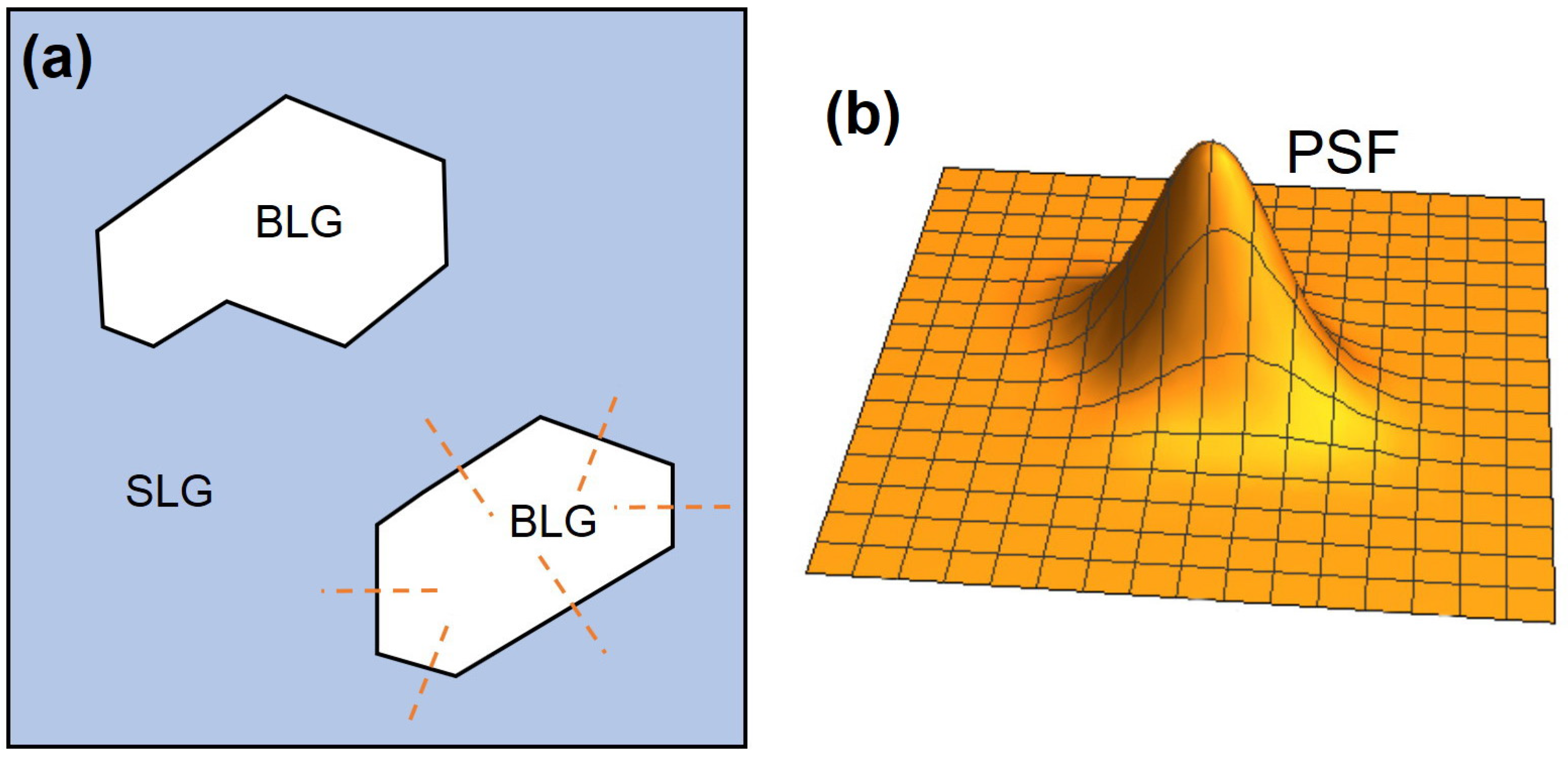
11]. In the case of obtaining SLG film with BLG inclusions in the form of “islands” on the SiC surface, the “islands” with increased potential will appear on the surface potential distribution map of such a structure. These islands of potential will have a rather sharp boundary, which can be used to determine the KPM point spread function. To do this, it is necessary to perform KPM scanning of the island of a BLG island, and then extract the potential cross-section profiles of the potential in different directions (see
Figure 1a). The measured profiles φ
exp(x) are a convolution of the real potential profiles φ(x) (step with a “sharp” boundary) and the KPM point spread function PSF(x) in this direction.
Here, the * sign denotes the operation of convolution of two functions. Let us take the derivative of both parts of Equation (1). The right part of Equation (1) contains the convolution of two functions; that is, the derivative of the convolution of two functions should be taken. We use the following convolution derivative property D(f*g) = Df*g = f*Dg. Here, D means taking a derivative, and the * sign means convolution. This leads to the following expression: φ
exp’(x) = φ’(x)*PSF(x). Then, we use the fact that φ(x) is a “narrow” step; that is, its derivative is a narrow Gaussian-like function similar to the Dirac delta function. The convolution of a function with the Dirac delta function gives the function itself, so we obtain the approximate Equation (2):
Thus, to construct the full PSF, it is necessary to obtain a set of potential profiles at different edges of the BLG potential island (see
Figure 1) and then take the derivatives from these profiles. It should be noted that the PSF does not have to be radially symmetrical for two reasons: (i) the probe axis is inclined to the surface at an angle of 15–25 degrees; (ii) the probe is often not radially symmetrical but may have, for example, a pyramidal shape.
The resulting PSF can then be used to fulfill the deconvolution of the surface potential. To perform the deconvolution procedure, one can use the Gwyddion open-source software [
12].
To accurately measure the PSF, the test sample must satisfy a number of conditions. Layers of the material that differ in the value of the potential must have sharp edges. It should be noted that the SLG/SiC structure with BLG inclusions with the shape of isolated islands satisfies this condition.
On the one hand, the sizes of BLG islands should not be too large. This is necessary in order for the scanned area to contain the entire island, and it would be possible to obtain the necessary set of sections in different directions. It can be assumed that islands with a characteristic lateral size D = 500 nm (and less) are most suitable for measurements. In this case, scanning with the sampling of 512 × 512 points and with a scan step Δ = 2 nm will allow one to measure a whole BLG island and obtain the necessary sections with high accuracy.
On the other hand, the islands of BLG should not be too small. Their lateral sizes should be many times larger than the characteristic lateral resolution of the KPM method. The resolution of the KPM method depends on a number of experimental conditions (probe–sample distance, shape of the probe, radius of curvature of the tip of the probe, etc.) and can be from 30 to 100 nm. It should be noted that there are advanced KPM techniques that allow one to achieve ultra-high spatial resolution (up to the nanometer level). In this paper, we will leave the consideration of advanced KPM techniques beyond the scope, since they require test structures of a different type. Thus, the optimal lateral size of BLG islands for testing the standard KPM method is from 300 to 500 nm.
In addition, BLG islands should be placed on the surface often enough so that there is no need to specifically look for an island on the surface. This means that the surface coating with two-layer graphene should be from 30 to 70%. It also should be noted that the shape of BLG islands on a SiC surface is often very elongated. As a rule, the direction of the “long axis” of islands coincides with the direction of the terraces on the SiC surface [
4]. For a test structure, it is necessary that the islands of BLG are not strongly elongated along a direction, and this requires a special technological regime for growing such samples.
As was shown in one of our previous works [
13], the geometric dimensions of BLG inclusions are related to the surface morphology, which is a set of terraces separated by steps. It was also shown that the parameters of the reconstructed surface (the width of the terraces and the height of the steps) depend on the heating conditions of the SiC substrate. The formation of the graphene/SiC structure occurs in two stages. In the first stage, in the temperature range of 1300–1550 °C, the SiC surface is restructured with the formation of flat terraces separated by steps. This effect is called step bunching [
14]. By varying the heating conditions of the SiC substrate, it is possible to obtain microsteps with step height 0.5–1 nm and macrosteps which consist of a large number of the superimposed microsteps (step height of several nanometers) [
13,
15].
The second stage of graphene formation begins at temperatures above 1600 °C and is accompanied by the decomposition of the terrace surface with the formation of a graphene film. According to [
16], the growth of the second and subsequent graphene layers on the Si-face of SiC substrates is possible only in those places where Si atoms can diffuse from under the first graphene layer to the surface. After the complete coating of the SiC by the SLG surface, there is only one way for the evaporation of Si atoms—through various defects of the graphene layer. In defect areas, BLG formation will be observed. The formation of macrosteps (
Figure 2a) between the terraces results in a break in the graphene film at the edge of the terraces. In this case, the edge of the terrace is the easiest way to continue the formation of the next graphene layer. With such morphology, the BLG surfaces will have the form of continuous longitudinal stripes located along each terrace edge (
Figure 2c). During the formation of the surface of graphene/SiC structures with microsteps (
Figure 2b), a different form of BLG formation is observed. The SLG film in this case has a more perfect structure and does not have breaks at the edges of the steps. The formation of BLG occurs only in separate small areas that have defects in the SLG crystal lattice. In this case, on the surface potential distribution map, BLGs have the form of small islands (
Figure 2d).
Thus, to fabricate a test sample for KPM, it is necessary to grow the graphene/SiC structure with low steps. Such structures, according to one of our previous graphene growth studies [
13], can be formed by setting a relatively low heating rate of the SiC substrate (about 100 °C/min) to a graphene growth temperature of 1730 ± 20 °C.
Since only samples coated with SLG with BLG islands are suitable for using graphene/SiC structures to determine the PSF, we used Raman spectroscopy to analyze the structure and thickness of our graphene. The Raman map and typical Raman spectra of the test sample in the region of the 2D line are demonstrated in
Figure 3a,b, respectively. Both Raman spectra demonstrate features characteristic of high-quality graphene grown on 4H-SiC substrate: G and 2D lines and a contribution of the buffer layer [
17]. The absence of the defect-related D-line points to the defect-free nature of the graphene film.
As can be seen in
Figure 3b, the 2D line in the spectra obtained from dark areas in
Figure 3a (p. 1) has a symmetric Lorentzian shape, typical for SLG. However, in the yellow areas (p. 2), the 2D line has a clearly asymmetric shape with a pronounced low-frequency shoulder, which can be fitted with four Lorentzians. The splitting of the 2D line into four components is characteristic of BLG with AB stacking, the Dirac cone of which splits into two subbands, enabling four Raman-active scattering routes with different resulting frequencies [
18]. Thus, we can state that the red spectrum from
Figure 3b and hence the yellow areas in
Figure 3a correspond to AB-stacked bilayer graphene [
19].
Figure 4a shows a KPM image of the proposed test graphene/SiC sample containing BLG islands ranging in size from 300 nm to 1000 nm. The images of the edges of the bilayer graphene regions are “blurred” by the width of the PSF function, so they do not look sharp in the given image (
Figure 4a). The main idea of this paper is that from this “blurring” of the edges we extract information about the width of the PSF function. The distance between BLG islands is comparable to their characteristic sizes (BLG surface coverage is about 30%), which makes it easy to detect an island of the desired size almost anywhere in the sample. By extracting profiles along different directions at the edges of the islands, one can then construct a PSF, an example of which is shown in
Figure 4b. The resulting PSF has an approximately bell-shaped form, and its characteristic width is about L = 70 nm. This value of L is the lateral resolution of the KPM method for a given probe and given scanning conditions. In general,
Figure 4 shows the implementation of the conceptual scheme from
Figure 1.
The resulting PSF can be used to restore the exact value of the measured KPM potential. For this purpose, the procedure of deconvolution of the measured KPM potential with an instrumental function is used.
Figure 5a shows the experimentally obtained image of KPM, and the image on the right in
Figure 5b shows the image obtained after the deconvolution procedure. It can be seen that the boundaries of the islands in the original image are slightly blurred, while these boundaries have become sharper in the image after deconvolution.
Figure 5c compares the potential profiles from the original KPM image (black profile) and from the deconvoluted KPM image (red profile). The approximate location where the profiles were taken is marked with arrows in
Figure 5a,b. It can be seen that the deconvolution of the original image with the point spread function leads to some decrease in the lateral sizes of the measured features. In
Figure 5c, such places are marked with arrows. The characteristic noise when measuring the potential in our measurements is approximately 2–3 mV. This is several times less (in some places, an order of magnitude smaller) than the observed differences shown in
Figure 5c. For example, at x = 0.8 µm (see
Figure 5c), the potential difference (after deconvolution) is 30 mV. The resulting difference is significant when compared to the noise level. In addition, the peaks of the measured potential features in the original image correspond to smaller values compared to the values obtained after deconvolution. For example, in the left part of the profile, the value of the potential step on two-layer graphene after deconvolution approached the value of 0.13 V, which is the true value of the potential for this case. This is due to the fact that during the experimental measurement of the potential, the influence of the PSF leads to a decrease in the measured values of the potential and a broadening of the measured features. This problem can be partly solved by measuring the PSF and performing the deconvolution procedure. It should also be noted that our procedure for extracting the PSF and further deconvolution of the KPM potential affected only the surface potential data; the topography data were not perturbed (see
Figure S1 in
Supplementary Information).
Several groups previously performed studies on obtaining PSF for Kelvin probe microscopy. T. Machleidt et al. [
3] and G. Cohen et al. [
20] obtained PSF for KPM, but this was done in a different way. To obtain the PSF function, an analytical calculation of the electrostatic interaction of the probe with the surface was performed, while it was necessary to accurately know the geometric shape of the probe tip. The shape of the probe tip was determined experimentally by scanning test surfaces with sharp needles (TGT1, NTMDT). It is worth noting two shortcomings of the T. Machleidt method: (i) the need to scan a very rough surface with sharp needles, while there is a high probability of damage to the probe tip; (ii) the shape of the probe beyond the tip part being poorly taken into account. The electrostatic interaction of the SPM probe with the surface is a long-range one, so it is necessary to accurately take into account the contribution from the probe beyond the tip part (pyramid of the probe). In our method, firstly, there is no need to scan a very rough surface with needles, and secondly, since the PSF is extracted from the experimental KPM data on the test surface, all contributions to the interaction are taken into account automatically.


 ,
, 


