Article

Robust Packaging of Vertically Aligned Graphite Substrate by Copper Micro-Rib Structuring

1
Surface Engineering Design Laboratory, Shibaura Institute of Technology, Tokyo 144-0045, Japan
2
Ebina Denka Kogyo, Co., Ltd., Tokyo 144-0033, Japan
3
Thermo-Graphitics, Co., Ltd., Osaka 551-0032, Japan
*
Author to whom correspondence should be addressed.
Submission received: 12 October 2022 / Revised: 13 November 2022 / Accepted: 21 November 2022 / Published: 28 November 2022
(This article belongs to the Topic Application of Graphene-Based Materials)

Abstract

:
Vertically aligned graphite substrate (VGS)-copper packaging was renowned for improving the robustness against the thermal gradient loading by using micro texturing. The micro-groove array with a line width of 50 μm and a pitch of 100 μm was formed into the VGS by controlling the line depth with the use of fast-rate oxygen plasma etching. Three micro-grooved VGS specimens were wet-plated to fill these microgrooves with copper deposits and to cover the VGS surfaces. The nearly full-deposited VGS-Copper specimens were subjected to a severe thermal transient loading test. The simply Cu-covered package and shallow rib-structured VGS-Cu packages were damaged to delaminate at their interfaces. The VGS-Cu package with the copper rib structure with a height of 50 μm experienced no delamination. This rib-structured VGS-copper package with high rib height had sufficient robustness against the severe thermal transients even with the proof of homogeneous thermal spreading capacity.

1. Introduction

Since the first studies on the application of massive MIMO (Multi-Input Multi-Output) GaN power device [1,2], it has been attracted as a base bureau for mobile phone communication. Most of the GaN FET (Field Effect Transistor) in this arrayed system was down-sized or power-moduled for improvement of efficiency instead of Si-based FET [3]. In order to save the demerits of GaN FET, many studies were reported on the improvement of the reliability of hollowed GaN chips and their thermal spreading and transient capacity [4]. The LCP (Liquid Crystal Plastics) was utilized for hollowed packages to demonstrate their gross-leak proof [5,6]. The micro-textured packaging method was also proposed to improve the leak-proof of packages [7]. However, the thermal dissipation process in the package is still complicated and difficult to aim at high thermal spreading capacity, as reported in [8]. The first approach was a multi-layer package with a stack of several materials. In particular, the graphene sheet package [9] and the multi-stacked graphene packaging [10] were highlighted to make full use of their high electrical and thermal conductivity. A single- and multi-VGS (Vertically-aligned Graphitic Substrate) with copper coverage was also developed to promote a higher heat-spreading capacity [7]. Those candidate packages have been revised to have sufficient robustness to be working under severe thermal transients [11].
In the VGS-packaging design, the generated heat by GaN chips in working is efficiently spread to the cooling device through VGS with its highest thermal conductivity [12]. As discussed in [5,13], this thermally spreading process advances homogeneously to leave no hot spots in the GaN chips and in the VGS, even during severe thermal transients due to the single-/multi-VGS substrate structure. However, the thermal strain is induced in the copper layer by the difference in thermal expansion coefficients between the copper layer and VGS. An expected VGS package has sufficient structural integrity and robustness to be free from risk of delamination on the interface between the copper layer and the VGS and homogeneous thermal spreading performance through the copper coverage without thermal gap conductance on the VGS and copper interface.
In the present paper, the micro-textured VGS-copper package design is proposed to homogenize the thermal spreading behavior from the heated GaN chips and to improve the mechanical integrity and robustness as a total package system even during severe thermal transients. After [14,15,16,17], the tailored microtexture in the two-dimensional topology is formed into VGS by using the high-intensity oxygen plasma etching. The plasma diagnosis with the aid of EOS (Emissive-light Optical Spectroscopy) is used to monitor the reaction of an activated oxygen atom from plasmas to the carbon in VGS after [18]. The Raman spectroscopy and four-terminal method are utilized to prove that no damages and defects are significantly introduced into VGS by oxygen plasma etching. After cleansing and polishing, the wet-plating is used to fill the micro-groove array in VGS with copper deposits and to form the rib-structured VGS-copper package specimens. Through the thermal shock test, where the heated package is quickly placed onto the cold bed, the rib-structured package with more rib height than 50 μm has sufficient robustness to be free from delamination on the package interface.

2. Materials and Methods

Thick graphene solid was first synthesized by the thermal CVD (Chemical Vapor Deposition; Thermotech, Co., Ltd., Dallas, TX, USA) method as a feedstock. This solid feedstock was machined and sliced to a VGS substrate as specimens in the following experiments. A new VGS-packaging design is proposed to prevent the copper-VGS package from interfacial delamination on the interface between the copper layer and the VGS by rib-structuring. The microgroove array in VGS is filled by the copper deposits to form the rib-structured copper coverage on VGS and prepare the package specimens for thermal shock test. SEM (Scanning Electron Microscopy), LM (Laser Microscopy), and three-dimensional profilometers were utilized to describe the plasma etching and wet-plating processes.

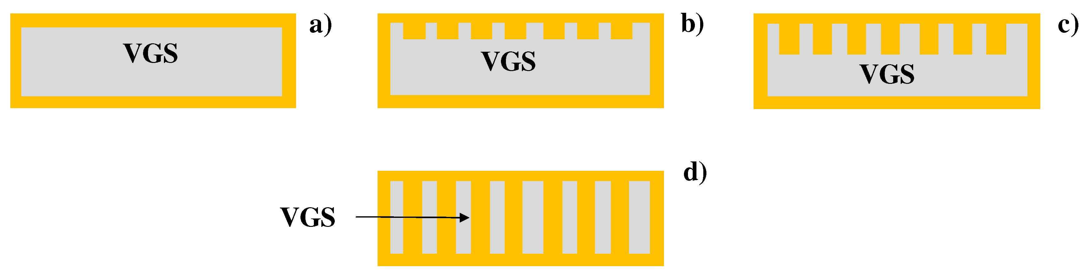
2.1. Graphene Base Packaging Design

Four types of vertically-aligned graphene substrate (VGS) packages were considered to search for an optimum system with robustness in structural integrity. The simply covered VGS substrate in Figure 1a was utilized as a reference; the copper layer delaminates by the thermal strain (ε) or ε = (αCu − αVGS) × ΔT where αCu and αVGS are the thermal expansion coefficient of copper and VGS, respectively, and ΔT is a thermal gap between the package and the cold bed. Two rib-structured VGS-copper packages in Figure 1b,c were prepared to have an array of copper rib members into VGS. The effect of copper rib height on the thermal transient response is investigated to optimize the rib-structured package geometry with sufficient robustness against the thermal transient loading.
Figure 1d depicts an extreme design for copper rib-structured packages with increasing the rib-height. In this extreme package design, the copper micro-columns through VGS combined with copper coverage on the VGS surfaces. In the first step, three specimens in Figure 1a-c were prepared in the following experiments to demonstrate the validity of this packaging design strategy.

2.2. Microtexturing onto VGS Surface by Screen Prining

The screen printer (Newlong; Tokyo, Japan) was utilized to print the negative micro-pattern as a line-segment array onto the VGS specimens with the use of water-soluble ink. Figure 2 depicts a typical line-segment array, where the unprinted lines have a uniform width of 50 μm and pitch of 100 μm.

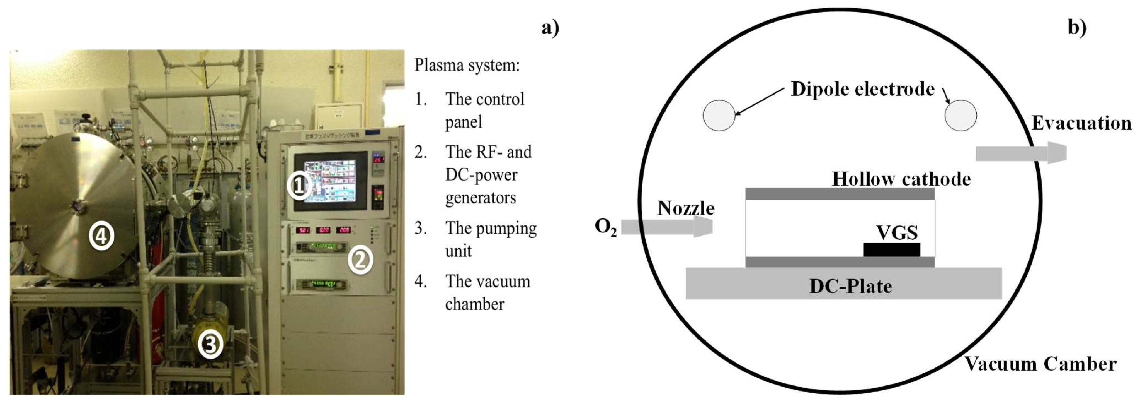
2.3. Plasma Etching of VGS

A plasma oxidation etching process (YS-Electric Industry, Kofu, Japan) was utilized to shape a micro-groove array into VGS specimens. As depicted in Figure 3a, the oxygen plasma was driven by the RF (Radio-Frequency) and DC (Direct Current) generators at the specified pressure.
The hollow cathode setup was utilized to densify the population of activated oxygen ions and activated atoms, as depicted in Figure 3b. As recently reviewed in [19], the hollow cathode discharging process was effective in attaining the high-intensity oxygen plasma state. This hollow cathode device was placed between the dipole electrodes to confine the generated RF-plasmas into a hollow after [13,14,15]. The plasma diagnosis using the EOS (Hamamatsu Photonics; Hamamatsu, Japan) was utilized to certify the high density of activated oxygen atom species in the hollow cathode device. The targeting measurement spot was focused in the vicinity of the VGS specimen, away from the outlet of gas flow by 2 cm in Figure 3b. Figure 4 depicts the measured spectrum of ignited oxygen plasma under the RF voltage of 250 V, the DC bias by −500 V, and the oxygen gas pressure of 50 Pa. The two highest peaks corresponded to OI profiles or activated neutral oxygen atoms. The oxygen plasm etching advanced by the in situ reaction between the activated oxygen atoms from this high-density plasma and the carbon from VGS in a similar manner to the plasma chemical reactions during the plasma oxygen etching of DLC (Diamond Like Carbon) films [13,14], the diamond coating [15], and the graphite and VGS solids [16,17].
In the following etching experiments, the plasma conditions with 250 V for RF-voltage and −500 V for DC-bias were employed as a standard condition. The pressure for oxygen gas flow was varied by P = 50 Pa, 70 Pa, and 100 Pa to investigate the effect of plasma oxidation conditions on the quality of micro-grooved VGS.

2.4. Copper Wet-Plasting

After chemically polishing and cleansing the plasma-printed VGS specimen, the normal wet-plating method was utilized to wrap three micro-grooved specimens. The average copper coverage thickness was 45 μm. Different from the brazing method [20], the copper deposition advanced in the ionized solution. This copper wet-plating method was free from oxidation and thermal damage during the copper deposition process.

2.5. Thermal Transient Testing

Each VGS-Cu package specimen was placed onto the hot plate and heated up to 573 K. After holding it for 300 s, it was rapidly cooled down on the cold bed at RT.
The texting procedure is depicted in Figure 5. A normal VGS-Cu package specimen with shallow copper rib height was tested by this setup to certify that it was severely damaged with complete delamination of the copper layer from VGS. After [21], the thermal gap was estimated to be changed by 30 K/s in the early stage of cooling. At this cooling rate, the specimen was subjected to severe thermal shock.

3. Results

VGS specimens were plasma-etched to form microgrooves on their top surface. The micro-grooved VGS was analyzed by SEM, and Raman spectroscopy and measured by the four-terminal method and laser microscopy. The rib-structured VGS-Cu packages were fabricated by wet-plating. They were also measured by laser-microscopy. The thermal transient loading test was employed to analyze the effect of copper rib structure on the mechanical robustness against the thermal shock.

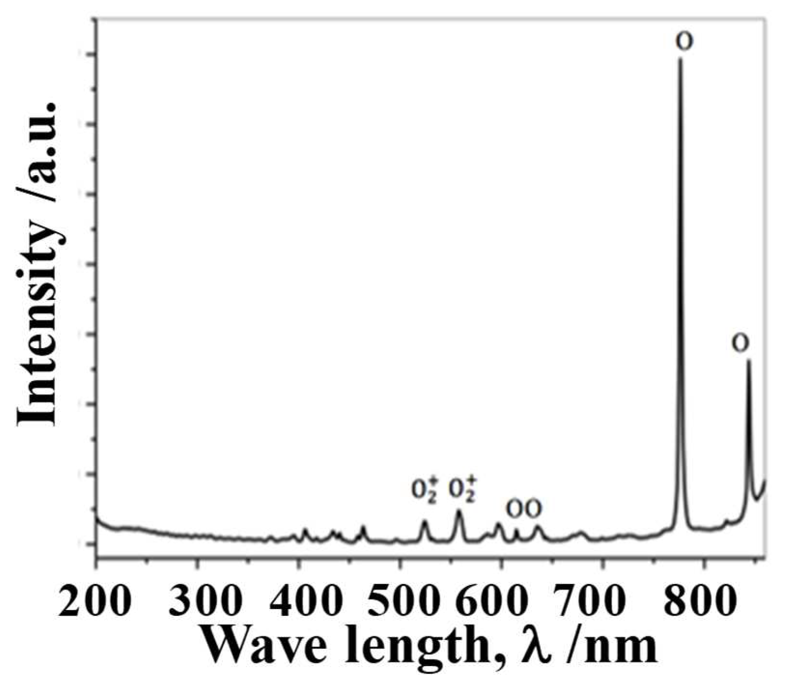
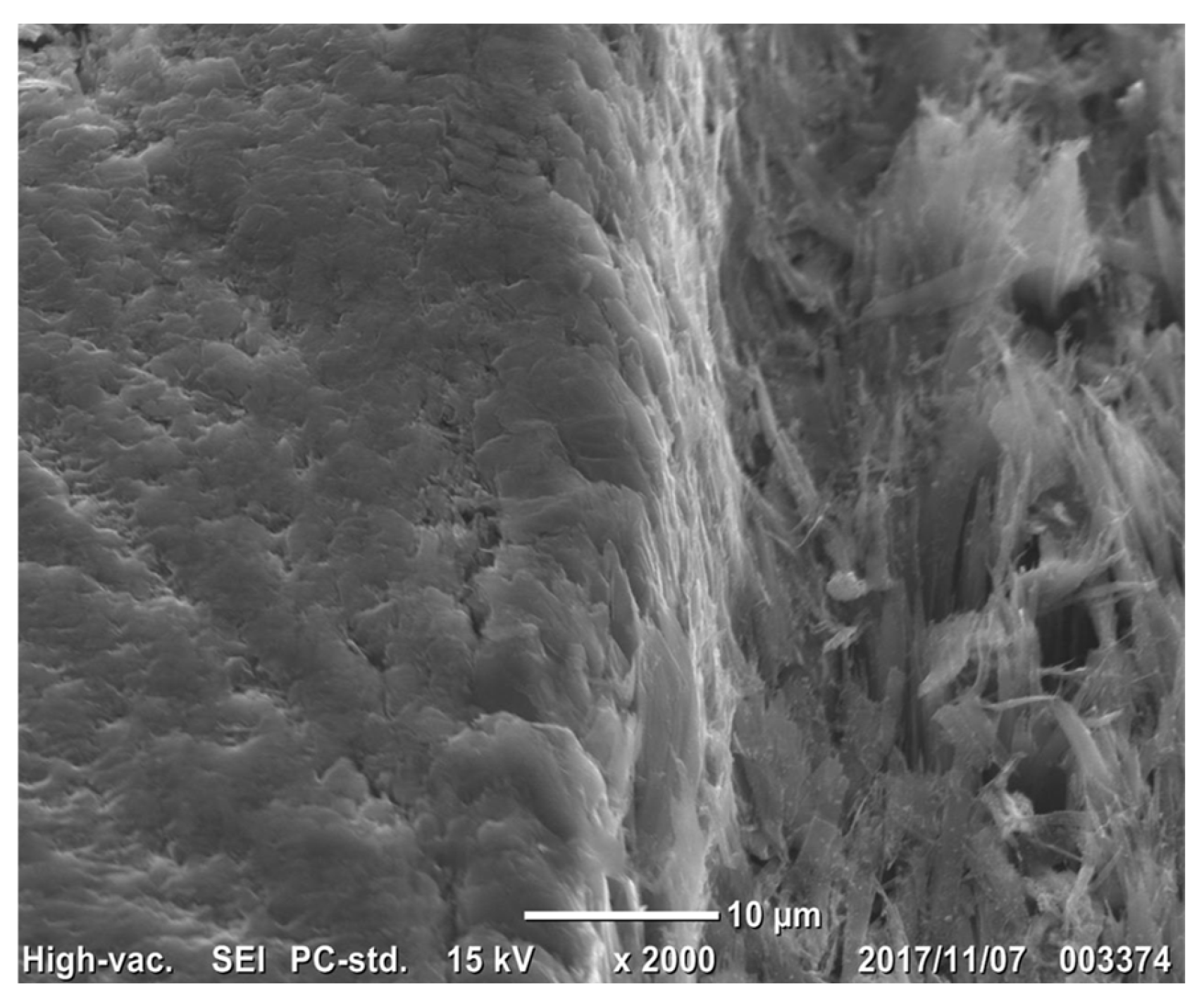
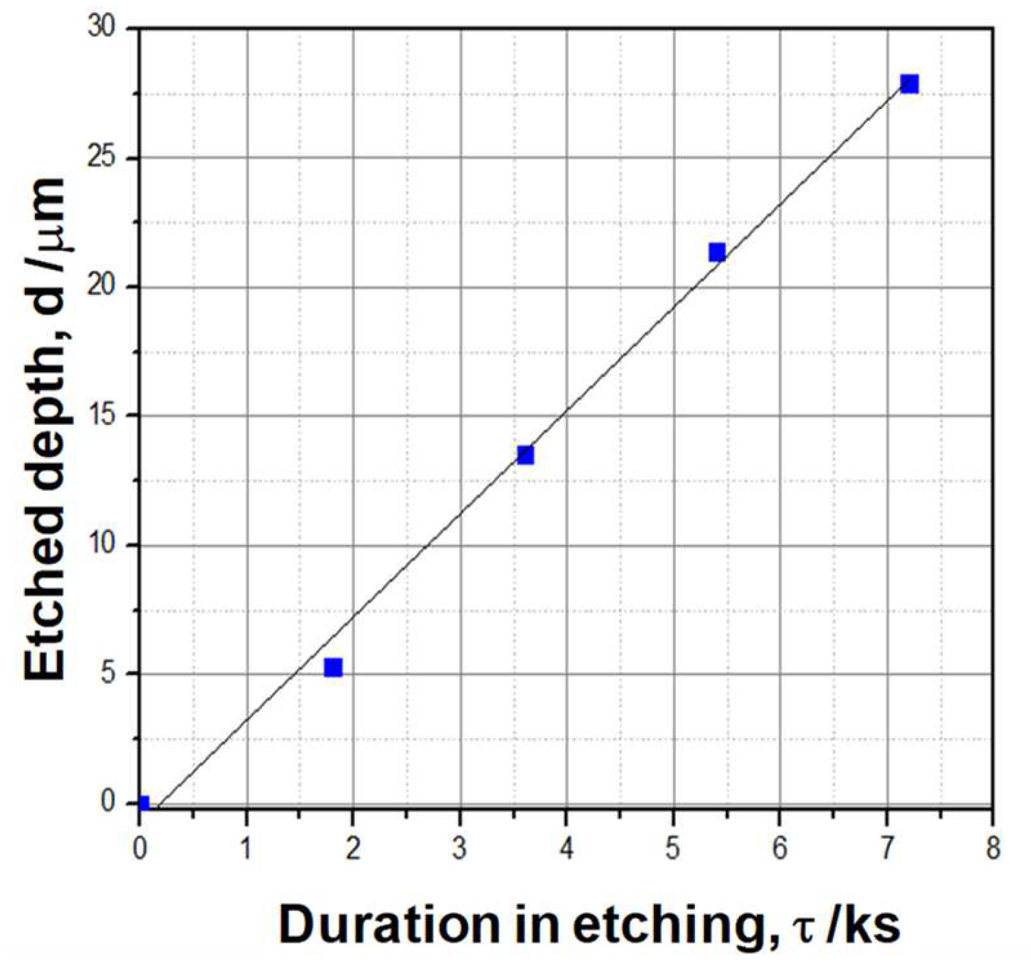
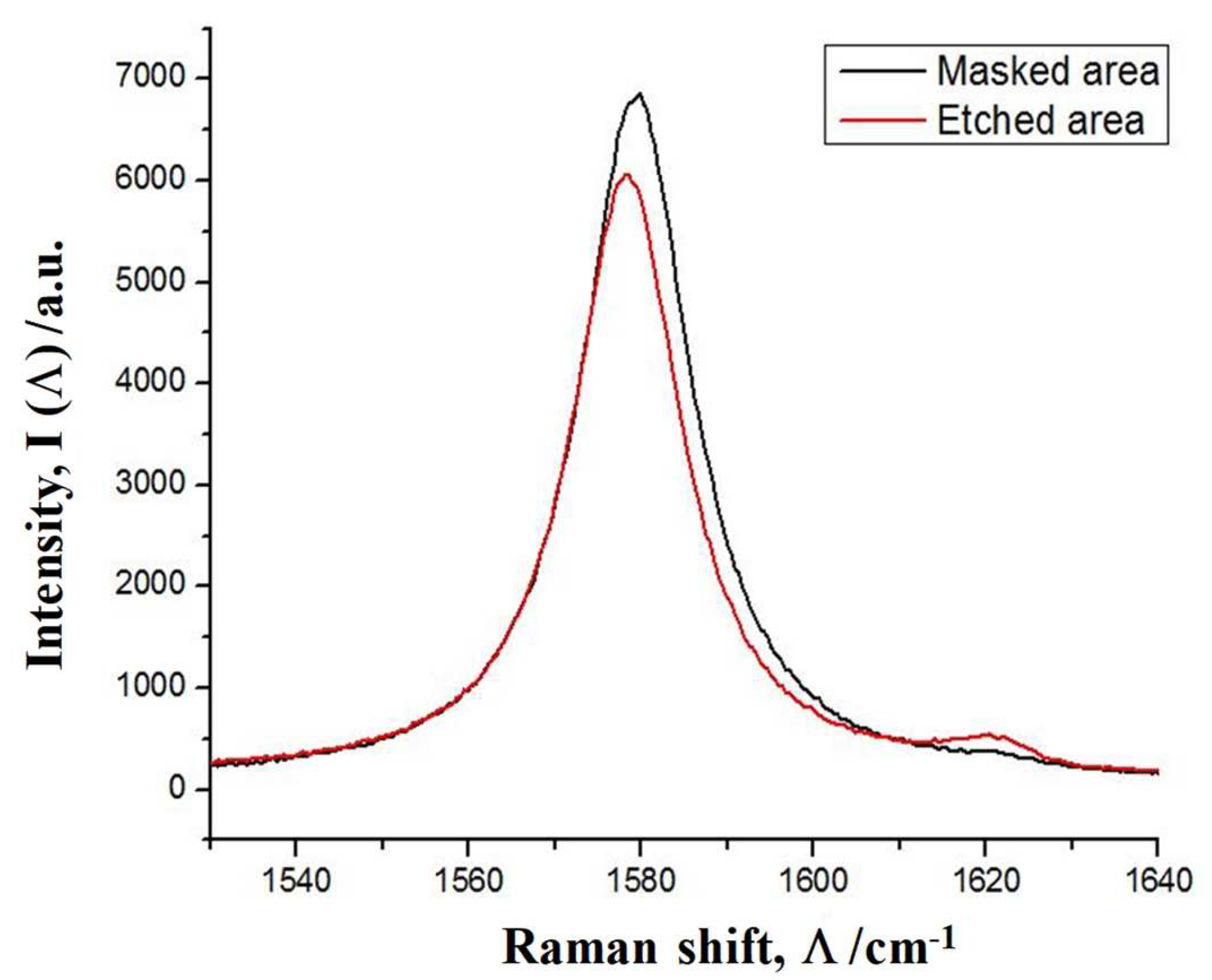
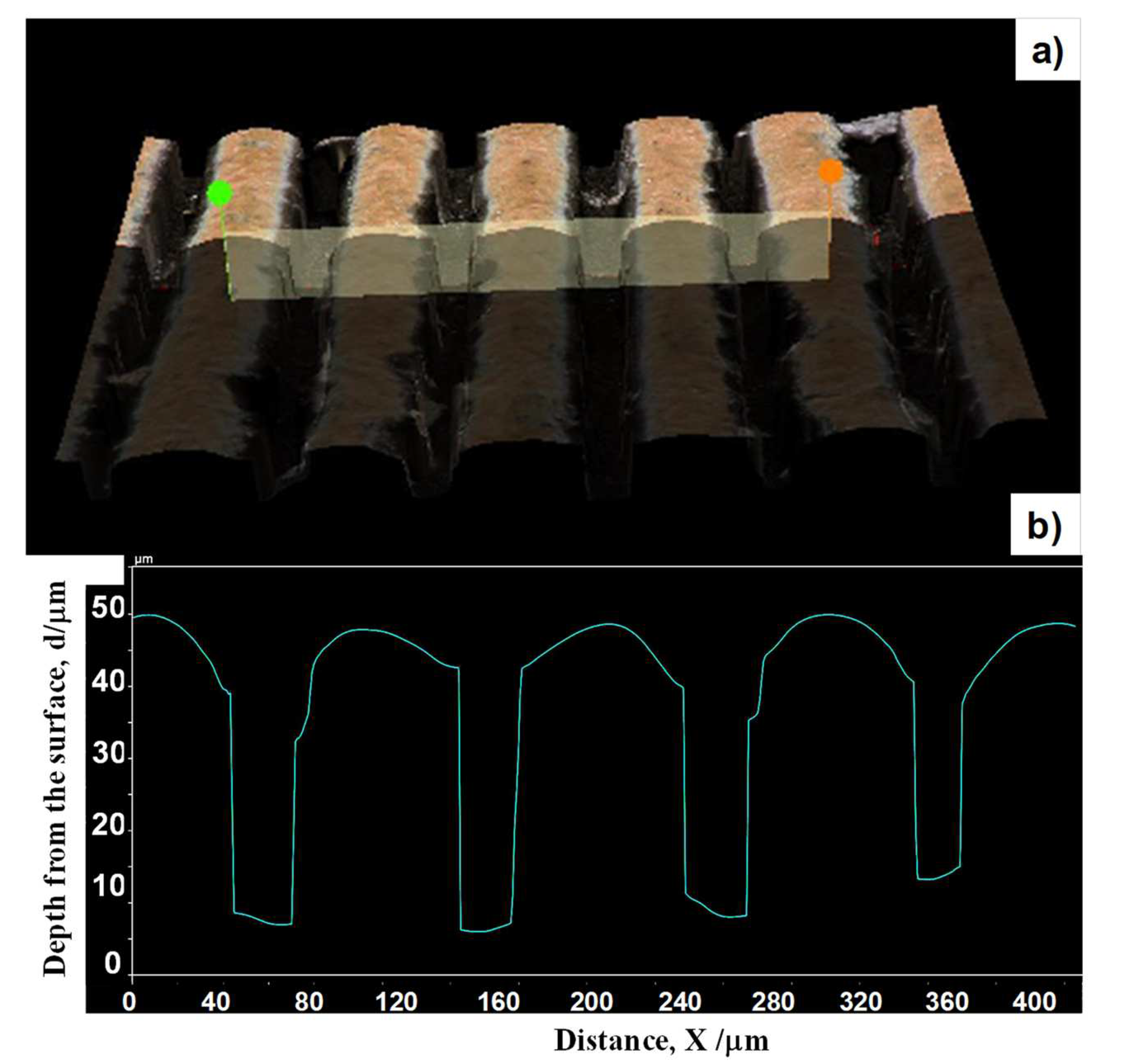
3.1. Oxyegn Plasma Etching of VGS

Figure 6 depicts the SEM image on the VGS specimen after the etching process for 7.2 ks. As estimated in Figure 4, this oxygen plasma etching process is driven by the in situ chemical reactions via C (in VGS) + O (in plasmas) → CO in addition to the physical ion bombardment of the ionized oxygen molecules. Since CO gas was ejected out of the system, this reaction advanced with increasing time.
The duration (τ) was varied in order to investigate the average etching rate in this oxygen plasma processing. The RF-voltage, the DC bias, and the pressure were held constant in every etching process. Figure 7 depicts the variation of the etched depth with increasing τ. The etching depth increases monotonously with the etching duration; e.g., d = 5 μm at τ = 1.8 ks, and d = 26 μm at τ = 7.2 ks. This monotonous etching behavior implied that the oxygen plasma etching homogeneously advanced only into the depth of unmasked VGS. The average etching rate is estimated to be 4 μm/ks or 13 μm/h. How to improve this etching rate is discussed later with reference to the previous studies in the literature.
Raman spectroscopy was utilized to investigate the difference in the VGS surface structures before and after the etching process. Figure 8 compared the Raman spectra of VGS surfaces before and after the oxygen plasma etching, using the excitation laser with a wave length of 532 nm. The Raman shift range was specified from 1530 cm−1 to 1640 cm−1. The typical graphitic peak was detected at 1579 cm−1 before etching and at 1578 cm−1 after etching, respectively. No difference is detected in the G-band; the typical sp2-vibration mode is common to these two measurements. To be noticed the G′ band or the disordered G-band is also detected as a shoulder at 1620 cm−1 after etching. This is just corresponding to a structural disorder in the sp2 structure, as reported in [22]. This structural disorder might be induced by the plasma oxidation process in the vicinity of etched edges between masked and unmasked VGS surfaces.
Structural disordering has a possibility to affect the thermal and electrical conductivities of VGS [23]. The four-terminal method was utilized to measure the electric resistivity (ρ) both on the masked and etched surfaces. Since ρmasked = 1.17 × 10⁻³ Ωcm in the masked VGS and ρetched = 1.24 × 10⁻³ Ωcm in the etched VGS, no significant difference was detected in electric resistivity. As stated in [24], the free electrons could be easily trapped by the defects and edges in the processed VGS to increase the electric resistivity up to ρ20 = 5 × 10⁻³ Ωcm. Since ρmasked ~ ρetched < ρ20, the disordering effect by the plasma oxidation on the electric properties is too small to deteriorate the intrinsic properties of VGS by the micro-grooving process.

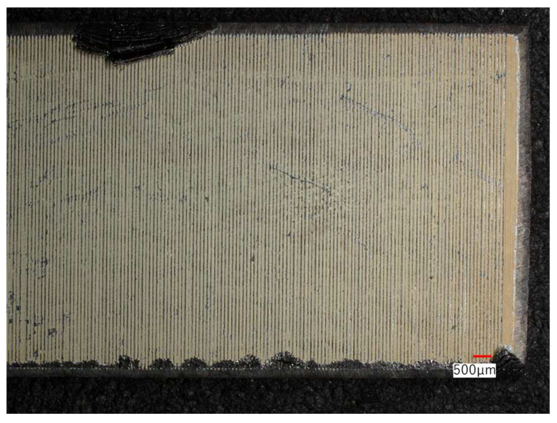
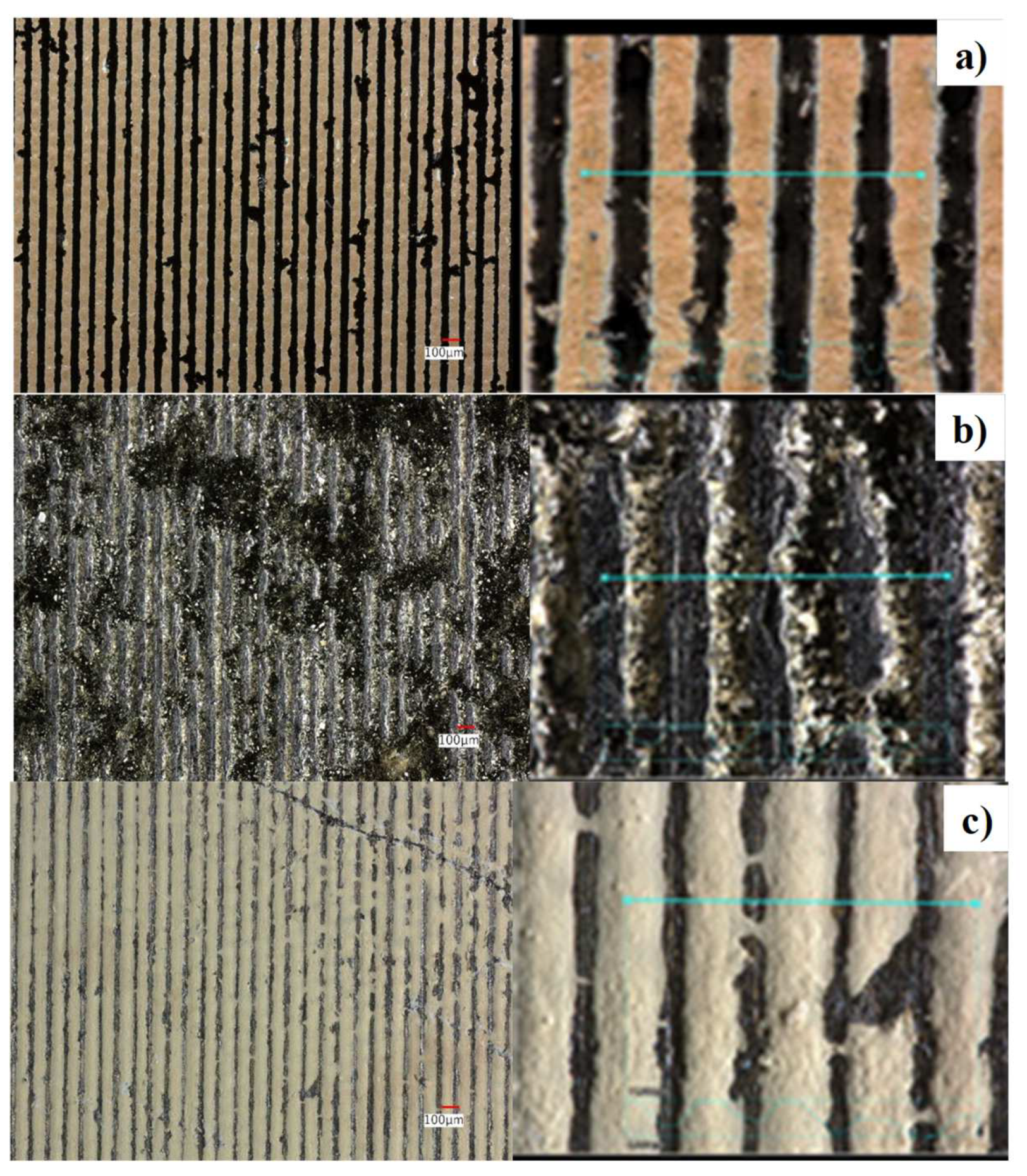
3.2. Fabrication of Micro-Grooved VGS Specimen

The oxygen plasma processing was utilized to fabricate the micro-grooved VGS specimens. Three VGS specimens with different micro-grooves were yielded by oxygen plasma printing. Figure 9 depicts three micro-grooved VGS specimens before chemically polishing and cleansing.
The depth of microgrooves in these three VGS specimens was measured by laser microscopy. Figure 10 depicts the cross-section of the VGS-1 specimen in Figure 9a. The straight micro-grooves with a width of 25 μm and a lateral length of 10 mm were regularly shaped into the VGS.
As had been reported in [13], each microgroove depth (d) was nearly constant in each plasma etched VGS specimen with a pitch of 100 μm. As depicted in Figure 9a, this VGS-1 specimen has the deepest micro-groove array with d = 50 μm. The VGS-2 in Figure 9b has a shallower micro-groove with d = 45 μm than that in Figure 9a. The VGS-3 in Figure 9c has the shallowest micro-groove, e.g., d = 7 μm. These three micro-grooved VGS specimens were wet-plated under the same processing conditions after chemically polishing and cleansing them.

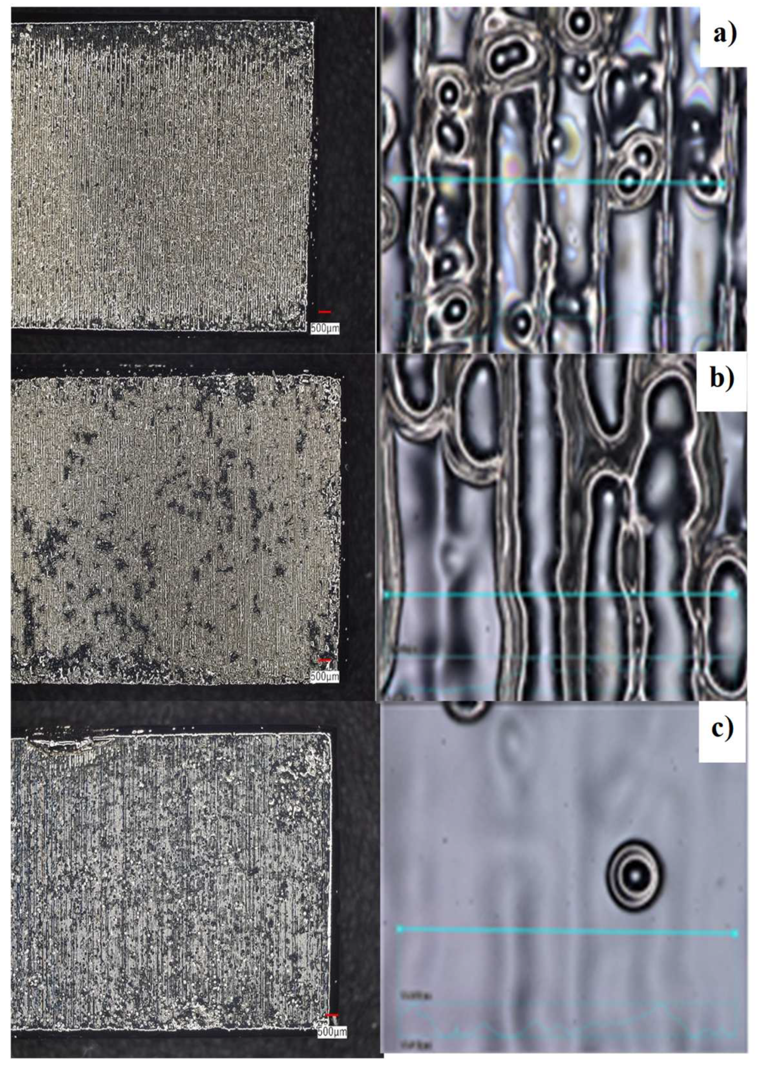
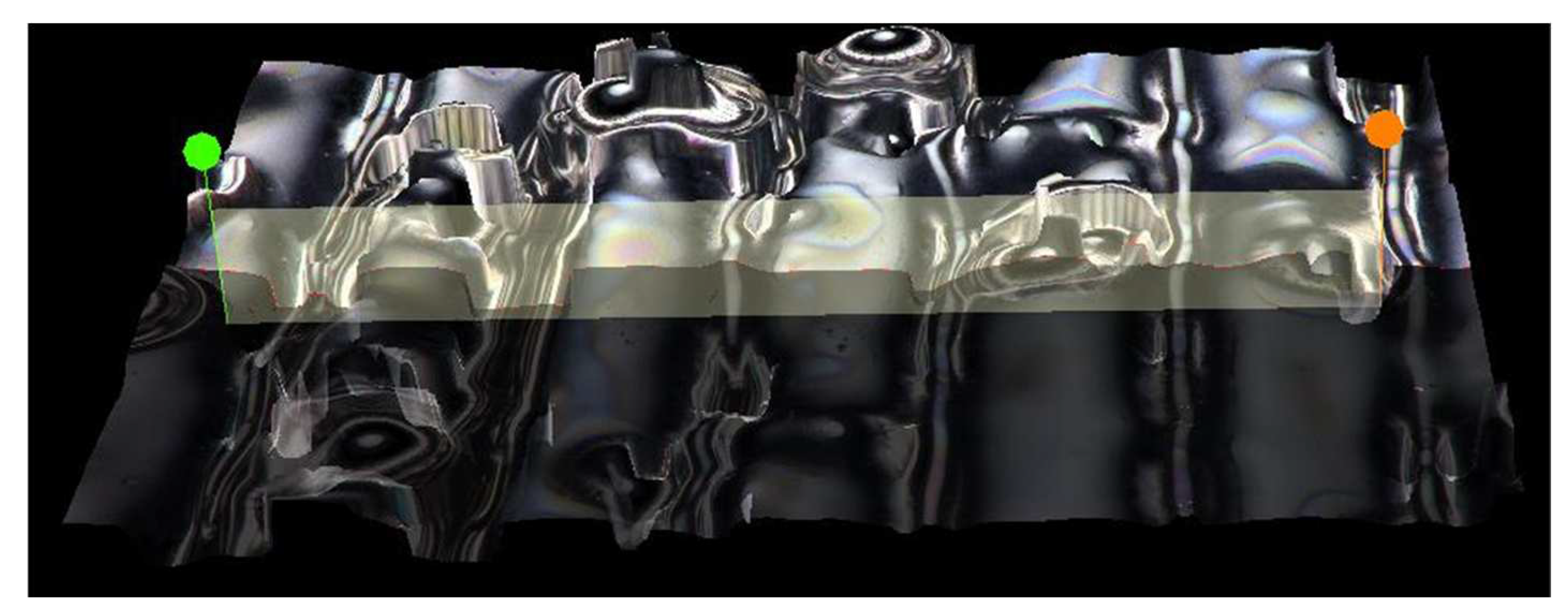
3.3. Fabrication of VGS-Copper Package

The VGS-Cu packages were fabricated and analyzed by SEM and laser microscopy. Figure 11 compares the surface morphology among three packages. As depicted in Figure 11a, the copper ions dipped into the depth of microgrooves, and the whole micro-grooved VGS surface was covered by copper. The maximum roughness (Rmax) was measured to describe the filling process into micro-grooves by this wet-plating; in the case of Figure 11a, Rmax = 15 μm. To be discussed later, some microgrooves remained not to be fully filled by copper.
The measured Rmax was 45 μm for the specimen in Figure 11b with d = 45 μm, and Rmax was 7 μm in Figure 11c with d = 7 μm. This revealed that the completely unfilled microgrooves by copper were left in the VGS-2 and VGS-3 specimens. This unfilling state came from the fall-down of microwalls between adjacent microgrooves during the plasma oxidation. That is, d > Rmax in Figure 11a proves that the micro-groove arrayed VGS is filled by a copper layer without any unfilled state. The copper deposition and filling process into microgrooves were investigated for the package in Figure 11a. Figure 12 depicts the surface profile of the VGS-Cu package in Figure 11a. Although some microgrooves without a fully filling state were detected by this microscopic laser measurement, most the microgrooves were fully filled to form a relatively smooth surface. The deep microgroove array in this VGS-1 with stiff micro-walls was near-fully filled by the copper deposits during the wet-plating to be free from surface damage.

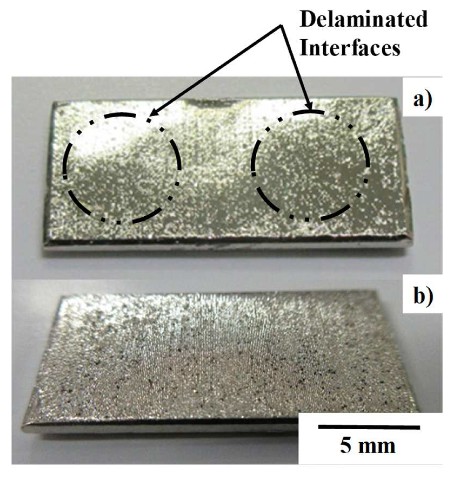
3.4. Thermal Transient Loading Test

Three VGS-Cu packages with different copper rib structures were subjected to the thermal shock test. Figure 13a depicts the surface profile of the VGS-Cu package in Figure 11c after the thermal shock test with the thermal gap of 300 K between the package and the cold bed. Most of the copper coverage is delaminated by itself due to the thermally induced strains on the interface between VGS and copper coverage. Considering that the thermal strain is estimated by ε ~ αCu × ΔT = 17.8 × 10⁻⁶/K × 300 K = 0.5% for αVGS ~ 0, the shallow copper rib structure is pulled out from the microgrooves in VGS by this thermal strain. On the other hand, as shown in Figure 13b, no delamination was observed on the surface profile of VGS-Cu packages in Figure 11a. The original surface profile in Figure 12 was preserved even after the thermal transient testing. This demonstrates that the copper rib structure with sufficient rib height into the VGS substrate has enough robustness and toughness never to delaminate by itself, even under severe thermal transients in practice.
Let us consider the effect of micro-groove geometry on the resistance against the thermal shock test. By narrowing the pitch and width of microgrooves and deepening the micro-groove cavity, the mechanical anchoring effect is enhanced to reduce the tensile thermal stress on the interface between the micro-grooved VGS and the deposited copper layer. The topological structure design [25] is needed to optimize the mechanical anchoring effect on the delamination-free interface and to homogenize the thermal conductivity across the thickness of the VGS-copper package.

4. Discussion

As had been discussed in [17], the etching rate (E) of carbon base solids by plasma oxidation is strongly dependent on their microstructure in addition to the plasma conditions. E = 6 μm/h for PVD-DLC film, E = 90 μm/h for CNT, E = 6–8 μm/h for thick CVD-DLC film, and E was 13 μm/h for VGS in the present study. This relatively fast rate etching is attributed to the sp2-structured graphene structure in VGS. When using this etching process for the micro-grooving treatment of VGS, a much faster etching rate is needed to form deeper micro-groove structures. In addition to the improvement of the etching rate, the integrity of the micro-groove arrayed VGS must be preserved through the etching process. As seen in Figure 9b, the microgroove walls were damaged by the severe bombardment of oxygen atoms. When increasing the gas pressure up to 100 Pa, this bombardment damage to the walls was significantly reduced, as depicted in Figure 9a and Figure 10. These homogeneously formed microgrooves reflect on the copper deposition and filling process to shape the copper rib structures with taller rib heights.
As shown in Figure 11a and Figure 12, the Cu-deposition and filling process into microgrooves in VGS forms a relatively uniform package surface with lower Rmax. In order to further reduce this Rmax, the electric field in the wet plating operation is optimized to reduce the deviation of Cu deposits. In addition, the ionized flow control in the bath for wet-plating is also necessary to accelerate the copper deposition into micro-grooves.
The copper rib structure with sufficient rib height in the VGS-Cu package is responsible for structural integrity without interfacial delamination against severe thermal transient loading. Let us consider this mechanical anchoring effect of the Cu-rib structure. The simple Cu layer on the VGS without rib structures is pulled up from the VGS-Cu interface by the tensile thermal strain (ε). In the presence of the Cu-rib structure, the Cu-columnar ribs in VGS pull back the Cu-layer against the pulling-up strain to prevent the Cu-layer from delamination. This pulling-back strain increases with increasing the Cu-rib height so that no delamination occurs in the VGS-1-Cu package.
In addition to the mechanical robustness of the rib-structured VGS-Cu package, this package design is preferable to promote the thermal spreading capacity. As partially stated in [7], the channel temperature (Tch) and resistivity (ρch) were much more reduced in the VGS-Cu substrate than in the copper-based composite substrate even when they had the same substrate thickness; e.g., Tch = 147 °C and ρch = 0.79 °C/W in the VGS-Cu substrate while Tch = 189 °C and ρch = 1.1 °C/W in the composite. This capacity was often deteriorated by the interfacial flaws, which were induced by the thermal transients. The robust integrity of rib structuring also preserves the thermal spreading capacity even after the thermal transient test.
As suggested in [26], the interaction between the VGS and the copper crystals on the interface often plays a role in the mechanical properties and in the thermal spreading performance. In different from the interface between the graphite and the brazed copper [27], no oxidation occurs during the copper deposition by the wet-plating. The present wet-plating has a possibility of a chemical reaction between the graphene planes in VGS and the deposited copper crystals in the preferable orientations. Further studies by XPS are necessary on the interfacial interaction between the VGS and the wet-plated copper.
In the present study, the copper rib-structure ends were terminated in the middle of VGS thickness in preparation for VGS-Cu package specimens. As their extreme case in Figure 1d, when the Cu-rib columns are formed through the VGS thickness, the thermal conductivity (κ) of packages is also controlled together with mechanical robustness. After [28], κthick along the graphitic VGS thickness is nearly equal to κCu while κsurface along its surface is a little smaller than κgraphene. When using the graphene-like VGS, κthick ~ κgraphene and κsurface–κCu. This suggests that VGS structure, used in [7,13], is simplified to validate its thermal spreading capacity in the VGS-Cu packaging design without loss of robustness in the mechanical integrity.

5. Conclusions

The rib-structured VGS-copper package was proposed to preserve mechanical integrity with robustness against thermal transient loading. Two-step procedure was proposed for this copper rib-structuring; the micro-grooving of VGS by oxygen plasma etching and the copper wet-plating. The plasma etching condition was determined by the plasma diagnosis; the normal etching rate was attained by 13. 4 μm/h. Three VGS-copper package specimens with different copper rib structures were prepared for the thermal loading test. The micro-grooved textures formed by oxygen plasma etching by 100 Pa provide the highest rib-structure of 50 μm enough to prevent the copper layer from delamination from VGS even under severe thermal shock test. This robustness comes from the mechanical anchoring of copper rib structures into the micro-grooves of VGS.

Author Contributions

Conceptualization, T.A. and Y.N.; methodology, T.A., H.N. and T.N.; software, H.N. and T.N.; validation, T.A., H.N. and T.N.; formal analysis, T.A. and T.N.; investigation, T.A., H.N. and T.N.; resources, Y.N.; data curation, H.N. and Y.N.; writing—original draft preparation, T.A.; writing—review and editing, T.A., H.N.; visualization, H.N. and T.N.; supervision, Y.N.; project administration, T.A. and Y.N. All authors have read and agreed to the published version of the manuscript.

Funding

This research received no external funding.

Acknowledgments

The authors would like to express their gratitude to Kurozumi S-I. (Nano-Film Coat, llc.) for his help in the thermal transient loading test.

Conflicts of Interest

The authors declare no conflict of interest.

References

  1. Schnaufer, D.; Peterson, B. Gallium Nitride—A Critical Technology for 5G; Qorvo White Paper: Chandler, AZ, USA, 2016. [Google Scholar]
  2. Doughetty, D.; Mahalingam, M.; Viswanathan, V.; Zimmerman, M. Multi-lead organic air-cavity Package for high power high frequency RFICs. In Proceedings of the 2009 IEEE MTT-S International Microwave Symposium Digest, Boston, MA, USA, 6–12 June 2009; IEEE: Piscataway, NJ, USA; pp. 473–476. [Google Scholar]
  3. Available online: https://www.nexperia.com/products/gan-fets/ (accessed on 6 November 2022).
  4. Golan, G.; Azoulay, M.; Avraham, T.; Kremenetsky, I.; Bernstein, J.B. An improved reliability model for Si and GaN power FET. Microelectron. Reliab. 2018, 81, 77–89. [Google Scholar] [CrossRef]
  5. Quinn, M.D. High Power Plastic Packaging with GaN; CS MANTECH: Beaverton, OR, USA, 2015. [Google Scholar]
  6. Longford, A.; Matlis, J.; Lynch, J. Advance of using LCP-based pre-molded lead-frame packages for RF and MEMS applications. Adv. Micro Electron. 2012, 39, 8–12. [Google Scholar]
  7. Saito, Y.; Aizawa, T.; Wasa, K.; Nogami, Y. Leak-proof packaging for GaN chip with controlled thermal spreading and transients. In Proceedings of the 2018 IEEE BiCMOS and Compound Semiconductor Integrated Circuits and Technology Symposium (BCICTS), San Diego, CA, USA, 15–17 October 2018; pp. 243–246. [Google Scholar]
  8. Weiss, R.; Rode, S.; Schwingal, N.; Barth, T.; Bernet, S. Application and Verification of Effective Heat Spreading Angles on Multi-Layer Thermal Design; IEEE Xplore: Piscataway, NJ, USA, 2021; pp. 1–8. [Google Scholar]
  9. Zhong, Y.; Guanxiong, L.; Khan, J.M.; Balandin, A.A. Graphene quilts for thermal management of high-power GaN transistors. Nat. Commun. 2012, 3, 827. [Google Scholar]
  10. Murata, H.; Nakajima, Y.; Saith, N.; Yashizawa, N.; Suemasu, T.; Tokyo, K. High-electrical-conductivity multilayer graphene formed by layer exchange with controlled thickness and interlayer. Sci. Rep. 2019, 9, 4068. [Google Scholar] [CrossRef] [PubMed] [Green Version]
  11. Mathew, J.; Krishnan, S. A review on transient thermal management of electronic devices. J. Electron. Packag. 2012, 144, 010801–010820. [Google Scholar] [CrossRef]
  12. Fugallo, G.; Cepellotti, A.; Paulatto, A.L.; Lazzeri, M.; Marzari, N.; Mauri, F. Thermal conductivity of graphene and graphite: Collective excitations and mean free paths. Nano Lett. 2014, 14, 6109–6114. [Google Scholar] [CrossRef] [PubMed]
  13. Aizawa, T.; Nakata, H.; Nasu, T.; Nogami, Y. Micro-textured graphitic substrate—copper packaging for robustness. In Proceedings of the 5th WCMNM Conference, Leuven, Belgium, 22 September 2022; pp. 291–295. [Google Scholar]
  14. Aizawa, T. Micro-texturing onto amorphous carbon materials as a mold-die for micro-forming. Appl. Mech. Mater. 2013, 289, 23–37. [Google Scholar] [CrossRef]
  15. Aizawa, T.; Masaki, E.; Sugita, Y. Complete ashing of used DLC coating for reuse of the end-milling tools. Manufact. Lett. 2014, 2, 1–3. [Google Scholar] [CrossRef]
  16. Yunata, E.E.; Aizawa, T. Micro-grooving into thick CVD diamond films via hollow cathode. Manufact. Lett. 2016, 4, 17–22. [Google Scholar]
  17. Aizawa, T.; Wasa, K.; Nogami, Y. Plasma oxidation printing into DLC and graphite for surface functionalization. J. Carbon Res. 2019, 5, 11. [Google Scholar] [CrossRef] [Green Version]
  18. Ikhsani, R.N.; Aizawa, T.; Santojojo, D.J.D.H.; Yunata, E.E.; Sakti, S.P. Microtexturing into the graphite part for joining and packaging. In Proceedings of the 12th SEATUC Conference, Yag-Jakarta, Indonesia, 13 March 2018; pp. 81–86. [Google Scholar]
  19. Geobel, D.M.; Becatti, C.; Mikellides, I.G.; Ortega, A.L. Plasma hollow cathodes. J. App. Phys. 2021, 130, 050902. [Google Scholar] [CrossRef]
  20. Wei, Y.; Niu, R.; Guo, H.; Luo, Y.; Zou, J. Microstructure and performance of graphite/copper joints by brazing with different interfacial structures. Adv. Eng. Mater. 2021, 11, 21–30. [Google Scholar] [CrossRef]
  21. JSME. Heat Transfer Handbook; JSME: Tokyo, Japan, 1997. [Google Scholar]
  22. Davami, K.; Shaygan, M.; Kheirabi, N. Synthesis and characterization of carbon nanowalls on different substrates by radio frequency plasma enhanced chemical vapor deposition. J. Carbon 2014, 72, 372–380. [Google Scholar] [CrossRef]
  23. Nihei, M.; Kawabata, A.; Murakami, T. Improved thermal conductivity by vertical graphene contact formation for thermal TSV. In Proceedings of the 2012 International Electron Devices Meeting, San Francisco, CA, USA, 10–13 December 2012; pp. 797–800. [Google Scholar]
  24. Takeuchi, W.; Ura, M.; Hiramatsu, M. Electrical conduction control of carbon nanowalls. Appl. Phys. Lett. 2008, 92, 2936853. [Google Scholar] [CrossRef]
  25. Mackerle, J. Topology and shape optimization of structures using FEM and BEM. Finit. Elem. Anal. Des. 2003, 39, 243–253. [Google Scholar] [CrossRef]
  26. Frank, O.; Vejpravova, J.; Holy, V.; Kavan, L.; Kalbac, M. Interaction between graphene and copper substrate: The role of lattice orientation. Carbon 2014, 68, 440–451. [Google Scholar] [CrossRef]
  27. Fisher, T.S.; Hao, M.; Saviers, K.; Paul, R. Thermal Interface Material and Method. U.S. Patent #10406636B2, 5 May 2015. Available online: https://patents.google.com/patent/US10406636B2/en (accessed on 17 October 2022).
  28. Taya, M. Electronic Composites: Modeling, Characterization, Processing, and MEMS Applications; Cambridge University Press: Cambridge, UK, 2008. [Google Scholar]
Figure 1. Four VGS packaging designs with copper coverage. (a) Simply copper-covered VGS, (b,c) micro-textured VGS filled with copper coverage in shallow, and deep holes, respectively, and (d) composite VGS-copper package.
Carbon 08 00070 g001
Figure 2. Screen printing of a line-segment array onto the VGS surface.
Carbon 08 00070 g002
Figure 3. Plasma etching system for micro texturing into the graphene substrate. (a) Overall view of the etching system, and (b) schematic view of the experimental setup for etching.
Carbon 08 00070 g003
Figure 4. EOS spectrum of activated oxygen atoms and ions during the etching process.
Carbon 08 00070 g004
Figure 5. Thermal transient loading test. (a) A schematic view of the thermal transient loading, and (b) the experimental setup for this thermal transient loading test.
Carbon 08 00070 g005
Figure 6. SEM image on the micro-textured VGS after oxygen plasma etching for 7.2 ks.
Carbon 08 00070 g006
Figure 7. Relationship of the etched depth into VGS with increasing the oxygen plasma etching duration.
Carbon 08 00070 g007
Figure 8. Comparison of the Raman spectra before and after oxygen plasma etching.
Carbon 08 00070 g008
Figure 9. The measured surface profile of three micro-grooved VGS specimens after plasma oxidation etching at RT for 7.2 ks. (a) VGS-1 by P = 100 Pa, (b) VGS-2 by P = 50 Pa, and (c) VGS-3 by P = 70 Pa.
Carbon 08 00070 g009
Figure 10. The depth profile of the micro-grooved VGS, shown in Figure 9a, was measured by laser microscopy. (a) Overview of micro-grooved VGS-1, and (b) cross-sectional depth profile of micro-grooved VGS-1.
Carbon 08 00070 g010
Figure 11. Overview of three rib-structured VGS-copper packages. (a) VGS-Cu package-1 with Rmax = 15 μm, (b) VGS-Cu package-2 with Rmax = 45 μm, and (c) VGS-Cu package-3 with Rmax = 7 μm.
Carbon 08 00070 g011
Figure 12. The surface profile of the VGS-Cu package in Figure 11a, measured by LM.
Carbon 08 00070 g012
Figure 13. Copper-VGS package specimens after the thermal transient loading test in a single shot. (a) Shallow rib-structured copper-VGS package, and (b) deep rib-structured copper-VGS package.
Carbon 08 00070 g013
Publisher’s Note: MDPI stays neutral with regard to jurisdictional claims in published maps and institutional affiliations.

