Article

High Performance Planar Antimony-Based Superlattice Photodetectors Using Zinc Diffusion Grown by MBE

Center for Quantum Devices, Department of Electrical and Computer Engineering, Northwestern University, Evanston, IL 60208, USA
*
Author to whom correspondence should be addressed.
Photonics 2022, 9(9), 664; https://doi.org/10.3390/photonics9090664
Submission received: 25 May 2022 / Revised: 14 September 2022 / Accepted: 15 September 2022 / Published: 16 September 2022

Abstract

:
In this letter, we report a mid-wavelength infrared (MWIR) planar photodetector based on InAs/InAs1−xSbx type-II superlattices (T2SLs) that has a cut-off wavelength of 4.3 μm at 77 K. The superlattice for the device was grown by molecular beam epitaxy while the planar device structure was achieved by Zinc diffusion process in a metal–organic chemical vapor deposition reactor. At 77 K, the peak responsivity and the corresponding quantum efficiency had the value of 1.42 A/W and 48% respectively at 3.7 μm under −20 mV for the MWIR planar photodetector. At 77 K, the MWIR planar photodetector exhibits a dark current density of 2.0 × 10⁻⁵ A/cm2 and the R0A value of ~3.0 × 10² Ω∙cm2 under −20 mV, which yielded a specific detectivity of 4.0 × 1011 cm·Hz1/2/W at 3.7 μm. At 150 K, the planar device showed a dark current density of 6.4 × 10⁻⁵ A/cm2 and a quantum efficiency of 49% at ~3.7 μm under −20 mV, which yielded a specific detectivity of 2.0 × 1011 cm·Hz1/2/W.

1. Introduction

There is an increasing need for the MWIR photodetectors and focal plane arrays (FPAs) with high sensitivity for numerous applications spanning from medicine, astronomy to defense systems [1,2,3,4,5,6,7].
The state-of-the-art commercial MWIR photodetectors utilize an HgCdTe material system while it suffers from several limitations such as low yields, limited array size, high cost and material fragility [8,9]. In recent years, the strain-balanced Antimony-based superlattices such as InAs/InAsSb T2SLs have received a lot of attention and experienced vigorous development, since the material system has wide detection wavelengths, which makes it a strong candidate for infrared photodetectors [10,11,12,13,14].
Up to now, most Antimony-based superlattices photodetectors are based on fully etched mesa-isolated structure. In the processing of such a nonplanarity structure, the passivation via depositing of a dielectric coating on the mesa sidewalls is needed to suppress the surface leakage currents [15,16,17,18]. Small bandgaps semiconductors are especially sensitive to the surface leakage currents. Thus, the passivation process in the fabrication of high sensitivity mesa-isolated MWIR infrared photodetectors is essential to reduce the dark currents. However, the need for the deep mesa etch requirement to isolate the pixels and subsequently, passivation processing is one of the major limiting factors to develop the small-pixel-pitch focal plane arrays (FPAs) [19]. The surface leakage currents reduction is more difficult when the FPA pixel pitch is of several micrometers where the large perimeter/area ratio leads to a large leakage current [20,21].
One solution to this issue is using novel planar designs without the mesa-sidewalls instead of a mesa-isolated structure. Since the junction interface is buried in the planar structure, there is less requirement for surface passivation to reduce the leakage currents. Planar photodiodes can further reduce manufacturing costs, through simpler device processing and higher yield compared to a mesa etched device. Two methods can be used to fabricate the planar photodiodes: diffusion and ion-implantation. Direct ion-implantation on the surface of T2SL material can be destructive to T2SL structure. Therefore, the use of a diffusion process to introduce the selective area doping is more suitable, which is also less damaging to the T2SL structure and less expensive compared to ion-implantation. Although the planar photodetectors based on HgCdTe, InP, InAsSb, InSb and GeSn bulk materials have been reported before, few T2SLs-based planar devices have been demonstrated [22,23,24,25,26,27,28,29]. These T2SLs-based planar photodetectors showed promising performance results but still need to be further improved [30,31,32]. In this letter, we report a mid-wavelength infrared planar photodetector based on InAs/InAs1−xSbx type-Ⅱ superlattice using Zinc diffusion. The active layer for the photodetector was first grown by a Solid Source Molecular Beam Epitaxy reactor to achieve high quality material. Then, the samples were sent to a EMCORE metal–organic chemical vapor deposition (MOCVD) reactor to perform Zn diffusion.

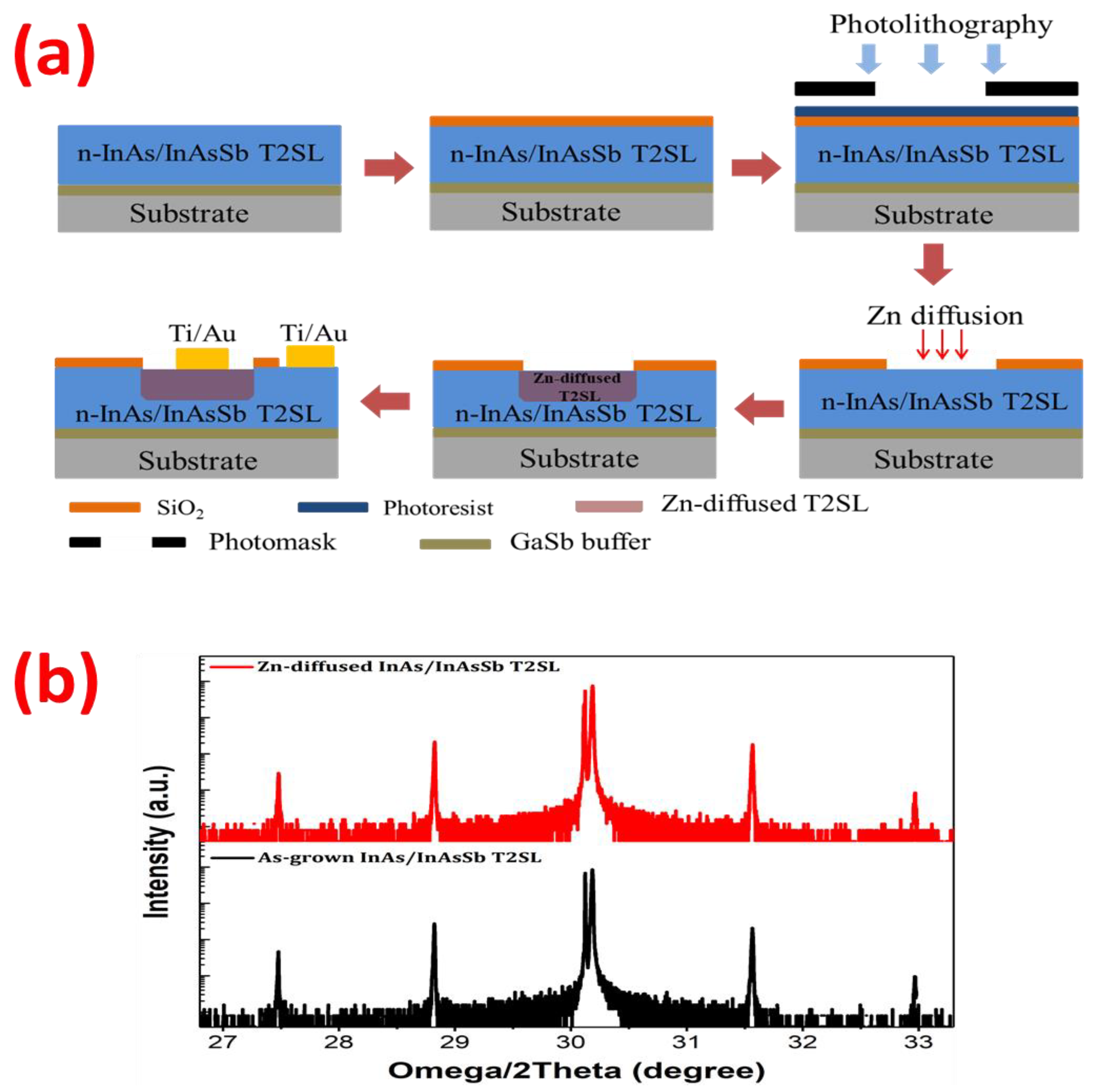
2. Materials and Methods
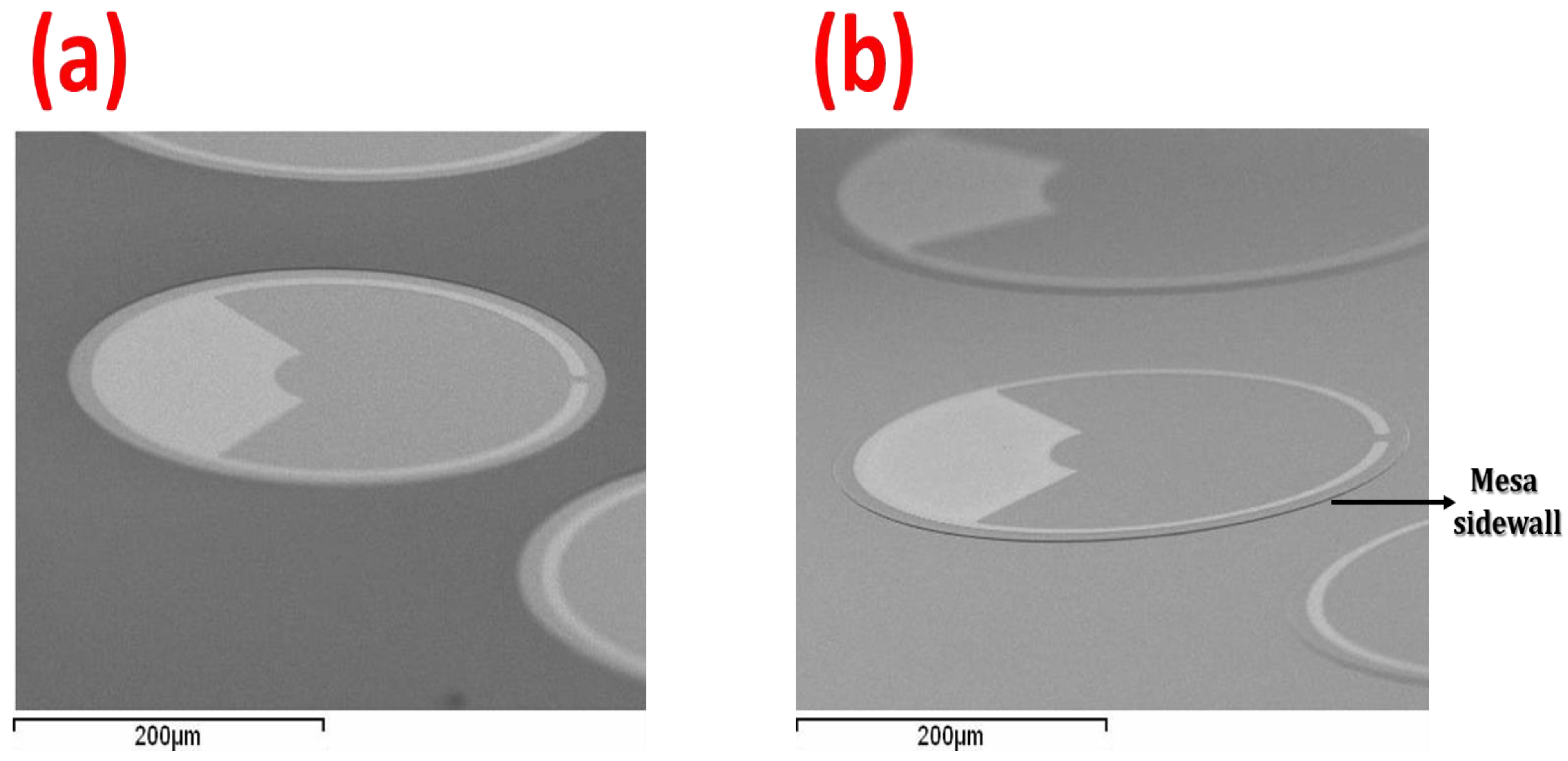
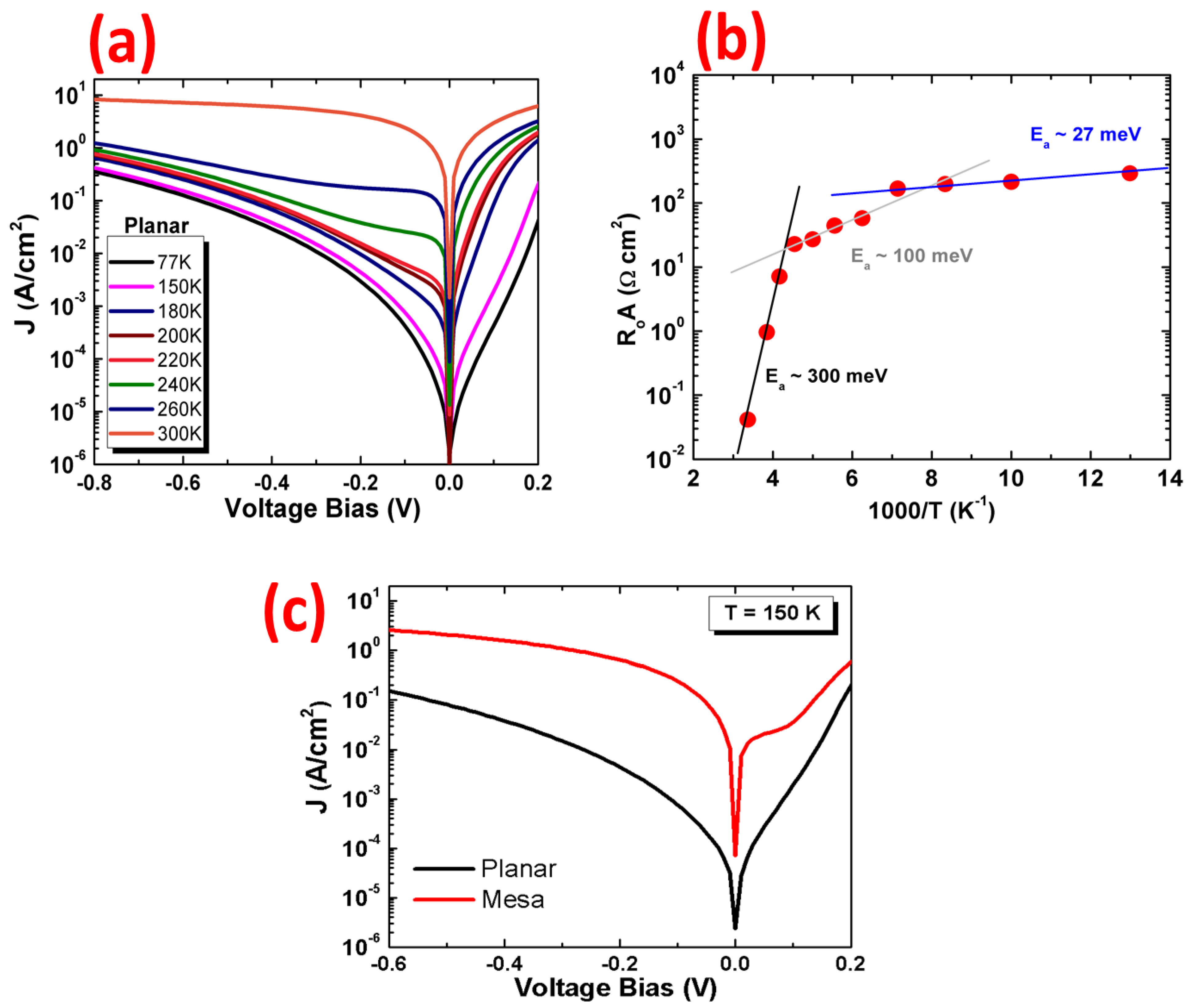
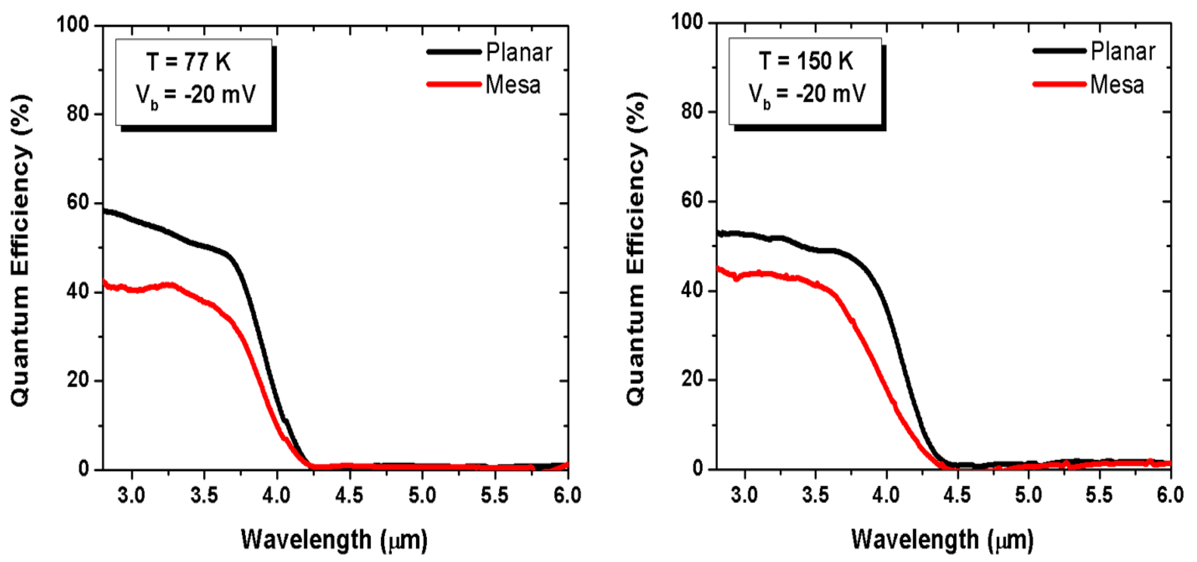
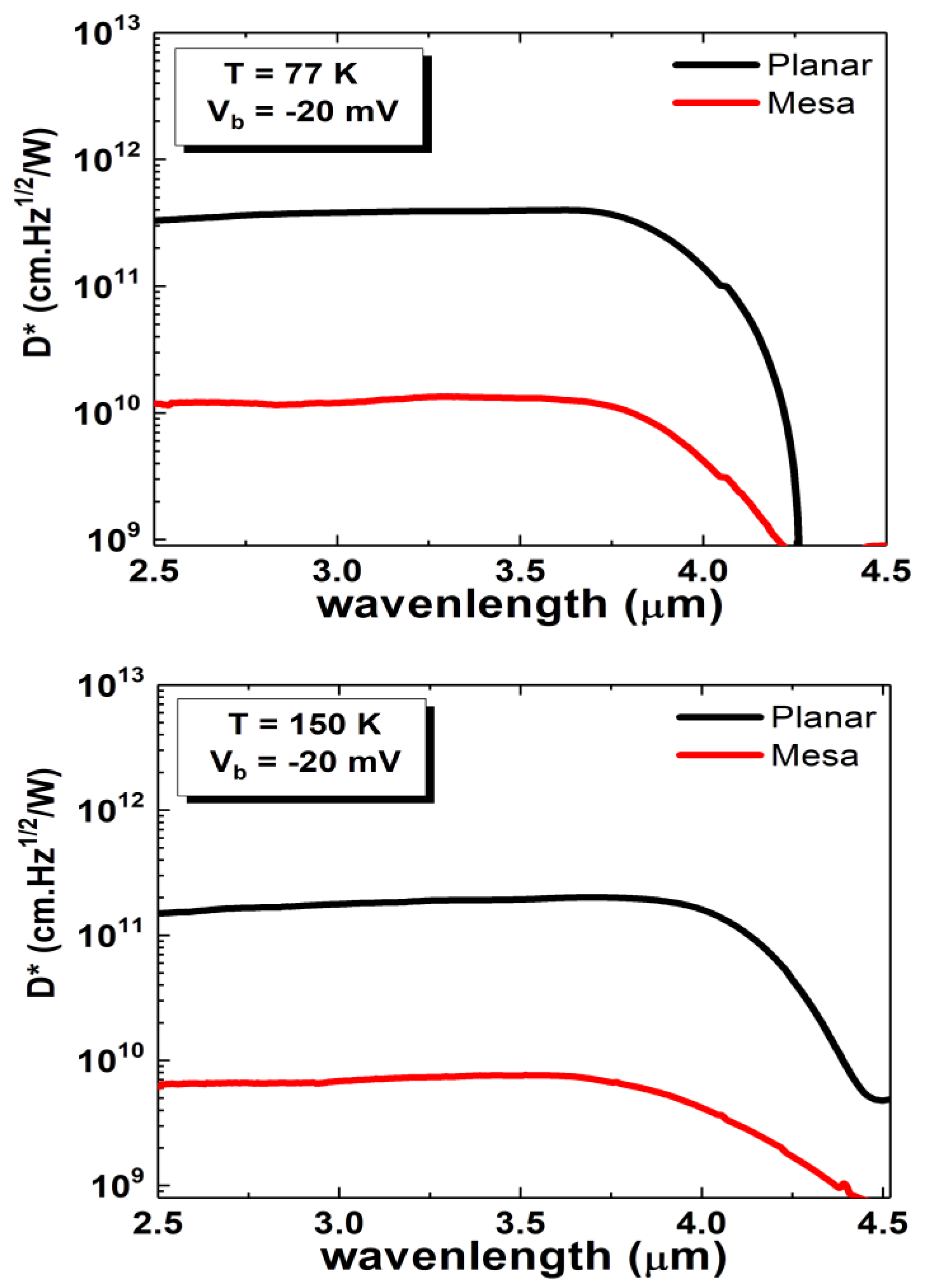
The material was grown on a 2-inch Te-doped n-type (1017 cm−3) GaSb (100) substrate at 385 °C using an Intevac Modular Gen II solid source MBE system. The growth started with a 200 nm GaSb buffer layer to stabilize the sample surface after deoxidation. Then, the active layer consisting of 2 μm unintentional doped InAs/InAs1−xSbx T2SL was grown. The superlattice design for the active layer in this work is 10/2 MLs InAs/InAs0.5Sb0.5 which has MWIR detection ability. It is also practical to form a p-n junction using Zn diffusion in InAs/InAs0.5Sb0.5 T2SL since the previous study showed that the InAs/InAsSb T2SLs are unintentionally doped n-type and the Zn is an efficient p-type dopant [33,34]. The intrinsic concentration of the as-grown unintentional doped InAs/InAsSb T2SL was evaluated to be ~5–9 × 1015 cm−3 by the Hall measurement using a InAs/InAsSb T2SL sample with the same structure grown on the GaAs substrate.
After MBE growth and material quality assessment, the sample was fabricated into the planar photodetectors. Figure 1a presents schematic diagram of the planar photodetector fabrication processes. At first, an 800 nm-thick silicon oxide (SiO2) layer was deposited on the sample surface via plasma enhanced chemical vapor deposition (PECVD) using a plasma of SiH4 and N2O gases for the diffusion mask. The diffusion window was then patterned using standard UV photolithography followed by dry etching of SiO2 layer using CF4: Ar+ plasma in an electron cyclotron resonance-reactive ion etching (ECR-RIE) system. Afterwards, the Zn diffusion process was carried out in an EMCORE metal–organic chemical vapor deposition (MOCVD) reactor at the diffusion temperature of 430 °C and the fixed reactor pressure of 60 Torr. Diethylzinc (DEZn) was used as the Zn source along with hydrogen as a carrier gas. The molar flow rate of the diethylzinc was maintained at 15 µmol/min, with a fixed diffusion time of 15 min. During the diffusion, AsH3 was used to prevent As desorption from the top T2SL layer. The sample was characterized by high resolution x-ray diffraction (HR-XRD) to investigate and compare the material quality before and after the Zn diffusion, as shown in Figure 1b. The two XRD scan curves show no main difference, indicating there was no observable material quality degradation after Zn diffusion. The satellite peaks in the HR-XRD scan show the overall periods of the active region is 37 Å, which is in good agreement with the theoretical designs. The lattice mismatch between the active layer and the GaSb substrate is ~1800 ppm. Afterwards, Ti/Au (400/1500 Å) was deposited using an electron beam evaporator for metal contacts. A standard mesa-isolated photodiode was also processed from the same wafer to have a meaningful comparison. The sample was first Zn-diffused to form a p-n junction in the MOCVD reactor at the same condition with the planar device. After that, the sample was fabricated into the mesa-isolated photodetectors via our standard mesa-isolated photodetector processing steps and the processing details can be found elsewhere [12].

3. Results

After fabrication, the T2SL planar photodetectors were characterized by the scanning electron microscope (SEM) and compared to the conventional fully etched mesa-isolated T2SL photodetectors. Figure 2a,b shows the difference of the planar device and mesa-isolated device via the SEM images. Both photodetectors are circular with diameters of 300 μm. The mesa sidewall for the fully etched mesa-isolated photodetector was marked, as shown in Figure 2b. Although the combination of dry etch and wet etch was used for mesa isolation to remove the residue and regenerate a smoother sidewall, the surface reconstruction and/or surface states exist on the mesa sidewalls due to the abrupt termination of the crystal lattice, which can lead to the surface leakage currents [35]. In the planer photodetector, no mesa sidewalls are observed since the T2SL sample was not etched which gives more stability towards any degradation as the superlattice layers are not exposed.
Both the processed planar and mesa-isolated samples were then wire-bonded onto a 68-pin leadless chip carrier (LCC) and loaded into a cryostat for electrical and optical performance characterizations. The electrical performance was first measured by the semiconductor parameter analyzer. Figure 3a shows the current-voltage (I–V) characteristics for the MWIR planar photodetector with a diameter of 320 μm at a different temperature from 77 K to 300 K. Under an applied bias voltage of −20 mV, the planar device shows a dark current density of 2.0 × 10⁻⁵ A/cm2 at 77 K and 6.4 × 10⁻⁵ A/cm2 at 150 K, corresponding to the differential-resistance-area product value of ~3.0 × 10² Ω∙cm2 at 77 K and ~60.2 Ω∙cm2 at 150 K, respectively. The Arrhenius plot of the differential resistance area product at zero bias (R0A) with respect to the inverse of temperature is shown in Figure 3b. This indicates that the dark current is dominated by different mechanisms in different temperature regimes [36]. From 77 to 140 K, the activation energy of 27 meV indicates that the device performance is limited by the temperature-insensitive defect-related leakage. From 140 to 200 K, the dominant mechanism starts to become generation recombination with an activation energy of 100 meV. Above 200 K, the planar detector is diffusion limited with an activation energy of 300 meV which is very close to the expected bandgap of the MWIR InAs/InAs1−xSbx superlattices at 200 K. As shown in Figure 3c, the dark current density of the planar photodetector at 150 K is more than two orders of magnitude lower than the mesa-isolated device, which has a dark current density of 0.024 A/cm2 under −20 mV. The improvement in dark current density for the MWIR planar device is attributed to the effective suppression of recombination mechanism at the sidewall surface, which can reduce the surface leakage currents.
Then, the planar and mesa-etched T2SL photodetectors with the diameters of 300 μm without anti-reflection (AR) coating were illuminated from the top to characterize the optical response using a calibrated 1000 °C blackbody source and a Bruker IFS 66 Fourier transform infrared (FTIR) spectrometer. The results, as shown in Figure 4, confirm the 100% cut-off wavelength of the MWIR planar photodetector at ~4.3 μm at 77 K and ~4.5 μm at 150 K, which is in agreement with the theoretical design. The quantum efficiency of both devices shows zero bias dependency at 77 K and 150 K. This indicates good material quality where the photogenerated carriers have a long diffusion length to reach the depletion region and then form the photocurrent. At 77 K, the quantum efficiency (QE) of the planar device reaches 48% at ~3.7 μm under −20 mV, corresponding to a responsivity of 1.42 A/W. The QE of planar photodetector in the MWIR range at 77 K is higher than the mesa-isolated device which has a QE of 34% at ~3.7 μm under −20 mV. At 150 K, the QE for the planar and mesa-isolated device is 49% and 37% at ~3.7 μm under −20 mV. At 150 K, the presented MWIR planar photodetector shows an improved QE and optical responsivity than the previously reported MOCVD grown Zn-diffused planar photodetector with a peak QE of 25% and responsivity value of 0.78 A/W at 3.84 μm and the ion-implanted planar photodetectors with a QE of 31.5% and peak responsivity of 0.84 A/W at 3.35 μm [31,32]. The large improvement in the optical response may be due to two reasons. First, the T2SLs grown by MBE have better material quality than the MOCVD grown materials. Second, the newly designed 10/2 InAs/InAsSb T2SL for our planar photodetector has a significantly larger absorption coefficient due to its smaller superlattice period compared with the 10/12 InAs/InAsSb T2SL used for the previously reported MOCVD grown planar photodetector [31].
To provide an overall evaluation considering both electrical and optical performance, the specific detectivity D * of the MWIR planar and the mesa-isolated photodetectors was calculated using following equation,
D * = R i ( 2 q J + 4 k b T R × A ) 1 2
where D * is the detectivity, R i is the optical responsivity, J is the dark current density, k b is the Boltzmann constant, T is the temperature and R × A is the differential resistance area product. The calculated detectivity spectrum for both samples at 77 K and 150 K is shown in Figure 5. At 77 K, the MWIR planar T2SLs-based photodetector exhibited a peak detectivity of 4.0 × 1011 cm·Hz1/2/W at the wavelength of 3.7 μm under −20 mV, which is more than one order of magnitude higher than the mesa-isolated device with the detectivity of 1.2 × 1010 cm·Hz1/2/W at 3.7 μm. At 150 K, the peak detectivity for the planar photodetector and mesa-isolated photodetector is 2.0 × 1011 cm·Hz1/2/W and 6.9 × 109 cm·Hz1/2/W, respectively, which also showed a large improvement for the planar device. The detectivity value for the planar MWIR T2SL photodetector has little change over a broad range of wavelengths from 2.5 μm to 4.0 μm at both 77 K and 150 K, indicating its potential for the imaging application. The planar device’s detectivity performance can be expected to be further improved by using proper barrier device structure design to reduce the dark current.

4. Conclusions

In summary, a mid-wavelength infrared planar photodetector based on InAs/InAs1−xSbx T2SL grown by molecular beam epitaxy has been demonstrated. The planar design for the device was achieved by Zn diffusion in a metal organic chemical vapor deposition reactor. At 77 K, the planar photodetector shows a cut-off wavelength at 4.3 μm and exhibits a peak responsivity of 1.42 A/W at 3.7 μm under −20 mV, corresponding to a quantum efficiency of 48% without anti-reflection coating. The photodetector was found to exhibit a specific detectivity of 4.0 × 1011 cm·Hz1/2/W at 3.7 μm, with a dark current density, and the differential-resistance-area product of 2.0 × 10⁻⁵ A/cm2 and ~3.0 × 10² Ω∙cm2, respectively, under a −20 mV bias at 77 K. The cut-off wavelength for the planar photodetector extends to 4.5 μm at 150 K and the peak QE reaches 49% at 3.7 μm under −20 mV bias. At 150 K, the planar photodetector shows a specific detectivity of 2.0 × 1011 cm·Hz1/2/W at 3.7 μm with a dark current density of 6.4 × 10⁻⁵ A/cm2 under an applied bias of −20 mV. The device performance of the planar photodetector showed better electrical and optical performance than the mesa-isolated photodetector at both 77 K and 150 K. In order to give better prospect and comparison, Table 1 shows the performance comparison between the planar photodetector and mesa-isolated photodetector at 150 K.

Author Contributions

Device fabrication and measurements, R.K.S., V.H.N. and J.L.; MBE growth and material characterization, J.L. and R.K.S.; MOCVD for Zn diffusion, S.S.; G.B. carried out data analysis and gave scientific input; the conceptualizing of ideas and supervision of the entire project was done by M.R.; the paper was written and revised by all the contributing authors. All authors have read and agreed to the published version of the manuscript.

Funding

This material is based upon fundamental research at CQD/Northwestern.

Data Availability Statement

The data that support the findings of this study are available from the corresponding author upon reasonable request.

Acknowledgments

The authors would like to acknowledge the interest and scientific support of Tariq Manzur for this project.

Conflicts of Interest

The authors declare no conflict of interest.

References

  1. Razeghi, M.; Dehzangi, A.; Li, J. Multi-band SWIR-MWIR-LWIR Type-II superlattice based infrared photodetector. Results Opt. 2021, 2, 100054. [Google Scholar] [CrossRef]
  2. Wartewig, S.; Neubert, R.H.H. Pharmaceutical applications of Mid-IR and Raman spectroscopy. Adv. Drug Deliv. Rev. 2005, 57, 1144–1170. [Google Scholar] [CrossRef] [PubMed]
  3. Petersen, C.R.; Møller, U.; Kubat, I.; Zhou, B.; Dupont, S.; Ramsay, J.; Benson, T.; Sujecki, S.; Abdel-Moneim, N.; Tang, Z.; et al. Mid-infrared supercontinuum covering the 1.4–13.3 μm molecular fingerprint region using ultra-high NA chalcogenide step-index fibre. Nat. Photonics 2014, 8, 830–834. [Google Scholar] [CrossRef]
  4. Kataza, H.; Wada, T.; Sakon, I.; Kobayashi, N.; Sarugaku, Y.; Fujishiro, N.; Ikeda, Y.; Oyabu, S. Mid-Infrared Camera and Spectrometer on Board SPICA; SPIE: Washington, DC, USA, 2012; Volume 8442. [Google Scholar]
  5. Marcus, C.; Andersson, K.; Åkerlind, C. Balancing the radar and long wavelength infrared signature properties in concept analysis of combat aircraft–A proof of concept. Aerosp. Sci. Technol. 2017, 71, 733–741. [Google Scholar] [CrossRef]
  6. Zheng, L.; Tidrow, M.; Aitcheson, L.; O’Connor, J.; Brown, S. Developing High-Performance III-V Superlattice IRFPAs for Defense: Challenges and Solutions; SPIE: Washington, DC, USA, 2010; Volume 7660. [Google Scholar]
  7. Zhang, L.; Pantuso, F.; Jin, G.; Mazurenko, A.; Erdtmann, M.; Radhakrishnan, S.; Salerno, J. High-Speed Uncooled MWIR Hostile Fire Indication Sensor; SPIE: Washington, DC, USA, 2011; Volume 8012. [Google Scholar]
  8. Lei, W.; Antoszewski, J.; Faraone, L. Progress, challenges, and opportunities for HgCdTe infrared materials and detectors. Appl. Phys. Rev. 2015, 2, 041303. [Google Scholar] [CrossRef]
  9. Rogalski, A.; Martyniuk, P.; Kopytko, M. Type-II superlattice photodetectors versus HgCdTe photodiodes. Prog. Quantum Electron. 2019, 68, 100228. [Google Scholar] [CrossRef]
  10. Kim, H.S.; Cellek, O.O.; Lin, Z.-Y.; He, Z.-Y.; Zhao, X.-H.; Liu, S.; Li, H.; Zhang, Y.-H. Long-wave infrared nBn photodetectors based on InAs/InAsSb type-II superlattices. Appl. Phys. Lett. 2012, 101, 161114. [Google Scholar] [CrossRef]
  11. Rogalski, A.; Martyniuk, P.; Kopytko, M. InAs/GaSb type-II superlattice infrared detectors: Future prospect. Appl. Phys. Rev. 2017, 4, 031304. [Google Scholar] [CrossRef]
  12. Li, J.; Dehzangi, A.; Brown, G.; Razeghi, M. Mid-wavelength infrared avalanche photodetector with AlAsSb/GaSb superlattice. Sci. Rep. 2021, 11, 7104. [Google Scholar] [CrossRef]
  13. Dehzangi, A.; Li, J.; Razeghi, M. Band-structure-engineered high-gain LWIR photodetector based on a type-II superlattice. Light Sci. Appl. 2021, 10, 17. [Google Scholar] [CrossRef]
  14. Li, J.; Dehzangi, A.; Wu, D.; McClintock, R.; Razeghi, M. Resonant cavity enhanced heterojunction phototransistors based on Type-II superlattices. Infrared Phys. Technol. 2020, 113, 103552. [Google Scholar] [CrossRef]
  15. Salihoglu, O.; Muti, A.; Kutluer, K.; Tansel, T.; Turan, R.; Kocabas, C.; Aydinli, A. Passivation of Type II InAs/GaSb Superlattice Photodetectors with Atomic Layer Deposited Al2O3; SPIE: Washington, DC, USA, 2012; Volume 8353. [Google Scholar]
  16. Kim, H.S. Passivation Study of InAs/GaSb Type-II Strained Layer Superlattice in Mid-wave Infrared Photodetector. J. Korean Phys. Soc. 2020, 77, 714–718. [Google Scholar] [CrossRef]
  17. Ren, D.; Azizur-Rahman, K.M.; Rong, Z.; Juang, B.-C.; Somasundaram, S.; Shahili, M.; Farrell, A.C.; Williams, B.S.; Huffaker, D.L. Room-Temperature Midwavelength Infrared InAsSb Nanowire Photodetector Arrays with Al2O3 Passivation. Nano Lett. 2019, 19, 2793–2802. [Google Scholar] [CrossRef] [PubMed]
  18. Zhang, S.; Jiao, H.; Wang, X.; Chen, Y.; Wang, H.; Zhu, L.; Jiang, W.; Liu, J.; Sun, L.; Lin, T.; et al. Highly Sensitive InSb Nanosheets Infrared Photodetector Passivated by Ferroelectric Polymer. Adv. Funct. Mater. 2020, 30, 2006156. [Google Scholar] [CrossRef]
  19. Kinch, M. The Rationale for Ultra-Small Pitch IR Systems; SPIE: Washington, DC, USA, 2014; Volume 9070. [Google Scholar]
  20. Rogalski, A.; Martyniuk, P.; Kopytko, M. Challenges of small-pixel infrared detectors: A review. Rep. Prog. Phys. 2016, 79, 046501. [Google Scholar] [CrossRef]
  21. Rutkowski, J. Planar junction formation in HgCdTe infrared detectors. Opto-Electron. Rev. 2004, 12, 123–128. [Google Scholar]
  22. Musca, C.A.; Antoszewski, J.; Dell, J.M.; Faraone, L.; Terterian, S. Planar p-on-n HgCdTe heterojunction mid-wavelength infrared photodiodes formed using plasma-induced junction isolation. J. Electron. Mater. 2003, 32, 622–626. [Google Scholar] [CrossRef]
  23. Iwamura, Y.; Watanabe, N. InAs Planar Diode Fabricated by Zn Diffusion. Jpn. J. Appl. Phys. 2000, 39, 5740–5745. [Google Scholar] [CrossRef]
  24. Pitts, O.J.; Hisko, M.; Benyon, W.; Raymond, S.; SpringThorpe, A.J. Optimization of MOCVD-diffused p-InP for planar avalanche photodiodes. J. Cryst. Growth 2014, 393, 85–88. [Google Scholar] [CrossRef]
  25. Wang, T.; Xiong, M.; Zhao, Y.; Dong, X.; Zhao, Y.; Miao, J.; Huang, Y.; Zhang, B.; Cao, L.; Dong, B. Planar mid-infrared InAsSb photodetector grown on GaAs substrates by MOCVD. Appl. Phys. Express 2019, 12, 122009. [Google Scholar] [CrossRef]
  26. Saroj, R.K.; Nguyen, V.H.; Slivken, S.; Brown, G.J.; Razeghi, M. Demonstration of Zn-diffused planar long-wavelength infrared photodetector based on type-II superlattice grown by MBE. IEEE J. Quantum Elect. 2022, 58, 4000306. [Google Scholar] [CrossRef]
  27. Hurwitz, C.E.; Donnelly, J.P. Planar InSb photodiodes fabricated by Be and Mg ion implantation. Solid-State Electron. 1975, 18, 753–756. [Google Scholar] [CrossRef]
  28. Lee, K.-C.; Lin, M.-X.; Li, H.; Cheng, H.-H.; Sun, G.; Soref, R.; Hendrickson, J.R.; Hung, K.-M.; Scajev, P.; Medvids, A. Planar GeSn photodiode for high-detectivity photodetection at 1550 nm. Appl. Phys. Lett. 2020, 117, 012102. [Google Scholar] [CrossRef]
  29. Ettenberg, M.; Dianat, P.; Lange, M.; Sudol, T.; Nguyen, H.; Gil, A.; Ahmed, N.; Phillips, J. Extended-Wavelength 1.3-Megapixel Type-II Superlattice SWIR Compact Camera System with Scalable Manufacturing; SPIE: Washington, DC, USA, 2022; Volume 11997. [Google Scholar]
  30. Rajavel, R.; Nosho, B.; Terterian, S.; Bui, S.; Royter, Y.; de Lyon, T. Fabrication of InAs/GaSb Type-II Superlattice LWIR Planar Photodiodes; SPIE: Washington, DC, USA, 2009; Volume 7298. [Google Scholar]
  31. Wu, D.; Dehzangi, A.; Li, J.; Razeghi, M. High performance Zn-diffused planar mid-wavelength infrared type-II InAs/InAs1−xSbx superlattice photodetector by MOCVD. Appl. Phys. Lett. 2020, 116, 161108. [Google Scholar] [CrossRef]
  32. Dehzangi, A.; Wu, D.; McClintock, R.; Li, J.; Razeghi, M. Planar nBn type-II superlattice mid-wavelength infrared photodetectors using zinc ion-implantation. Appl. Phys. Lett. 2020, 116, 221103. [Google Scholar] [CrossRef]
  33. Steenbergen, E.H.; Connelly, B.C.; Metcalfe, G.D.; Shen, H.; Wraback, M.; Lubyshev, D.; Qiu, Y.; Fastenau, J.M.; Liu, A.W.K.; Elhamri, S.; et al. Significantly improved minority carrier lifetime observed in a long-wavelength infrared III-V type-II superlattice comprised of InAs/InAsSb. Appl. Phys. Lett. 2011, 99, 251110. [Google Scholar] [CrossRef]
  34. Lackner, D.; Pitts, O.J.; Steger, M.; Yang, A.; Thewalt, M.L.W.; Watkins, S.P. Strain balanced InAs/InAsSb superlattice structures with optical emission to 10 μm. Appl. Phys. Lett. 2009, 95, 081906. [Google Scholar] [CrossRef]
  35. Zhang, Z.; Yates, J.T. Band Bending in Semiconductors: Chemical and Physical Consequences at Surfaces and Interfaces. Chem. Rev. 2012, 112, 5520–5551. [Google Scholar] [CrossRef]
  36. Lanir, M.; Riley, K.J. Performance of PV HgCdTe arrays for 1-14-µm applications. IEEE Trans. Electron. Devices 1982, 29, 274–279. [Google Scholar] [CrossRef]
Figure 1. (a) Schematic diagram of fabrication processes for the Zn-diffused planar photodetector based on InAs/InAsSb T2SL. (b) HR-XRD scan curve of the as-grown (black) and Zn-diffused (red) InAs/InAsSb T2SL on GaSb substrate.
Photonics 09 00664 g001
Figure 2. (a) Scanning electron microscope (SEM) image of the planar photodetectors. (b) SEM image of the conventional fully etched mesa-isolated T2SL photodetector where the mesa sidewall was marked.
Photonics 09 00664 g002
Figure 3. (a) Dark current density vs. applied bias voltage characteristics for the MWIR planar photodetector at different temperatures. (b) R0A vs. 1/T relation from 77 K to 300 K (c) Comparison of the dark current density of the planar and mesa-etched photodetectors at 150 K.
Photonics 09 00664 g003
Figure 4. The comparison between the quantum efficiency spectra of the T2SL planar photodetector and mesa-isolated photodetector under −20 mV at 77 K (left) and 150 K (right).
Photonics 09 00664 g004
Figure 5. The comparison between the specific detectivity ( D * ) spectral for the MWIR planar photodetector and mesa-isolated photodetector under −20 mV at 77 K (up) and 150 K (down).
Photonics 09 00664 g005
Table 1. Performance comparison between the planar MWIR photodetector and mesa-isolated photodetector at 150 K.
DeviceDark Current Density (A/cm2)QESpecific Detectivity (cm·Hz1/2/W)
PLANAR6.4 × 10−549%2.0 × 10¹¹
MESA2.4 × 10−237%6.9 × 10⁹
Publisher’s Note: MDPI stays neutral with regard to jurisdictional claims in published maps and institutional affiliations.

